 | ÐлекÑÑоннÑй компоненÑ: BGY585A | СкаÑаÑÑ:  PDF PDF  ZIP ZIP |
Äîêóìåíòàöèÿ è îïèñàíèÿ www.docs.chipfind.ru
DATA SHEET
Product specification
Supersedes data of 1997 Apr 14
1999 Mar 26
DISCRETE SEMICONDUCTORS
BGY585A
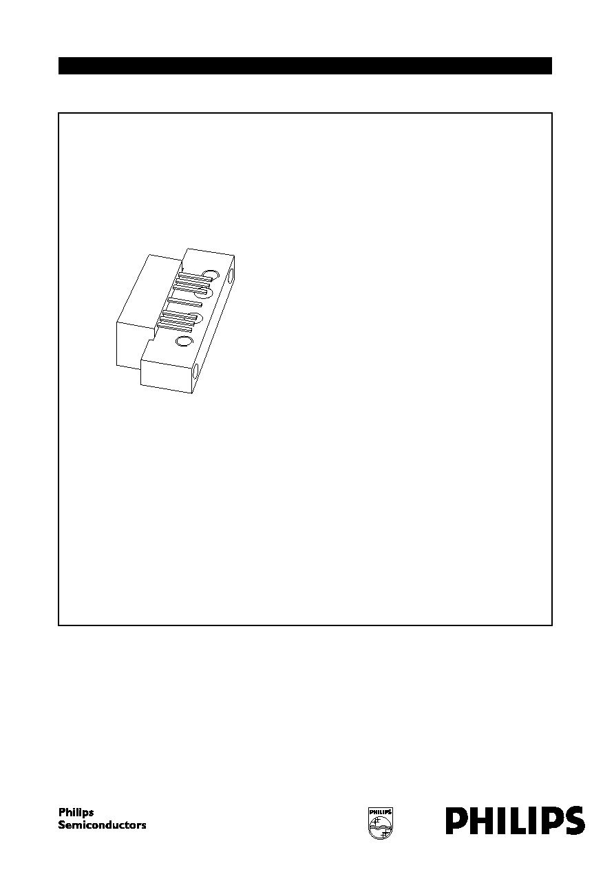
CATV amplifier module
book, halfpage
M3D252
1999 Mar 26
2
Philips Semiconductors
Product specification
CATV amplifier module
BGY585A
FEATURES
·
Excellent linearity
·
Extremely low noise
·
Silicon nitride passivation
·
Rugged construction
·
Optimal reliability ensured by
TiPtAu metallized crystals.
DESCRIPTION
Hybrid amplifier module for CATV
systems operating over a frequency
range of 40 to 550 MHz at a voltage
supply of 24 V (DC). Intended for use
as a final amplifier.
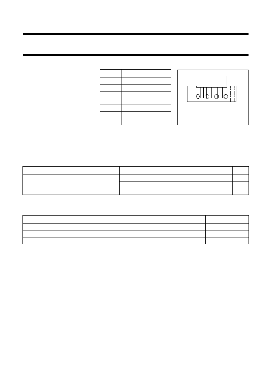
PINNING - SOT115J
PIN
DESCRIPTION
1
input
2
common
3
common
5
+V
B
7
common
8
common
9
output
PIN CONFIGURATION
Fig.1 Simplified outline.
fpage
7
8
9
2
3
5
1
Side view
MSA319
QUICK REFERENCE DATA
LIMITING VALUES
In accordance with the Absolute Maximum Rating System (IEC 134).
SYMBOL
PARAMETER
CONDITIONS
MIN.
TYP.
MAX.
UNIT
G
p
power gain
f = 50 MHz
17.7
-
18.7
dB
f = 550 MHz
18.8
-
20
dB
I
tot
total current consumption (DC)
V
B
= 24 V
-
220
240
mA
SYMBOL
PARAMETER
MIN.
MAX.
UNIT
V
i
RF input voltage
-
65
dBmV
T
stg
storage temperature
-
40
+100
°
C
T
case
case operating temperature
-
20
+100
°
C
1999 Mar 26
3
Philips Semiconductors
Product specification
CATV amplifier module
BGY585A
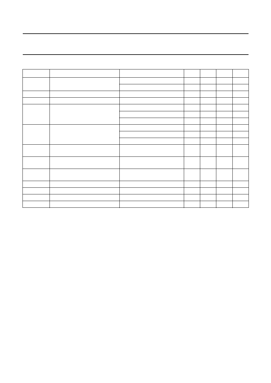
CHARACTERISTICS
Table 1
Bandwidth 40 to 550 MHz; T
case
= 30
°
C; Z
S
= Z
L
= 75
Notes
1. f
p
= 55.25 MHz; V
p
= 44 dBmV;
f
q
= 493.25 MHz; V
q
= 44 dBmV;
measured at f
p
+ f
q
= 548.5 MHz.
2. Measured according to DIN45004B;
f
p
= 540.25 MHz; V
p
= V
o
;
f
q
= 547.25 MHz; V
q
= V
o
-
6 dB;
f
r
= 549.25 MHz; V
r
= V
o
-
6 dB;
measured at f
p
+ f
q
-
f
r
= 538.25 MHz.
3. The module normally operates at V
B
= 24 V, but is able to withstand supply transients up to 30 V.
SYMBOL
PARAMETER
CONDITIONS
MIN.
TYP.
MAX.
UNIT
G
p
power gain
f = 50 MHz
17.7
-
18.7
dB
f = 550 MHz
18.8
-
20
dB
SL
slope cable equivalent
f = 40 to 550 MHz
0.5
-
2
dB
FL
flatness of frequency response
f = 40 to 550 MHz
-
-
±
0.2
dB
S
11
input return losses
f = 40 to 80 MHz
20
-
-
dB
f = 80 to 160 MHz
19
-
-
dB
f = 160 to 550 MHz
18
-
-
dB
S
22
output return losses
f = 40 to 80 MHz
20
-
-
dB
f = 80 to 160 MHz
19
-
-
dB
f = 160 to 550 MHz
18
-
-
dB
CTB
composite triple beat
77 channels flat; V
o
= 44 dBmV;
measured at 547.25 MHz
-
-
-
59
dB
X
mod
cross modulation
77 channels flat; V
o
= 44 dBmV;
measured at 55.25 MHz
-
-
-
62
dB
CSO
composite second order distortion
77 channels flat; V
o
= 44 dBmV;
measured at 548.5 MHz
-
-
-
59
dB
d
2
second order distortion
note 1
-
-
-
72
dB
V
o
output voltage
d
im
=
-
60 dB; note 2
61.5
-
-
dBmV
F
noise figure
f = 550 MHz
-
-
8
dB
I
tot
total current consumption (DC)
V
B
= 24 V; note 3
-
220
240
mA
1999 Mar 26
4
Philips Semiconductors
Product specification
CATV amplifier module
BGY585A
Table 2
Bandwidth 40 to 450 MHz; T
case
= 30
°
C; Z
S
= Z
L
= 75
Notes
1. f
p
= 55.25 MHz; V
p
= 46 dBmV;
f
q
= 391.25 MHz; V
q
= 46 dBmV;
measured at f
p
+ f
q
= 446.5 MHz.
2. Measured according to DIN45004B;
f
p
= 440.25 MHz; V
p
= V
o
;
f
q
= 447.25 MHz; V
q
= V
o
-
6 dB;
f
r
= 449.25 MHz; V
r
= V
o
-
6 dB; measured at f
p
+ f
q
-
f
r
= 438.25 MHz.
3. The module normally operates at V
B
= 24 V, but is able to withstand supply transients up to 30 V.
SYMBOL
PARAMETER
CONDITIONS
MIN.
TYP.
MAX.
UNIT
G
p
power gain
f = 50 MHz
17.7
-
18.7
dB
f = 450 MHz
18.6
-
19.8
dB
SL
slope cable equivalent
f = 40 to 450 MHz
0.5
-
1.8
dB
FL
flatness of frequency response
f = 40 to 450 MHz
-
-
±
0.2
dB
S
11
input return losses
f = 40 to 80 MHz
20
-
-
dB
f = 80 to 160 MHz
19
-
-
dB
f = 160 to 450 MHz
18
-
-
dB
S
22
output return losses
f = 40 to 80 MHz
20
-
-
dB
f = 80 to 160 MHz
19
-
-
dB
f = 160 to 450 MHz
18
-
-
dB
CTB
composite triple beat
60 channels flat; V
o
= 46 dBmV;
measured at 445.25 MHz
-
-
-
61
dB
X
mod
cross modulation
60 channels flat; V
o
= 46 dBmV;
measured at 55.25 MHz
-
-
-
61
dB
CSO
composite second order distortion
60 channels flat; V
o
= 46 dBmV;
measured at 446.5 MHz
-
-
-
61
dB
d
2
second order distortion
note 1
-
-
-
75
dB
V
o
output voltage
d
im
=
-
60 dB; note 2
64
-
-
dBmV
F
noise figure
f = 450 MHz
-
-
7
dB
I
tot
total current consumption (DC)
V
B
= 24 V; note 3
-
220
240
mA
1999 Mar 26
5
Philips Semiconductors
Product specification
CATV amplifier module
BGY585A
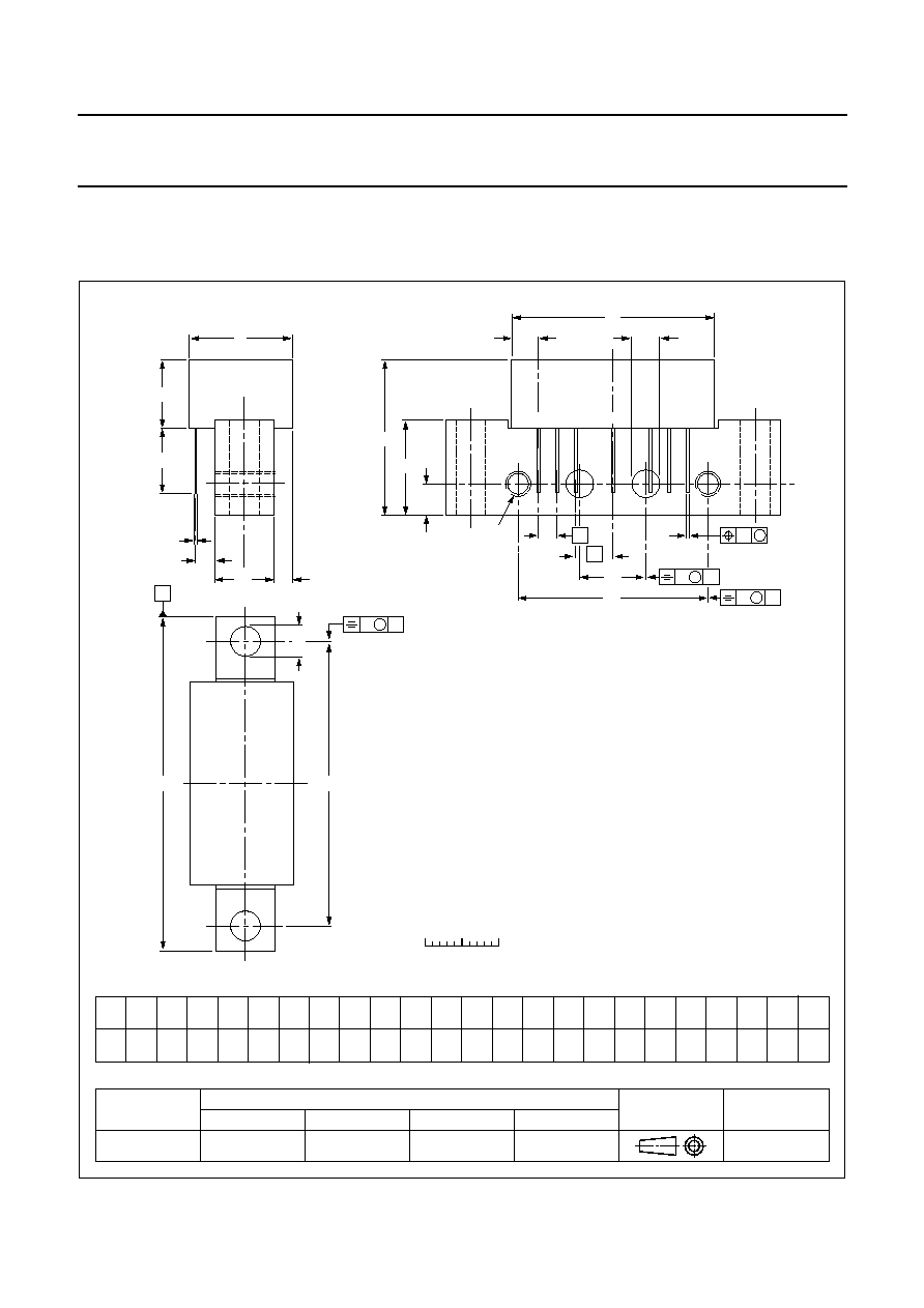
PACKAGE OUTLINE
UNIT
A2
max.
c
e
e1
q
Q
max.
q1
q2
U1
max.
U2
W
REFERENCES
OUTLINE
VERSION
EUROPEAN
PROJECTION
ISSUE DATE
IEC
JEDEC
EIAJ
mm
20.8
9.1
0.51
0.38
0.25 27.2 2.54 13.75 2.54 5.08 12.7
8.8
4.15
3.85
2.4
38.1 25.4 10.2
4.2 44.75
8
0.25
0.1
3.8
b
F
p
6-32
UNC
y
w
S
DIMENSIONS (mm are the original dimensions)
SOT115J
0
5
10 mm
scale
A
max.
D
max.
L
min.
E
max.
Z
max.
Rectangular single-ended package; aluminium flange; 2 vertical mounting holes;
2 x 6-32 UNC and 2 extra horizontal mounting holes; 7 gold-plated in-line leads
SOT115J
D
U1
q
q2
q1
b
F
S
A
Z
p
E
A2
L
c
d
Q
U2
M
w
7
8
9
2
3
W
e
e1
5
p
1
d
max.
y
M
B
y
M
B
B
99-02-06
y
M
B