 | ÐлекÑÑоннÑй компоненÑ: BLF276 | СкаÑаÑÑ:  PDF PDF  ZIP ZIP |
Äîêóìåíòàöèÿ è îïèñàíèÿ www.docs.chipfind.ru
DATA SHEET
Product specification
December 1997
DISCRETE SEMICONDUCTORS
BLF276
VHF power MOS transistor
December 1997
2
Philips Semiconductors
Product specification
VHF power MOS transistor
BLF276
FEATURES
·
High power gain
·
Easy power control
·
Good thermal stability
DESCRIPTION
Silicon N-channel enhancement
mode vertical D-MOS transistor
designed for large signal amplifier
applications in the VHF frequency
range. The transistor delivers an
output power of 100 W in class-B
operation at a supply voltage of 50 V.
The transistor is encapsulated in a
6-lead, SOT119 pill-package
envelope, with a ceramic cap.
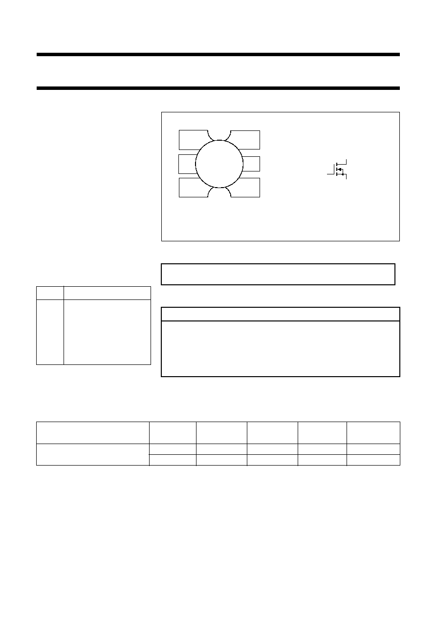
PINNING - SOT119D3
PIN
DESCRIPTION
1
source
2
source
3
gate
4
drain
5
source
6
source
PIN CONFIGURATION
CAUTION
The device is supplied in an antistatic package. The gate-source input must
be protected against static charge during transport and handling.
WARNING
Product and environmental safety - toxic materials
This product contains beryllium oxide. The product is entirely safe provided
that the BeO disc is not damaged. All persons who handle, use or dispose of
this product should be aware of its nature and of the necessary safety
precautions. After use, dispose of as chemical or special waste according to
the regulations applying at the location of the user. It must never be thrown
out with the general or domestic waste.
Fig.1 Simplified outline and symbol.
page
2
4
6
5
3
1
MSA308
Top view
s
d
g
MBB072
QUICK REFERENCE DATA
RF performance at T
mb
= 25
°
C in a common source test circuit.
MODE OF OPERATION
f
(MHz)
V
DS
(V)
P
L
(W)
G
P
(dB)
D
(%)
CW, class-B
225
50
100
13
50
108
50
100
18
60
December 1997
3
Philips Semiconductors
Product specification
VHF power MOS transistor
BLF276
LIMITING VALUES
In accordance with the Absolute Maximum System (IEC 134).
THERMAL RESISTANCE
SYMBOL
PARAMETER
CONDITIONS
MIN.
MAX.
UNIT
V
DS
drain-source voltage
-
110
V
±
V
GS
gate-source voltage
-
20
V
I
D
DC drain current
-
9
A
P
tot
total power dissipation
up to T
mb
= 25
°
C
-
150
W
T
stg
storage temperature
-
65
150
°
C
T
j
junction temperature
-
200
°
C
SYMBOL
PARAMETER
CONDITIONS
THERMAL RESISTANCE
R
th j-mb
thermal resistance from junction to
mounting base
P
tot
= 150 W; T
mb
= 25
°
C
max. 1.17 K/W
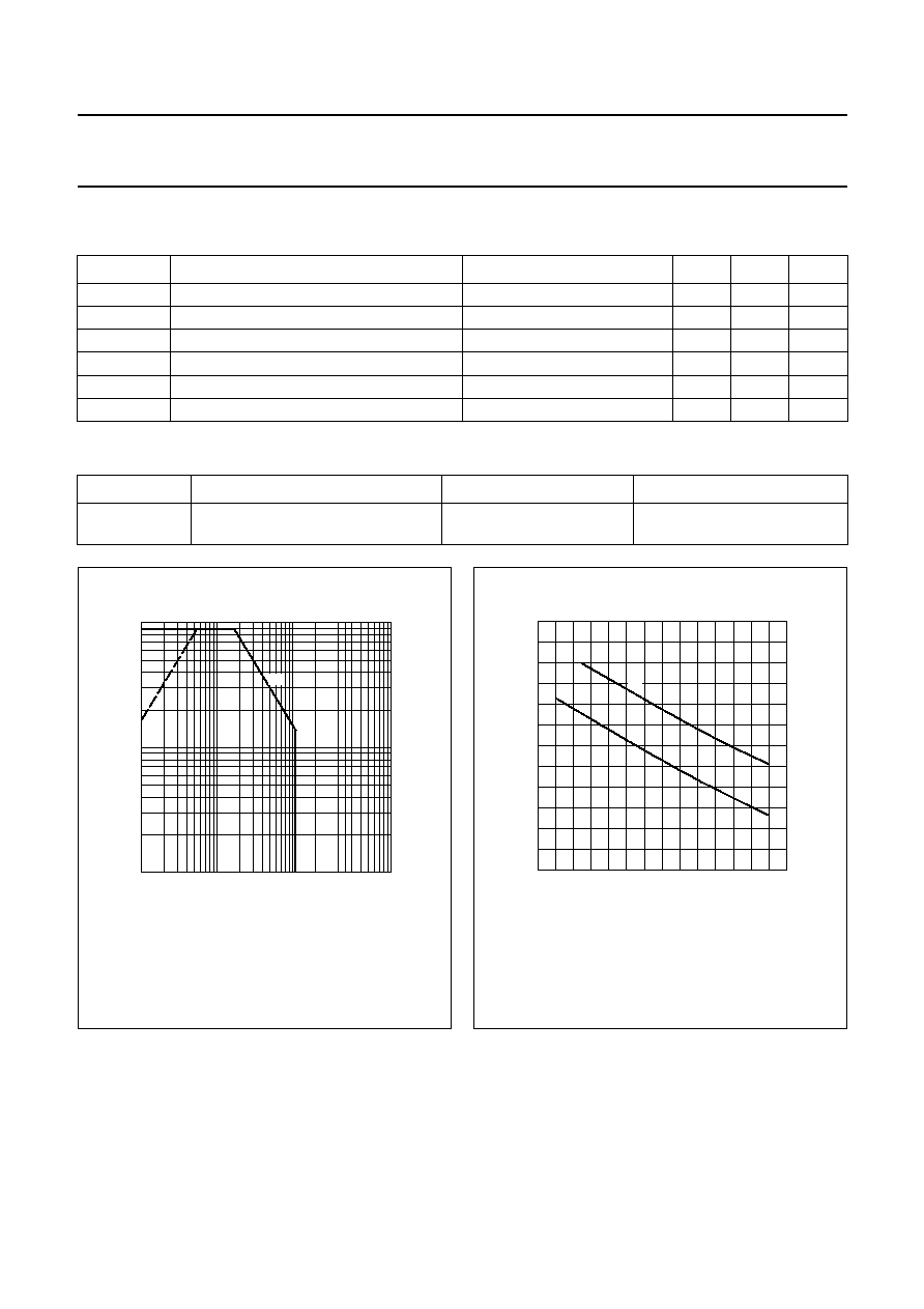
Fig.2 DC SOAR.
(1) Current is this area may be limited by R
DS(on)
.
(2) T
mb
= 25
°
C.
handbook, halfpage
10
-
1
1
ID
(A)
10
1
10
VDS (V)
10
2
10
3
(1)
MRA936
(2)
Fig.3 Power/temperature derating curves.
(1) Continuous operation.
(2) Short-time operation during mismatch.
handbook, halfpage
0
40
80
120
160
200
240
0
20
Ptot
(W)
40
60
80
100
Tmb (
°
C)
120
140
(1)
(2)
MRA943
December 1997
4
Philips Semiconductors
Product specification
VHF power MOS transistor
BLF276
CHARACTERISTICS
T
j
= 25
°
C unless otherwise specified.
SYMBOL
PARAMETER
CONDITIONS
MIN.
TYP.
MAX. UNIT
V
(BR)DSS
drain-source breakdown voltage
V
GS
= 0; I
D
= 30 mA
110
-
-
V
I
DSS
drain-source leakage current
V
GS
= 0; V
DS
= 50 V
-
-
1
mA
I
GSS
gate-source leakage current
±
V
GS
= 20 V; V
DS
= 0
-
-
1
µ
A
V
GS(th)
gate-source threshold voltage
I
D
= 50 mA; V
DS
= 10 V
2
-
4.5
V
g
fs
forward transconductance
I
D
= 3 A; V
DS
= 10 V
2.7
-
-
S
R
DS(on)
drain-source on-state resistance
I
D
= 3 A; V
GS
= 10 V
-
0.4
0.6
I
DSX
on-state drain current
V
GS
= 10 V; V
DS
= 10 V
8
12
-
A
C
is
input capacitance
V
GS
= 0; V
DS
= 50 V; f = 1 MHz
-
240
-
pF
C
os
output capacitance
V
GS
= 0; V
DS
= 50 V; f = 1 MHz
-
95
-
pF
C
rs
feedback capacitance
V
GS
= 0; V
DS
= 50 V; f = 1 MHz
-
7
-
pF
Fig.4
Temperature coefficient of gate-source
voltage as a function of drain current, typical
values.
V
DS
= 10 V.
handbook, halfpage
0
-
1
-
2
-
3
-
4
-
5
10
-
1
10
10
-
2
1
ID (A)
TC
(mV/K)
MRA945
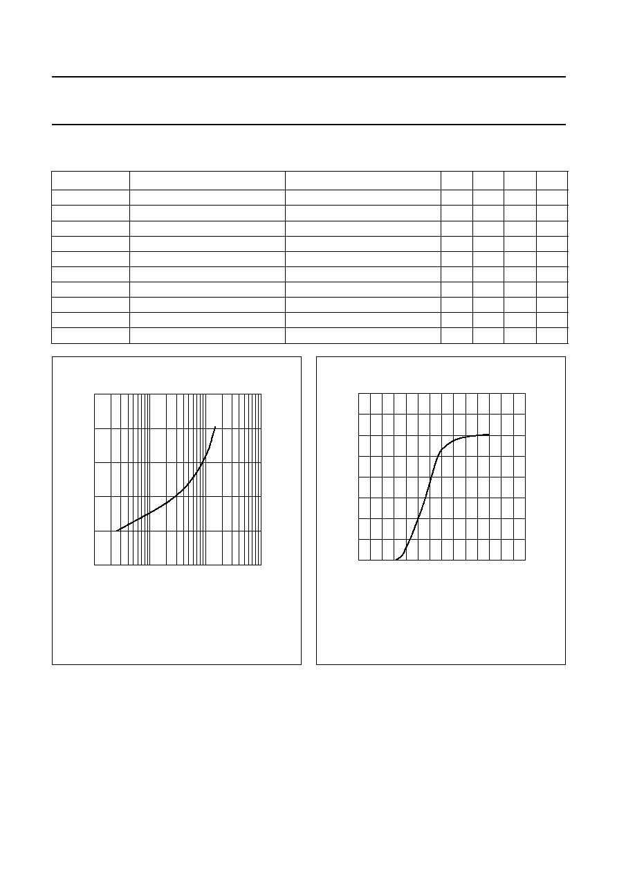
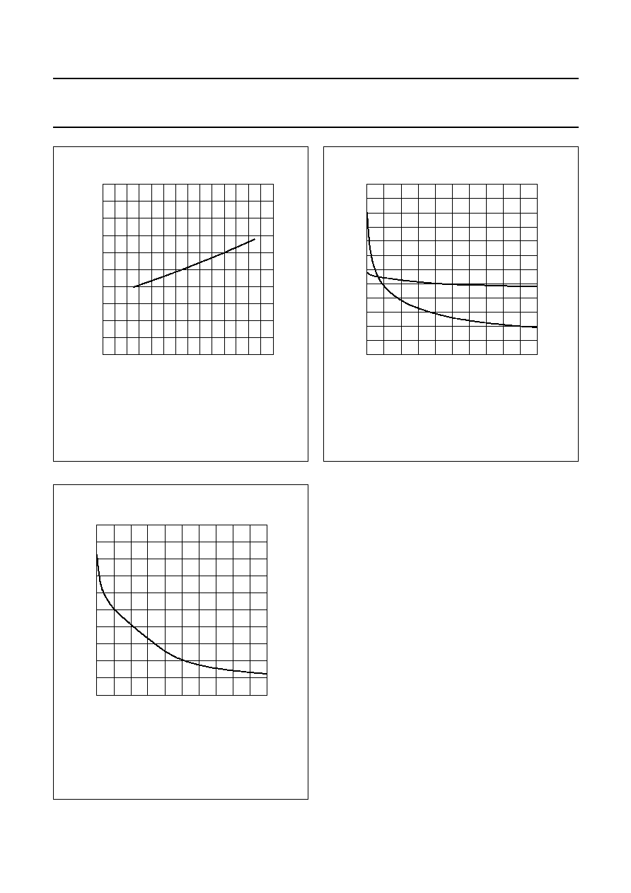
Fig.5
Drain current as a function of gate-source
voltage, typical values.
V
DS
= 10 V.
handbook, halfpage
0
4
8
12
16
0
2
4
6
8
ID
(A)
10
VGS (V)
12
14
MRA940
December 1997
5
Philips Semiconductors
Product specification
VHF power MOS transistor
BLF276
Fig.6
Drain-source on-state resistance as a
function of junction temperature, typical
values.
I
D
= 3 A; V
GS
= 10 V.
handbook, halfpage
0
0.2
0.4
0.6
0.8
1
0
20
40
RDS (on)
(
)
60
80
100
Tj (
°
C)
120
140
MRA944
Fig.7
Input and output capacitance as functions
of drain-source voltage, typical values.
V
GS
= 0; f = 1 MHz.
handbook, halfpage
0
100
200
300
400
500
600
0
10
20
C
(pF)
30
VDS (V)
Cis
Cos
40
50
MRA934
Fig.8
Feedback capacitance as a function of
drain-source voltage, typical values.
V
GS
= 0; f = 1 MHz.
handbook, halfpage
0
10
20
30
40
50
0
10
Crs
(pF)
20
30
VDS (V)
40
50
MRA935
Document Outline
- FEATURES
- DESCRIPTION
- PINNING - SOT119D3
- PIN CONFIGURATION
- QUICK REFERENCE DATA
- LIMITING VALUES
- THERMAL RESISTANCE
- CHARACTERISTICS
- APPLICATION INFORMATION FOR CLASS-B OPERATION
- Ruggedness in class-B operation
- List of components (class-B test circuit)
- PACKAGE OUTLINE
- DEFINITIONS
- LIFE SUPPORT APPLICATIONS