 | ÐлекÑÑоннÑй компоненÑ: BLV99 | СкаÑаÑÑ:  PDF PDF  ZIP ZIP |
Äîêóìåíòàöèÿ è îïèñàíèÿ www.docs.chipfind.ru
DATA SHEET
Product specification
September 1991
DISCRETE SEMICONDUCTORS
BLV99/SL
UHF power transistor
September 1991
2
Philips Semiconductors
Product specification
UHF power transistor
BLV99/SL
FEATURES
·
Emitter-ballasting resistors for an
optimum temperature profile
·
Gold metallization ensures
excellent reliability.
DESCRIPTION
NPN silicon planar epitaxial transistor
encapsulated in a 4-lead SOT172D
envelope with a ceramic cap. It is
designed primarily for use as a driver
stage in base stations in the 900 MHz
communications band. All leads are
isolated from the mounting base.
PINNING - SOT172D
PIN
DESCRIPTION
1
emitter
2
base
3
collector
4
emitter
PIN CONFIGURATION
QUICK REFERENCE DATA
RF performance at T
mb
= 25
°
C in a common emitter class-B test circuit.
WARNING
Product and environmental safety - toxic materials
This product contains beryllium oxide. The product is entirely safe provided
that the BeO disc is not damaged. All persons who handle, use or dispose of
this product should be aware of its nature and of the necessary safety
precautions. After use, dispose of as chemical or special waste according to
the regulations applying at the location of the user. It must never be thrown
out with the general or domestic waste.
MODE OF
OPERATION
f
(MHz)
V
CE
(V)
P
L
(W)
G
p
(dB)
c
(%)
c.w. narrow band
900
24
2
>
8
>
55
handbook, halfpage
e
c
b
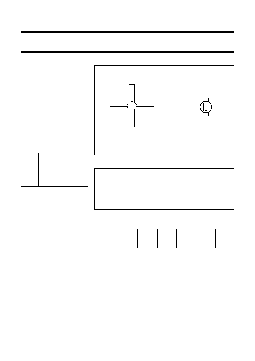
MBB012
Fig.1 Simplified outline and symbol.
halfpage
2
1
4
3
MSB007
Top view
September 1991
3
Philips Semiconductors
Product specification
UHF power transistor
BLV99/SL
LIMITING VALUES
In accordance with the Absolute Maximum System (IEC 134).
THERMAL RESISTANCE
SYMBOL
PARAMETER
CONDITIONS
MIN.
MAX.
UNIT
V
CBO
collector-base voltage
open emitter
-
50
V
V
CEO
collector-emitter voltage
open base
-
27
V
V
EBO
emitter-base voltage
open collector
-
3.5
V
I
C
collector current
DC value
-
200
mA
I
CM
collector current
peak value
f
>
1 MHz
-
600
mA
P
tot
total power dissipation
f
>
1 MHz;
T
mb
= 50
°
C
-
6
W
T
stg
storage temperature range
-
65
150
°
C
T
j
junction operating temperature
-
200
°
C
SYMBOL
PARAMETER
CONDITIONS
MAX.
UNIT
R
th j-mb(RF)
from junction to mounting base
P
L
= 4.5 W; T
mb
= 25
°
C
20
K/W
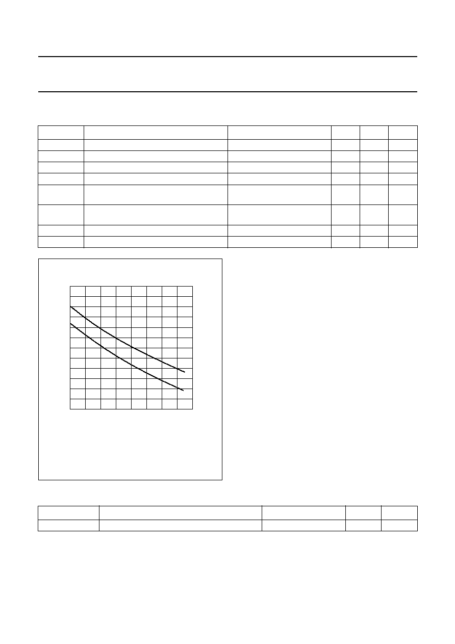
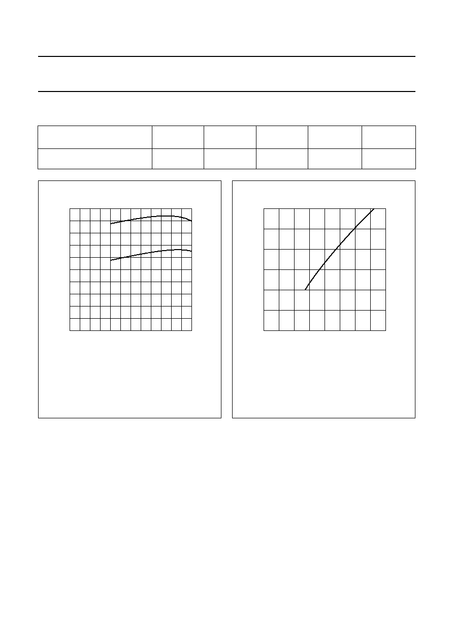
Fig.2 Power/temperature derating curves.
(I) Continuous RF operation.
(II) Short time operation during mismatch.
handbook, halfpage
0
40
80
160
Th (
°
C)
Ptot
(W)
12
0
4
8
120
MBK466
September 1991
4
Philips Semiconductors
Product specification
UHF power transistor
BLV99/SL
CHARACTERISTICS
T
j
= 25
°
C.
SYMBOL
PARAMETER
CONDITIONS
MIN.
TYP.
MAX.
UNIT
V
(BR)CBO
collector-base breakdown voltage
open emitter;
I
C
= 5 mA
50
-
-
V
V
(BR)CEO
collector-emitter breakdown voltage
V
BE
= 0;
I
C
= 10 mA
27
-
-
V
V
(BR)EBO
emitter-base breakdown voltage
open collector;
I
E
= 0.5 mA
3.5
-
-
V
I
CES
collector-emitter leakage current
V
BE
= 0;
V
CE
= 27 V
-
-
2
mA
h
FE
DC current gain
V
CE
= 20 V;
I
C
= 150 mA
25
-
-
E
SBR
second breakdown energy
L = 25 mH;
R
BE
= 10
;
f = 50 Hz
0.5
-
-
mJ
C
c
collector capacitance
V
CB
= 24 V;
I
E
= I
e
= 0;
f = 1 MHz
-
3
-
pF
C
re
feedback capacitance
V
CE
= 24 V;
I
C
= 0;
f = 1 MHz
-
1.3
-
pF
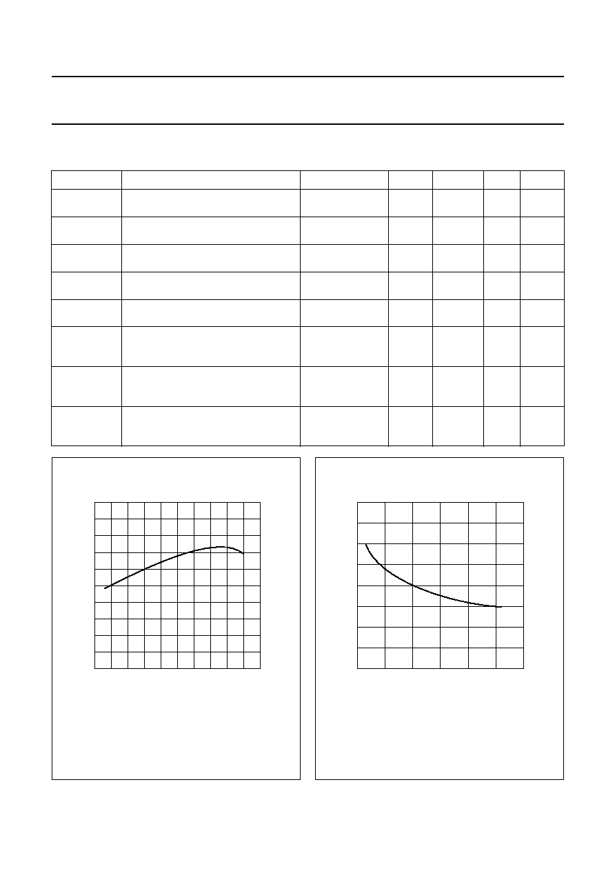
Fig.3
DC current gain as a function of collector
current, typical values.
V
CE
= 20 V; T
j
= 25
°
C.
handbook, halfpage
0
0.5
IC (A)
hFE
100
0
20
40
60
80
0.1
0.2
0.3
0.4
MBK467
Fig.4
Collector capacitance as a function of
collector-base voltage, typical values.
I
E
= i
e
= 0; f = 1 MHz.
handbook, halfpage
0
10
20
30
VCB (V)
Cc
(pF)
8
6
2
0
4
MBK468
September 1991
5
Philips Semiconductors
Product specification
UHF power transistor
BLV99/SL
APPLICATION INFORMATION
RF performance T
mb
= 25
°
C in a common emitter class-B test circuit.
MODE OF OPERATION
f
(MHz)
V
CE
(V)
P
L
(W)
G
p
(dB)
c
(%)
c.w. narrow band
900
24
2
>
8
typ. 9.3
>
55
typ. 63
Fig.5
Gain and efficiency as functions of load
power, typical values.
Class-B operation; V
CE
= 24 V; f = 900 MHz;
T
mb
= 25
°
C.
handbook, halfpage
10
0
1
3
PL (W)
Gp
(dB)
Gp
C
(%)
C
0
2
5
100
0
50
MBK469
Ruggedness in class-B operation
The BLV99/SL is capable of withstanding a full load
mismatch corresponding to VSWR = 50:1 through all
phases under the following conditions:
V
CE
= 24 V, f = 900 MHz,
T
mb
= 25
°
C, and rated output power.
Fig.6
Load power as a function of drive power,
typical values.
Class-B operation; V
CE
= 24 V; f = 900 MHz;
T
mb
= 25
°
C.
handbook, halfpage
0
3
2
1
0
0.1
0.2
0.4
PS (W)
PL
(W)
0.3
MBK470