Document Outline
- GENERAL DESCRIPTION
- QUICK REFERENCE DATA
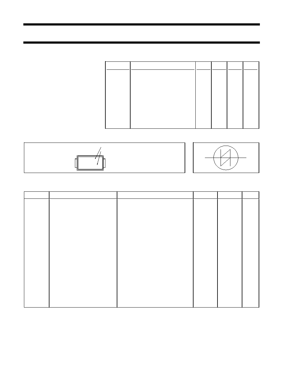
- OUTLINE - SOD106
- SYMBOL
- LIMITING VALUES
- THERMAL RESISTANCES
- ELECTRICAL CHARACTERISTICS
- MECHANICAL DATA
- DEFINITIONS
- LIFE SUPPORT APPLICATIONS
Philips Semiconductors
Product specification
Breakover diodes
BRS212 series
GENERAL DESCRIPTION
QUICK REFERENCE DATA
A range of bidirectional, breakover
SYMBOL
PARAMETER
MIN.
TYP.
MAX.
UNIT
diodes in a two terminal, surface
mounting, plastic envelope. These
V
(BO)
Breakover voltage
devices feature controlled breakover
BRS212-140
-
140
-
V
voltage and high holding current
BRS212-160
-
160
-
V
together with high peak current
BRS212-180
-
180
-
V
handling capability. Their intended
BRS212-200
-
200
-
V
application is protection of line based
BRS212-220
-
220
-
V
telecommunications
equipment
BRS212-240
-
240
-
V
against voltage transients.
BRS212-260
-
260
-
V
BRS212-280
-
280
-
V
I
H
Holding current
150
-
-
mA
I
PP
Non-repetitive peak pulse
-
-
40
A
current (CCITT K17)
OUTLINE - SOD106
SYMBOL
LIMITING VALUES
Limiting values in accordance with the Absolute Maximum System (IEC 134).
SYMBOL
PARAMETER
CONDITIONS
MIN.
MAX.
UNIT
V
D
Continuous voltage
BRS212-140
-
105
V
BRS212-160
-
120
V
BRS212-180
-
135
V
BRS212-200
-
150
V
BRS212-220
-
165
V
BRS212-240
-
180
V
BRS212-260
-
195
V
BRS212-280
-
210
V
I
PP
Non-repetitive peak pulse
5/310
�
s impulse equivalent to
-
40
A
current
10/700
�
s, 1.6 kV voltage impulse
(CCITT K17)
I
TSM
Non repetitive surge peak
half sine wave; t = 10 ms;
-
15
A
on-state current
T
j
= 70 �C prior to surge
I
2
t
I
2
t for fusing
t
p
= 10 ms
-
1.1
A
2
s
dI
T
/dt
Rate of rise of on-state current
t
p
= 10
�
s
-
50
A/
�
s
after V
(BO)
turn-on
P
tot
Continuous dissipation on
T
sp
= 50�C
-
4
W
infinite heatsink
P
TM
Peak dissipation
t
p
= 1 ms; T
a
= 25�C
-
50
W
T
stg
Storage temperature
- 40
150
�C
T
j
Operating junction temperature
-
150
�C
T
L
Maximum terminal temperature soldering time = 10 s
-
260
�C
for soldering
YM
212
XXX
XXX denotes voltage grade
date code
PH
January 1997
1
Rev 1.000

Philips Semiconductors
Product specification
Breakover diodes
BRS212 series
THERMAL RESISTANCES
SYMBOL
PARAMETER
CONDITIONS
MIN.
TYP.
MAX.
UNIT
R
th j-sp
Thermal resistance junction to
-
-
25
K/W
solder point
R
th j-a
Thermal resistance junction to
pcb mounted; minimum footprint
-
100
-
K/W
ambient
Z
th j-a
Thermal impedance junction to
t
p
= 1 ms
-
2.6
-
K/W
ambient
ELECTRICAL CHARACTERISTICS
T
j
= 25 �C unless otherwise stated
TYPE
PARAMETER
Marking
Avalanche
Breakover
Off-state current
Critical rate of
voltage
voltage
rise of off-state
voltage
Conditions
I
BR
= 10 mA
I
D
I
S
T
j
= 70�C;
T
j
= 70�C
t
p
= 100
�
s
RH
65%
Symbol
V
BR
V
BO
I
D
@ V
D
dV
D
/dt @ V
DM
Limits
min
typ
typ
max
max
max
Units
V
V
V
V
�
A
V
V/
�
s
V
BRS212-140
212-140
123
140
140
157
10
105
2000
105
BRS212-160
212-160
140
160
160
180
10
120
2000
120
BRS212-180
212-180
158
180
180
202
10
135
2000
135
BRS212-200
212-200
176
200
200
224
10
150
2000
150
BRS212-220
212-220
193
220
220
247
10
165
2000
165
BRS212-240
212-240
211
240
240
269
10
180
2000
180
BRS212-260
212-260
228
260
260
292
10
195
2000
195
BRS212-280
212-280
246
280
280
314
10
210
2000
210
SYMBOL
PARAMETER
CONDITIONS
MIN.
TYP.
MAX.
UNIT
V
T
On-state voltage
I
TM
= 2 A; t
p
= 200
�
s
-
-
2.5
V
I
H
Holding current
1
T
j
= 25�C
150
-
-
mA
T
j
= 70�C
100
-
-
mA
I
S
Switching current
2
t
p
= 100
�
s
10
200
1000
mA
S
(BR)
Temperature coefficient of
-
+0.1
-
%/K
avalanche voltage
C
j
Junction capacitance
V
D
= 0 V, f = 1 kHz to 1 MHz
-
-
100
pF
1 The minimum current at which the diode will remain in the on-state
2 The avalanche current required to switch the diode to the on-state.
January 1997
2
Rev 1.000
Philips Semiconductors
Product specification
Breakover diodes
BRS212 series
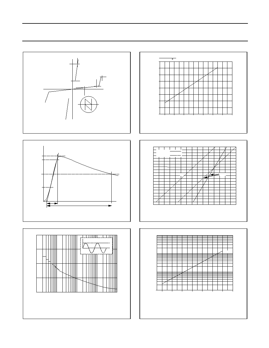
Fig.1. Definition of breakover diode characteristics.
Fig.2. Test waveform for high voltage impulse (I
PP
)
according to CCITT vol IX-Rec K17.
Fig.3. Maximum permissible non-repetitive on-state
current based on sinusoidal currents; f = 50 Hz;
device triggered at the start of each pulse; T
j
= 70�C
prior to surge.
Fig.4. Normalised avalanche breakdown voltage V
(BR)
and V
(BO)
as a function of temperature.
Fig.5. On-state current as a function of on-state
voltage; t
p
= 200
�
s to avoid excessive dissipation.
Fig.6. Maximum off-state current as a function of
temperature.
VT
IT
IH
V(BO)
IS
ID
VD
current
voltage
Symbol
V(BR)
I(BR)
Symmetric BOD
-40
-20
0
20
40
60
80
100
Tj / C
V(BR)(Tj)
1.06
1.04
1.02
1.00
0.98
0.96
0.94
0.92
0.90
V(BR)(25 C)
100%
90%
50%
30%
I
5us
310us
time
current
0
PP
1
2
3
4
0
5
10
15
20
Tj = 25 C
Tj = 150 C
IT / A
VT / V
typ
max
1
10
100
1000
10000
0
5
10
15
20
BR211
Number of impulses
ITSM / A
I
ITSM
time
-40
-20
0
20
40
60
80
100
Tj / C
ID / uA
0.1
1
10
100
max
January 1997
3
Rev 1.000
Philips Semiconductors
Product specification
Breakover diodes
BRS212 series
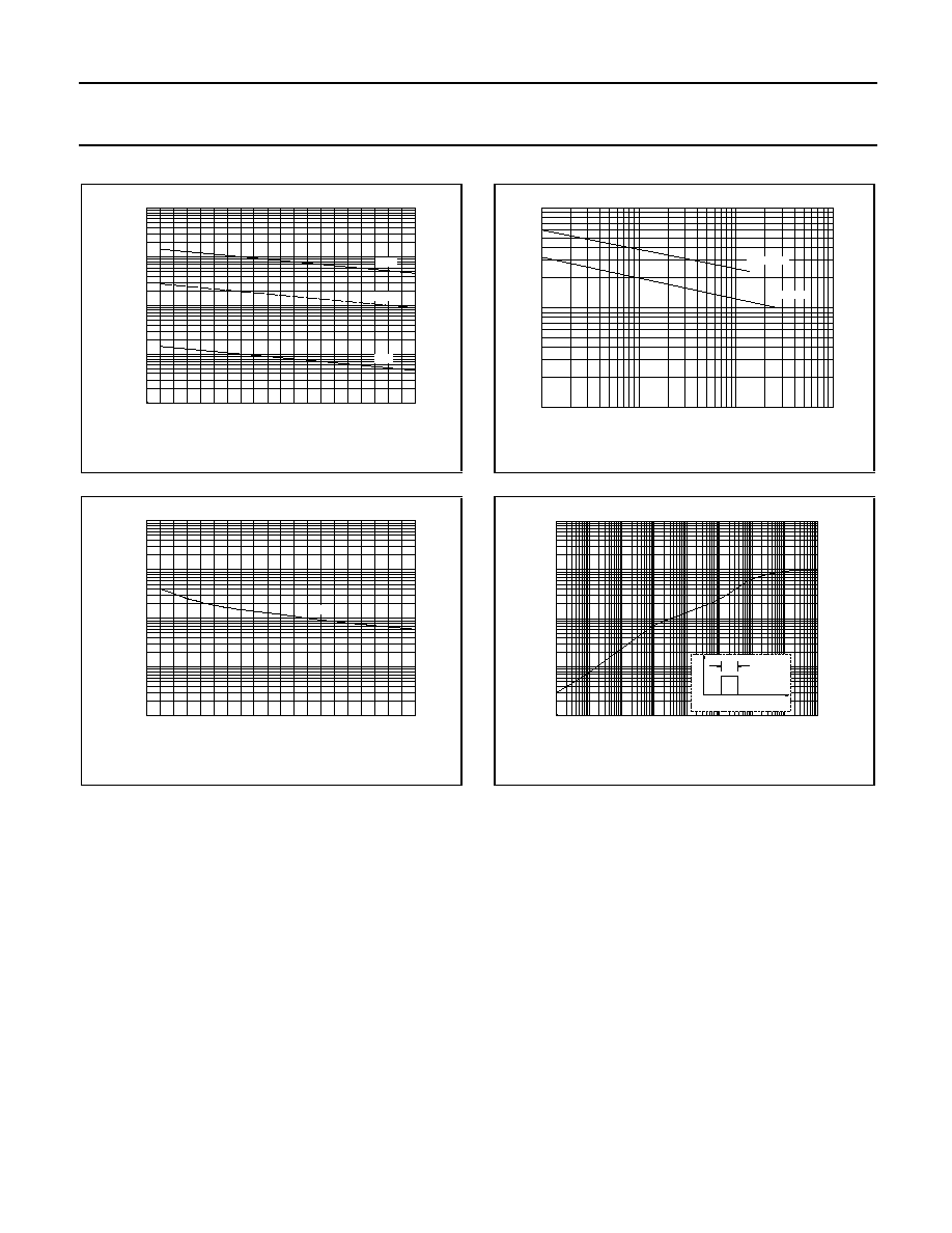
Fig.7. Switching current as a function of junction
temperature.
Fig.8. Minimum holding current as a function of
temperature.
Fig.9. Typical junction capacitance as a function of
off-state voltage, f = 1 MHz; T
j
= 25�C.
Fig.10. Transient thermal impedance. Z
th
j-a
= f(t
p
).
-50
0
50
150
Tj / C
IS / A
0.001
0.01
0.1
10
100
1
max
typ
min
VD / V
1
10
100
1000
1
10
100
Cj / pF
BR211-280
BR211-140
typ
-50
0
50
150
Tj / C
IH / A
0.001
0.01
0.1
10
100
1
min
t
p
P
t
D
Zth / (K/W)
0.1
1
10
100
1000
10us
1ms
0.1s
10s
1000s
tp / s
BR211
January 1997
4
Rev 1.000
Philips Semiconductors
Product specification
Breakover diodes
BRS212 series
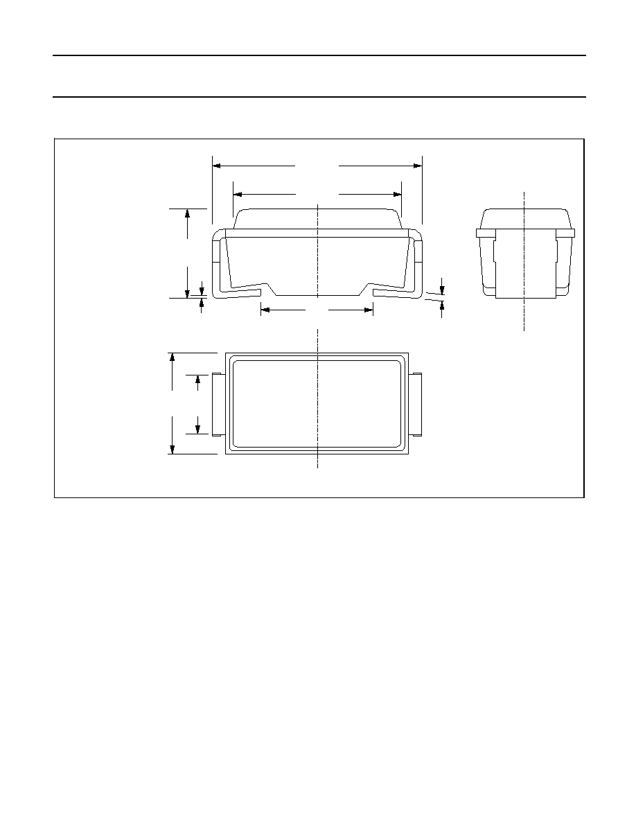
MECHANICAL DATA
Dimensions in mm
Net Mass: 0.2 g
Fig.11. SOD106.
Notes
1. For mounting and soldering instructions refer to publication SC18 "SMD Footprint Design and Soldering
Guidelines". Order code:9397 750 00505.
3.3
2.7
0.2
5.5
5.1
4.5
4.3
2.3
2.0
0.05
2.8
2.4
1.6
1.4
January 1997
5
Rev 1.000