 | –≠–ª–µ–∫—Ç—Ä–æ–Ω–Ω—ã–π –∫–æ–º–ø–æ–Ω–µ–Ω—Ç: BSH205 | –°–∫–∞—á–∞—Ç—å:  PDF PDF  ZIP ZIP |
Philips Semiconductors
Product specification
P-channel enhancement mode
BSH205
MOS transistor
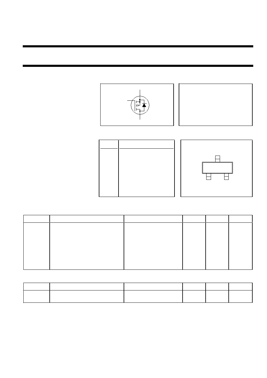
FEATURES
SYMBOL
QUICK REFERENCE DATA
∑ Very low threshold voltage
V
DS
= -12 V
∑ Fast switching
∑ Logic level compatible
I
D
= -0.75 A
∑ Subminiature surface mount
package
R
DS(ON)
0.5
(V
GS
= -2.5 V)
V
GS(TO)
0.4 V
GENERAL DESCRIPTION
PINNING
SOT23
P-channel, enhancement mode,
PIN
DESCRIPTION
logic
level,
field-effect
power
transistor. This device has low
1
gate
threshold voltage and extremely
fast switching making it ideal for
2
source
battery powered applications and
high speed digital interfacing.
3
drain
The BSH205 is supplied in the
SOT23
subminiature
surface
mounting package.
LIMITING VALUES
Limiting values in accordance with the Absolute Maximum System (IEC 134)
SYMBOL
PARAMETER
CONDITIONS
MIN.
MAX.
UNIT
V
DS
Drain-source voltage
-
-12
V
V
DGR
Drain-gate voltage
R
GS
= 20 k
-
-12
V
V
GS
Gate-source voltage
-
±
8
V
I
D
Drain current (DC)
T
a
= 25 ∞C
-
-0.75
A
T
a
= 100 ∞C
-
-0.47
A
I
DM
Drain current (pulse peak value)
T
a
= 25 ∞C
-
-3
A
P
tot
Total power dissipation
T
a
= 25 ∞C
-
0.417
W
T
a
= 100 ∞C
-
0.17
W
T
stg
, T
j
Storage & operating temperature
- 55
150
∞C
THERMAL RESISTANCES
SYMBOL
PARAMETER
CONDITIONS
TYP.
MAX.
UNIT
R
th j-a
Thermal resistance junction to
FR4 board, minimum
300
-
K/W
ambient
footprint
d
g
s
1
2
3
Top view
August 1998
1
Rev 1.000

Philips Semiconductors
Product specification
P-channel enhancement mode
BSH205
MOS transistor
ELECTRICAL CHARACTERISTICS
T
j
= 25∞C unless otherwise specified
SYMBOL PARAMETER
CONDITIONS
MIN.
TYP. MAX. UNIT
V
(BR)DSS
Drain-source breakdown
V
GS
= 0 V; I
D
= -10
µ
A
-12
-
-
V
voltage
V
GS(TO)
Gate threshold voltage
V
DS
= V
GS
; I
D
= -1 mA
-0.4
-0.68
-
V
T
j
= 150∞C
-0.1
-
-
V
R
DS(ON)
Drain-source on-state
V
GS
= -4.5 V; I
D
= -430 mA
-
0.18
0.4
resistance
V
GS
= -2.5 V; I
D
= -430 mA
-
0.32
0.5
V
GS
= -1.8 V; I
D
= -210 mA
-
0.42
0.6
V
GS
= -2.5 V; I
D
= -430 mA; T
j
= 150∞C
-
0.48
0.75
g
fs
Forward transconductance
V
DS
= -9.6 V; I
D
= -430 mA
0.5
1.6
-
S
I
GSS
Gate source leakage current V
GS
=
±
8 V; V
DS
= 0 V
-
±
10
±
100
nA
I
DSS
Zero gate voltage drain
V
DS
= -9.6 V; V
GS
= 0 V;
-
-50
-100
nA
current
T
j
= 150∞C
-
-11
-100
µ
A
Q
g(tot)
Total gate charge
I
D
= -0.5 A; V
DD
= -10 V; V
GS
= -4.5 V
-
3.8
-
nC
Q
gs
Gate-source charge
-
0.4
-
nC
Q
gd
Gate-drain (Miller) charge
-
1.0
-
nC
t
d on
Turn-on delay time
V
DD
= -10 V; I
D
= -0.5 A;
-
2
-
ns
t
r
Turn-on rise time
V
GS
= -8 V; R
G
= 6
-
4.5
-
ns
t
d off
Turn-off delay time
Resistive load
-
45
-
ns
t
f
Turn-off fall time
-
20
-
ns
C
iss
Input capacitance
V
GS
= 0 V; V
DS
= -9.6 V; f = 1 MHz
-
200
-
pF
C
oss
Output capacitance
-
95
-
pF
C
rss
Feedback capacitance
-
41
-
pF
REVERSE DIODE LIMITING VALUES AND CHARACTERISTICS
T
j
= 25∞C unless otherwise specified
SYMBOL
PARAMETER
CONDITIONS
MIN.
TYP.
MAX.
UNIT
I
DR
Continuous reverse drain
T
a
= 25 ∞C
-
-
-0.75
A
current
I
DRM
Pulsed reverse drain current
-
-
-3
A
V
SD
Diode forward voltage
I
F
= -0.38 A; V
GS
= 0 V
-
-0.72
-1.3
V
t
rr
Reverse recovery time
I
F
= -0.5 A; -dI
F
/dt = 100 A/
µ
s;
-
75
-
ns
Q
rr
Reverse recovery charge
V
GS
= 0 V; V
R
= -9.6 V
-
69
-
nC
August 1998
2
Rev 1.000

Philips Semiconductors
Product specification
P-channel enhancement mode
BSH205
MOS transistor
Fig.1. Normalised power dissipation.
PD% = 100
P
D
/P
D 25 ∞C
= f(T
a
)
Fig.2. Normalised continuous drain current.
ID% = 100
I
D
/I
D 25 ∞C
= f(T
a
); conditions: V
GS
-10 V
Fig.3. Safe operating area. T
a
= 25 ∞C
I
D
& I
DM
= f(V
DS
); I
DM
single pulse; parameter t
p
Fig.4. Transient thermal impedance.
Z
th j-a
= f(t); parameter D = t
p
/T
Fig.5. Typical output characteristics, T
j
= 25 ∞C.
I
D
= f(V
DS
); parameter V
GS
Fig.6. Typical on-state resistance, T
j
= 25 ∞C.
R
DS(ON)
= f(I
D
); parameter V
GS
Normalised Power Dissipation, PD (%)
0
20
40
60
80
100
120
0
25
50
75
100
125
150
Ambient Temperature, Ta (C)
BSH105
0.1
1
10
100
1000
1E-06
1E-05
1E-04
1E-03
1E-02
1E-01
1E+00
1E+01
Pulse width, tp (s)
Peak Pulsed Drain Current, IDM (A)
single pulse
D = 0.5
0.2
0.1
0.05
0.02
tp
D = tp/T
D
P
T
Normalised Drain Current, ID (%)
0
20
40
60
80
100
120
0
25
50
75
100
125
150
Ambient Temperature, Ta (C)
BSH205
-1.4
-1.2
-1
-0.8
-0.6
-0.4
-0.2
0
-2
-1.5
-1
-0.5
0
Drain-Source Voltage, VDS (V)
Drain current, ID (A)
-0.9 V
-1.1 V
4.5 V
-1.8 V
-1 V
Tj = 25 C
-1.2 V
-1.3 V
VGS = -1.4 V
-2.5 V
BSH205
0.01
0.1
1
10
100
0.1
1
10
100
Drain-Source Voltage, VDS (V)
Peak Pulsed Drain Current, IDM (A)
d.c.
100 ms
10 ms
RDS(on) = VDS/ ID
tp = 100 us
1 ms
BSH205
0
0.2
0.4
0.6
0.8
1
1.2
1.4
1.6
1.8
2
2.2
2.4
2.6
2.8
3
-1.4
-1.2
-1
-0.8
-0.6
-0.4
-0.2
0
Drain Current, ID (A)
Drain-Source On Resistance, RDS(on) (Ohms)
VGS = -4.5V
-1.2 V
-1V
Tj = 25 C
-1.4 V
-1.1 V
-0.9 V
-2.5 V
-1.3 V
-1.8 V
August 1998
3
Rev 1.000

Philips Semiconductors
Product specification
P-channel enhancement mode
BSH205
MOS transistor
Fig.7. Typical transfer characteristics.
I
D
= f(V
GS
)
Fig.8. Typical transconductance, T
j
= 25 ∞C.
g
fs
= f(I
D
)
Fig.9. Normalised drain-source on-state resistance.
R
DS(ON)
/R
DS(ON)25 ∞C
= f(T
j
)
Fig.10. Gate threshold voltage.
V
GS(TO)
= f(T
j
); conditions: I
D
= 1 mA; V
DS
= V
GS
Fig.11. Sub-threshold drain current.
I
D
= f(V
GS)
; conditions: T
j
= 25 ∞C
Fig.12. Typical capacitances, C
iss
, C
oss
, C
rss
.
C = f(V
DS
); conditions: V
GS
= 0 V; f = 1 MHz
BSH205
-3
-2.5
-2
-1.5
-1
-0.5
0
-3
-2.5
-2
-1.5
-1
-0.5
0
Gate-Source Voltage, VGS (V)
VDS > ID X RDS(on)
Tj = 25 C
150 C
Drain Current, ID (A)
Threshold Voltage, VGS(to), (V)
0
0.1
0.2
0.3
0.4
0.5
0.6
0.7
0
25
50
75
100
125
150
Junction Temperature, Tj (C)
minimum
typical
BSH205
0
0.5
1
1.5
2
2.5
3
3.5
-2.6
-2.4
-2.2
-2
-1.8
-1.6
-1.4
-1.2
-1
-0.8
-0.6
-0.4
-0.2
0
Drain Current, ID (A)
Transconductance, gfs (S)
Tj = 25 C
150 C
VDS > ID X RDS(on)
BSH205
1E-07
1E-06
1E-05
1E-04
1E-03
1E-02
1E-01
-1
-0.9 -0.8 -0.7 -0.6 -0.5 -0.4 -0.3 -0.2 -0.1
0
Gate-Source Voltage, VGS (V)
Drain Current, ID (A)
VDS = -5 V
Tj = 25 C
Normalised Drain-Source On Resistance
0.5
0.6
0.7
0.8
0.9
1
1.1
1.2
1.3
1.4
1.5
1.6
1.7
1.8
1.9
2
0
25
50
75
100
125
150
Junction Temperature, Tj (C)
VGS = -4.5 V
-1.8 V
RDS(ON) @ Tj
RDS(ON) @ 25C
-2.5 V
BSH205
10
100
1000
-0.1
-1.0
-10.0
-100.0
Drain-Source Voltage, VDS (V)
Capacitances, Ciss, Coss, Crss (pF)
Ciss
Coss
Crss
August 1998
4
Rev 1.000

Philips Semiconductors
Product specification
P-channel enhancement mode
BSH205
MOS transistor
Fig.13. Typical turn-on gate-charge characteristics.
V
GS
= f(Q
G
)
Fig.14. Typical reverse diode current.
I
F
= f(V
SDS
); conditions: V
GS
= 0 V; parameter T
j
BSH205
-6
-5
-4
-3
-2
-1
0
0
1
2
3
4
5
Gate charge, (nC)
Gate-source voltage, VGS (V)
VDD = 10 V
RD = 20 Ohms
Tj = 25 C
BSH205
0
0.5
1
1.5
2
2.5
3
3.5
4
4.5
5
0
0.2
0.4
0.6
0.8
1
1.2
1.4
Drain-Source Voltage, VSDS (V)
Source-Drain Diode Current, IF (A)
Tj = 25 C
150 C
August 1998
5
Rev 1.000