 | –≠–ª–µ–∫—Ç—Ä–æ–Ω–Ω—ã–π –∫–æ–º–ø–æ–Ω–µ–Ω—Ç: BST60 | –°–∫–∞—á–∞—Ç—å:  PDF PDF  ZIP ZIP |

DATA SHEET
Product specification
Supersedes data of 1997 Apr 16
1999 Apr 27
DISCRETE SEMICONDUCTORS
BST60; BST61; BST62
PNP Darlington transistors
book, halfpage
M3D109

1999 Apr 27
2
Philips Semiconductors
Product specification
PNP Darlington transistors
BST60; BST61; BST62
FEATURES
∑
High current (max. 0.5 A)
∑
Low voltage (max. 80 V)
∑
Integrated diode and resistor.
APPLICATIONS
∑
Industrial switching applications such as:
≠ Print hammer
≠ Solenoid
≠ Relay and lamp driving.
DESCRIPTION
PNP Darlington transistor in a SOT89 plastic package.
NPN complements: BST50, BST51 and BST52.
MARKING
TYPE NUMBER
MARKING CODE
BST60
BS1
BST61
BS2
BST62
BS3
PINNING
PIN
DESCRIPTION
1
emitter
2
collector
3
base
Fig.1 Simplified outline (SOT89) and symbol.
handbook, halfpage
1
2
3
MAM326
Bottom view
3
2
1

1999 Apr 27
3
Philips Semiconductors
Product specification
PNP Darlington transistors
BST60; BST61; BST62
LIMITING VALUES
In accordance with the Absolute Maximum Rating System (IEC 134).
Note
1. Device mounted on a printed-circuit board, single sided copper, tinplated, mounting pad for collector 6 cm
2
.
For other mounting conditions, see
"Thermal considerations for SOT89 in the General Part of associated Handbook".
SYMBOL
PARAMETER
CONDITIONS
MIN.
MAX.
UNIT
V
CBO
collector-base voltage
open emitter
BST60
-
-
60
V
BST61
-
-
80
V
BST62
-
-
90
V
V
CES
collector-emitter voltage
V
BE
= 0
BST60
-
-
45
V
BST61
-
-
60
V
BST62
-
-
80
V
V
EBO
emitter-base voltage
open collector
-
-
5
V
I
C
collector current (DC)
-
-
0.5
A
I
CM
peak collector current
-
-
1.5
A
I
B
base current (DC)
-
-
100
mA
P
tot
total power dissipation
T
amb
25
∞
C; note 1
-
1.3
W
T
stg
storage temperature
-
65
+150
∞
C
T
j
junction temperature
-
150
∞
C
T
amb
operating ambient temperature
-
65
+150
∞
C

1999 Apr 27
4
Philips Semiconductors
Product specification
PNP Darlington transistors
BST60; BST61; BST62
THERMAL CHARACTERISTICS
Note
1. Device mounted on a printed-circuit board, single sided copper, tinplated, mounting pad for collector 6 cm
2
.
For other mounting conditions, see
"Thermal considerations for SOT89 in the General Part of associated Handbook".
CHARACTERISTICS
T
j
= 25
∞
C unless otherwise specified.
Note
1. Pulse test: t
p
300
µ
s;
0.02.
SYMBOL
PARAMETER
CONDITIONS
VALUE
UNIT
R
th j-a
thermal resistance from junction to ambient
note 1
96
K/W
R
th j-s
thermal resistance from junction to soldering point
16
K/W
SYMBOL
PARAMETER
CONDITIONS
MIN.
TYP.
MAX.
UNIT
I
CES
collector cut-off current
BST60
V
BE
= 0; V
CE
=
-
45 V
-
-
-
50
nA
BST61
V
BE
= 0; V
CE
=
-
60 V
-
-
-
50
nA
BST62
V
BE
= 0; V
CE
=
-
80 V
-
-
-
50
nA
I
EBO
emitter cut-off current
I
C
= 0; V
EB
=
-
4 V
-
-
-
50
nA
h
FE
DC current gain
V
CE
=
-
10 V; note 1; see Fig.2
I
C
=
-
150 mA
1000
-
-
I
C
=
-
500 mA
2000
-
-
V
CEsat
collector-emitter saturation
voltage
I
C
=
-
500 mA; I
B
=
-
0.5 mA
-
-
-
1.3
V
I
C
=
-
500 mA; I
B
=
-
0.5 mA; T
j
= 150
∞
C
-
-
-
1.3
V
V
BEsat
base-emitter saturation
voltage
I
C
=
-
500 mA; I
B
=
-
0.5 mA
-
-
-
1.9
V
f
T
transition frequency
I
C
=
-
500 mA; V
CE
=
-
5 V; f = 100 MHz
-
200
-
MHz
Switching times (between 10% and 90% levels); see Fig.3
t
on
turn-on time
I
Con
=
-
500 mA; I
Bon
=
-
0.5 mA;
I
Boff
= 0.5 mA
-
500
-
ns
t
off
turn-off time
-
700
-
ns
1999 Apr 27
5
Philips Semiconductors
Product specification
PNP Darlington transistors
BST60; BST61; BST62
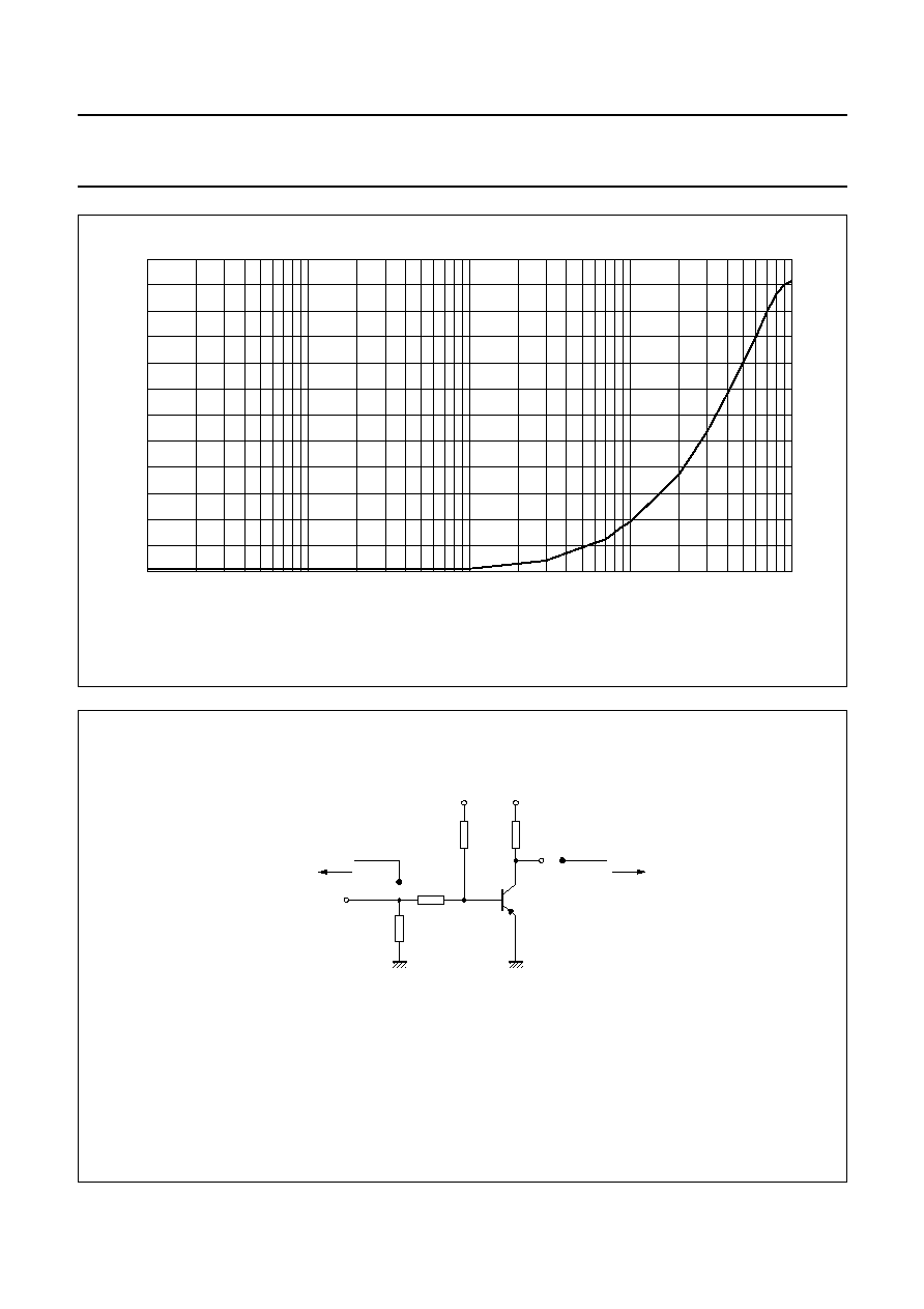
Fig.2 DC current gain; typical values.
handbook, full pagewidth
0
6000
2000
1000
3000
4000
5000
MGD839
-
10
-
1
-
1
-
10
-
10
2
-
10
3
hFE
IC (mA)
V
CE
=
-
10 V.
Fig.3 Test circuit for switching times.
handbook, full pagewidth
RC
R2
R1
DUT
MGD624
Vo
RB
(probe)
450
(probe)
450
oscilloscope
oscilloscope
VBB
Vi
VCC
V
i
=
-
10 V; T = 200
µ
s; t
p
= 6
µ
s; t
r
= t
f
3 ns.
R1 = 56
; R2 = 10 k
; R
B
= 10 k
; R
C
= 18
.
V
BB
= 1.8 V; V
CC
=
-
10.7 V.
Oscilloscope: input impedance Z
i
= 50
.