
Philips Semiconductors
Product specification
Triacs
BT134W series
GENERAL DESCRIPTION
QUICK REFERENCE DATA
Glass passivated triacs in a plastic
SYMBOL
PARAMETER
MAX.
MAX.
MAX. UNIT
envelope
suitable
for
surface
mounting,
intended
for
use
in
BT134W-
500
600
800
applications
requiring
high
BT134W-
500F
600F
800F
bidirectional transient and blocking
BT134W-
500G
600G
800G
voltage capability and high thermal
V
DRM
Repetitive peak off-state
500
600
800
V
cycling
performance.
Typical
voltages
applications include motor control,
I
T(RMS)
RMS on-state current
1
1
1
A
industrial
and
domestic
lighting,
I
TSM
Non-repetitive peak on-state
10
10
10
A
heating and static switching.
current
PINNING - SOT223
PIN CONFIGURATION
SYMBOL
PIN
DESCRIPTION
1
main terminal 1
2
main terminal 2
3
gate
tab
main terminal 2
LIMITING VALUES
Limiting values in accordance with the Absolute Maximum System (IEC 134).
SYMBOL
PARAMETER
CONDITIONS
MIN.
MAX.
UNIT
-500
-600
-800
V
DRM
Repetitive peak off-state
-
500
1
600
1
800
V
voltages
I
T(RMS)
RMS on-state current
full sine wave; T
sp
108 ∞C
-
1
A
I
TSM
Non-repetitive peak
full sine wave; T
j
= 25 ∞C prior to
on-state current
surge
t = 20 ms
-
10
A
t = 16.7 ms
-
11
A
I
2
t
I
2
t for fusing
t = 10 ms
-
0.5
A
2
s
dI
T
/dt
Repetitive rate of rise of
I
TM
= 1.5 A; I
G
= 0.2 A;
on-state current after
dI
G
/dt = 0.2 A/
µ
s
triggering
T2+ G+
-
50
A/
µ
s
T2+ G-
-
50
A/
µ
s
T2- G-
-
50
A/
µ
s
T2- G+
-
10
A/
µ
s
I
GM
Peak gate current
-
2
A
V
GM
Peak gate voltage
-
5
V
P
GM
Peak gate power
-
5
W
P
G(AV)
Average gate power
over any 20 ms period
-
0.5
W
T
stg
Storage temperature
-40
150
∞C
T
j
Operating junction
-
125
∞C
temperature
T1
T2
G
4
1
2
3
1 Although not recommended, off-state voltages up to 800V may be applied without damage, but the triac may
switch to the on-state. The rate of rise of current should not exceed 3 A/
µ
s.
September 1997
1
Rev 1.200

Philips Semiconductors
Product specification
Triacs
BT134W series
THERMAL RESISTANCES
SYMBOL
PARAMETER
CONDITIONS
MIN.
TYP.
MAX.
UNIT
R
th j-sp
Thermal resistance
full or half cycle
-
-
15
K/W
junction to solder point
R
th j-a
Thermal resistance
pcb mounted; minimum footprint
-
156
-
K/W
junction to ambient
pcb mounted; pad area as in fig:14
-
70
-
K/W
STATIC CHARACTERISTICS
T
j
= 25 ∞C unless otherwise stated
SYMBOL
PARAMETER
CONDITIONS
MIN.
TYP.
MAX.
UNIT
BT134W-
...
...F
...G
I
GT
Gate trigger current
V
D
= 12 V; I
T
= 0.1 A
T2+ G+
-
5
35
25
50
mA
T2+ G-
-
8
35
25
50
mA
T2- G-
-
11
35
25
50
mA
T2- G+
-
30
70
70
100
mA
I
L
Latching current
V
D
= 12 V; I
GT
= 0.1 A
T2+ G+
-
7
20
20
30
mA
T2+ G-
-
16
30
30
45
mA
T2- G-
-
5
20
20
30
mA
T2- G+
-
7
30
30
45
mA
I
H
Holding current
V
D
= 12 V; I
GT
= 0.1 A
-
5
15
15
30
mA
V
T
On-state voltage
I
T
= 2 A
-
1.2
1.50
V
V
GT
Gate trigger voltage
V
D
= 12 V; I
T
= 0.1 A
-
0.7
1.5
V
V
D
= 400 V; I
T
= 0.1 A;
0.25
0.4
-
V
T
j
= 125 ∞C
I
D
Off-state leakage current
V
D
= V
DRM(max)
;
-
0.1
0.5
mA
T
j
= 125 ∞C
DYNAMIC CHARACTERISTICS
T
j
= 25 ∞C unless otherwise stated
SYMBOL
PARAMETER
CONDITIONS
MIN.
TYP.
MAX.
UNIT
BT134W-
...
...F
...G
dV
D
/dt
Critical rate of rise of
V
DM
=67% V
DRM(max)
;
100
50
200
250
-
V/
µ
s
off-state voltage
T
j
= 125 ∞C; exponential
waveform; gate open
circuit
dV
com
/dt
Critical rate of change of
V
DM
= 400 V; T
j
= 95 ∞C;
-
-
10
50
-
V/
µ
s
commutating voltage
I
T(RMS)
= 1 A;
dI
com
/dt = 1.8 A/ms; gate
open circuit
t
gt
Gate controlled turn-on
I
TM
= 1.5 A;
-
-
-
2
-
µ
s
time
V
D
= V
DRM(max)
; I
G
= 0.1 A;
dI
G
/dt = 5 A/
µ
s;
September 1997
2
Rev 1.200

Philips Semiconductors
Product specification
Triacs
BT134W series
Fig.1. Maximum on-state dissipation, P
tot
, versus rms
on-state current, I
T(RMS)
, where
= conduction angle.
Fig.2. Maximum permissible non-repetitive peak
on-state current I
TSM
, versus pulse width t
p
, for
sinusoidal currents, t
p
20ms.
Fig.3. Maximum permissible non-repetitive peak
on-state current I
TSM
, versus number of cycles, for
sinusoidal currents, f = 50 Hz.
Fig.4. Maximum permissible rms current I
T(RMS)
,
versus solder point temperature T
sp
.
Fig.5. Maximum permissible repetitive rms on-state
current I
T(RMS)
, versus surge duration, for sinusoidal
currents, f = 50 Hz; T
sp
108∞C.
Fig.6. Normalised gate trigger voltage
V
GT
(T
j
)/ V
GT
(25∞C), versus junction temperature T
j
.
0
0.2
0.4
0.6
0.8
1
1.2
0
0.2
0.4
0.6
0.8
1
1.2
1.4
= 180
120
90
60
30
BT134W
IT(RMS) / A
Ptot / W
Tsp(max) / C
125
122
119
116
113
110
107
104
1
-50
0
50
100
150
0
0.2
0.4
0.6
0.8
1
1.2
BT134W
Tsp / C
IT(RMS) / A
108 C
1
10
100
1000
BT134W
T / s
ITSM / A
10us
100us
1ms
10ms
100ms
T
ITSM
time
I
Tj initial = 25 C max
T
dI /dt limit
T
T2- G+ quadrant
0.01
0.1
1
10
0
0.5
1
1.5
2
BT134W
surge duration / s
IT(RMS) / A
1
10
100
1000
0
2
4
6
8
10
12
BT134W
Number of cycles at 50Hz
ITSM / A
T
ITSM
time
I
Tj initial = 25 C max
T
-50
0
50
100
150
0.4
0.6
0.8
1
1.2
1.4
1.6
BT136
Tj / C
VGT(Tj)
VGT(25 C)
September 1997
3
Rev 1.200

Philips Semiconductors
Product specification
Triacs
BT134W series
Fig.7. Normalised gate trigger current
I
GT
(T
j
)/ I
GT
(25∞C), versus junction temperature T
j
.
Fig.8. Normalised latching current I
L
(T
j
)/ I
L
(25∞C),
versus junction temperature T
j
.
Fig.9. Normalised holding current I
H
(T
j
)/ I
H
(25∞C),
versus junction temperature T
j
.
Fig.10. Typical and maximum on-state characteristic.
Fig.11. Transient thermal impedance Z
th j-sp
, versus
pulse width t
p
.
Fig.12. Typical commutation dV/dt versus junction
temperature, parameter commutation dI
T
/dt. The triac
should commutate when the dV/dt is below the value
on the appropriate curve for pre-commutation dI
T
/dt.
-50
0
50
100
150
0
0.5
1
1.5
2
2.5
3
BT136
Tj / C
T2+ G+
T2+ G-
T2- G-
T2- G+
IGT(Tj)
IGT(25 C)
0
0.5
1
1.5
2
0
0.5
1
1.5
2
BT134W
VT / V
IT / A
Tj = 125 C
typ
max
Tj = 25 C
Vo = 1.0 V
Rs = 0.21 Ohms
-50
0
50
100
150
0
0.5
1
1.5
2
2.5
3
TRIAC
Tj / C
IL(Tj)
IL(25 C)
10us
0.1ms
1ms
10ms
0.1s
1s
10s
tp / s
0.01
0.1
1
10
Zth j-sp (K/W)
100
t
p
P
t
D
unidirectional
bidirectional
BT134W
-50
0
50
100
150
0
0.5
1
1.5
2
2.5
3
TRIAC
Tj / C
IH(Tj)
IH(25C)
0
50
100
150
1
10
100
1000
1.8
3
Tj / C
dIcom/dt = 5.1
3.9
2.3
dVcom/dt (V/us)
A/ms
1.4
off-state dV/dt limit
BT134...G SERIES
BT134 SERIES
BT134...F SERIES
September 1997
4
Rev 1.200
Philips Semiconductors
Product specification
Triacs
BT134W series
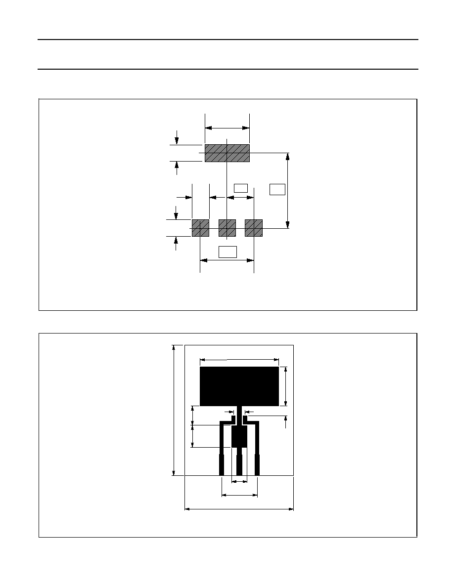
MOUNTING INSTRUCTIONS
Dimensions in mm.
Fig.13. soldering pattern for surface mounting SOT223.
PRINTED CIRCUIT BOARD
Dimensions in mm.
Fig.14. PCB for thermal resistance and power rating for SOT223.
PCB: FR4 epoxy glass (1.6 mm thick), copper laminate (35
µ
m thick).
3.8
min
6.3
2.3
4.6
1.5
min
1.5
min
1.5
min
(3x)
36
60
9
10
4.6
18
4.5
7
15
50
September 1997
5
Rev 1.200