 | –≠–ª–µ–∫—Ç—Ä–æ–Ω–Ω—ã–π –∫–æ–º–ø–æ–Ω–µ–Ω—Ç: BU2508AW | –°–∫–∞—á–∞—Ç—å:  PDF PDF  ZIP ZIP |
Philips Semiconductors
Product specification
Silicon Diffused Power Transistor
BU2508AW
GENERAL DESCRIPTION
Enhanced performance, new generation, high-voltage, high-speed switching npn transistor in a plastic envelope
intended for use in horizontal deflection circuits of colour television receivers. Features exceptional tolerance to
base drive and collector current load variations resulting in a very low worst case dissipation.
QUICK REFERENCE DATA
SYMBOL
PARAMETER
CONDITIONS
TYP.
MAX.
UNIT
V
CESM
Collector-emitter voltage peak value
V
BE
= 0 V
-
1500
V
V
CEO
Collector-emitter voltage (open base)
-
700
V
I
C
Collector current (DC)
-
8
A
I
CM
Collector current peak value
-
15
A
P
tot
Total power dissipation
T
mb
25 ∞C
-
125
W
V
CEsat
Collector-emitter saturation voltage
I
C
= 4.5 A; I
B
= 1.12 A
-
1.0
V
I
Csat
Collector saturation current
f=16kHz
4.5
-
A
t
f
Fall time
I
Csat
= 4.5 A;f=16kHz
0.4
0.6
µ
s
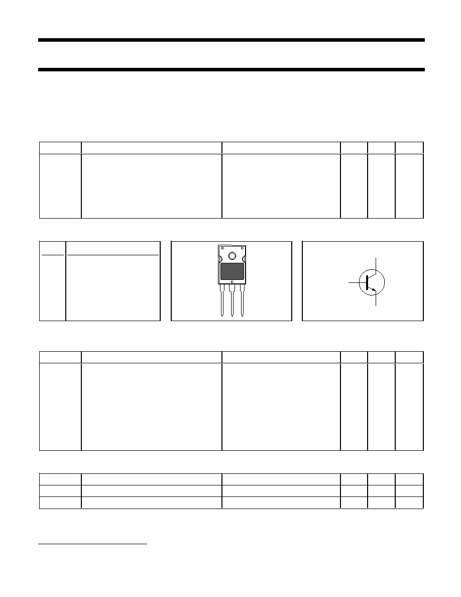
PINNING - SOT429
PIN CONFIGURATION
SYMBOL
PIN
DESCRIPTION
1
base
2
collector
3
emitter
tab
collector
LIMITING VALUES
Limiting values in accordance with the Absolute Maximum Rating System (IEC 134)
SYMBOL
PARAMETER
CONDITIONS
MIN.
MAX.
UNIT
V
CESM
Collector-emitter voltage peak value
V
BE
= 0 V
-
1500
V
V
CEO
Collector-emitter voltage (open base)
-
700
V
I
C
Collector current (DC)
-
8
A
I
CM
Collector current peak value
-
15
A
I
B
Base current (DC)
-
4
A
I
BM
Base current peak value
-
6
A
-I
B(AV)
Reverse base current
average over any 20 ms period
-
100
mA
-I
BM
Reverse base current peak value
1
-
5
A
P
tot
Total power dissipation
T
mb
25 ∞C
-
125
W
T
stg
Storage temperature
-55
150
∞C
T
j
Junction temperature
-
150
∞C
THERMAL RESISTANCES
SYMBOL
PARAMETER
CONDITIONS
TYP.
MAX.
UNIT
R
th j-mb
Junction to mounting base
-
-
1.0
K/W
R
th j-a
Junction to ambient
in free air
45
-
K/W
2
3
1
b
c
e
1 Turn-off current.
September 1997
1
Rev 1.100

Philips Semiconductors
Product specification
Silicon Diffused Power Transistor
BU2508AW
STATIC CHARACTERISTICS
T
mb
= 25 ∞C unless otherwise specified
SYMBOL
PARAMETER
CONDITIONS
MIN.
TYP.
MAX.
UNIT
I
CES
Collector cut-off current
2
V
BE
= 0 V; V
CE
= V
CESMmax
-
-
1.0
mA
I
CES
V
BE
= 0 V; V
CE
= V
CESMmax
;
-
-
2.0
mA
T
j
= 125 ∞C
I
EBO
Emitter cut-off current
V
EB
= 7.5 V; I
C
= 0 A
-
-
1.0
mA
BV
EBO
Emitter-base breakdown voltage
I
B
= 1 mA
7.5
13.5
-
V
V
CEOsust
Collector-emitter sustaining voltage
I
B
= 0 A; I
C
= 100 mA;
700
-
-
V
L = 25 mH
V
CEsat
Collector-emitter saturation voltage
I
C
= 4.5 A; I
B
= 1.12 A
-
-
1.0
V
V
BEsat
Base-emitter saturation voltage
I
C
= 4.5 A; I
B
= 1.7 A
-
-
1.1
V
h
FE
DC current gain
I
C
= 100 mA;V
CE
= 5 V
-
13
-
h
FE
I
C
= 4.5 A;V
CE
= 1 V
4
5.5
7.0
DYNAMIC CHARACTERISTICS
T
mb
= 25 ∞C unless otherwise specified
SYMBOL
PARAMETER
CONDITIONS
TYP.
MAX.
UNIT
C
c
Collector capacitance
I
E
= 0 A; V
CB
= 10 V; f = 1 MHz
80
-
pF
Switching times (16 kHz line
I
Csat
= 4.5 A; I
B(end)
= 1.1 A; L
B
= 6
µ
H;
deflection circuit)
-V
BB
= 4 V; (-dI
B
/dt = 0.6 A/
µ
s)
t
s
Turn-off storage time
5.0
6.0
µ
s
t
f
Turn-off fall time
0.4
0.6
µ
s
Switching times (38 kHz line
I
Csat
= 4.0 A; I
B(end)
= 0.9 A; L
B
= 6
µ
H;
deflection circuit)
-V
BB
= 4 V; (-dI
B
/dt = 0.6 A/
µ
s)
t
s
Turn-off storage time
4.7
5.7
µ
s
t
f
Turn-off fall time
0.25
0.35
µ
s
Fig.1. Test circuit for V
CEO
sust.
Fig.2. Oscilloscope display for V
CEO
sust.
+ 50v
100-200R
Horizontal
Vertical
Oscilloscope
1R
6V
30-60 Hz
100R
VCE / V
min
VCEOsust
IC / mA
100
200
250
0
2 Measured with half sine-wave voltage (curve tracer).
September 1997
2
Rev 1.100

Philips Semiconductors
Product specification
Silicon Diffused Power Transistor
BU2508AW
Fig.3. Switching times waveforms.
Fig.4. Switching times definitions.
Fig.5. Switching times test circuit (BU2508A).
Fig.6. Typical DC current gain. h
FE
= f (I
C
)
parameter V
CE
Fig.7. Typical base-emitter saturation voltage.
V
BE
sat = f (I
C
); parameter I
C
/I
B
Fig.8. Typical collector-emitter saturation voltage.
V
CE
sat = f (I
C
); parameter I
C
/I
B
IC
IB
VCE
ICsat
IBend
64us
26us
20us
t
t
t
BU2508A
DIODE
0.01
1
100
10
1
0.1
10
h
IC / A
FE
Tj = 25 C
Tj = 125 C
5V
1V
ICsat
90 %
10 %
tf
ts
IBend
IC
IB
t
t
- IBM
0.1
1
10
IC / A
VBESAT / V
BU2508A
1.2
1.1
1
0.9
0.8
0.7
0.6
0.5
0.4
Tj = 25 C
Tj = 125 C
3
4
5
IC/IB=
+ 150 v nominal
adjust for ICsat
1mH
BY228
12nF
BU2508A
LB
IBend
-VBB
0.1
1
10
IC / A
VCESAT / V
BU2508A
1
0.9
0.8
0.7
0.6
0.5
0.4
0.3
0.2
0.1
0
Tj = 25 C
Tj = 125 C
5
4
3
IC/IB=
September 1997
3
Rev 1.100

Philips Semiconductors
Product specification
Silicon Diffused Power Transistor
BU2508AW
Fig.9. Typical base-emitter saturation voltage.
V
BE
sat = f (I
B
); parameter I
C
Fig.10. Typical collector-emitter saturation voltage.
V
CE
sat = f (I
B
); parameter I
C
Fig.11. Typical turn-off losses. T
j
= 85∞C
Eoff = f (I
B
); parameter I
C
; f = 16 kHz
Fig.12. Typical collector storage and fall time.
ts = f (I
B
); tf = f (I
B
); parameter I
C
; T
j
= 85∞C; f = 16 kHz
Fig.13. Transient thermal impedance.
Z
th j-mb
= f(t); parameter D = t
p
/T
Fig.14. Normalised power dissipation.
PD% = 100
P
D
/P
D 25∞C
= f (T
mb
)
0
1
2
3
4
IB / A
VBESAT / V
BU2508A
1.2
1.1
1
0.9
0.8
0.7
0.6
6A
4.5A
3A
2A
Tj = 25 C
Tj = 125 C
IC=
0.1
1
10
IB / A
ts, tf / us
BU2508A
12
11
10
9
8
7
6
5
4
3
2
1
0
IC =
3.5A
4.5A
tf
ts
0.1
1
10
IB / A
VCESAT / V
BU2508A
10
1
0.1
Tj = 25 C
Tj = 125 C
3A
4.5A
6A
IC=2A
1E-06
1E-04
1E-02
1E+00
t / s
Zth / (K/W)
10
1
0.1
0.01
D = 0
0.02
0.05
0.1
0.2
0.5
D =
t
p
t
p
T
T
P
t
D
0.1
1
10
IB / A
Eoff / uJ
BU2508A
1000
100
10
3.5A
IC = 4.5A
0
20
40
60
80
100
120
140
Tmb / C
PD%
Normalised Power Derating
120
110
100
90
80
70
60
50
40
30
20
10
0
September 1997
4
Rev 1.100

Philips Semiconductors
Product specification
Silicon Diffused Power Transistor
BU2508AW
Fig.15. Forward bias safe operating area. T
mb
= 25∞C
(1)
P
tot
max line.
(2)
Second-breakdown limits
(independent of temperature).
I
Region of DC operation.
II
Extension for repetitive pulse operation.
1
10
100
1000
100
10
1
0.1
0.01
tp =
5 us
10
20
50
100
200
500
1 ms
2
5
10
20
DC
IC / A
VCE / V
ICM max
IC max
= 0.01
II
I
(1)
(2)
September 1997
5
Rev 1.100