
Philips Semiconductors
Product specification
Silicon Diffused Power Transistor
BU4515AF
GENERAL DESCRIPTION
Enhanced performance, new generation, high-voltage, high-speed switching npn transistor in a plastic full-pack
envelope intended for use in horizontal deflection circuits of colour television receivers an p.c monitors. Features
exceptional tolerance to base drive and collector current load variations resulting in a very low worst case
dissipation.
QUICK REFERENCE DATA
SYMBOL
PARAMETER
CONDITIONS
TYP.
MAX.
UNIT
V
CESM
Collector-emitter voltage peak value
V
BE
= 0 V
-
1500
V
V
CEO
Collector-emitter voltage (open base)
-
800
V
I
C
Collector current (DC)
-
9
A
I
CM
Collector current peak value
-
20
A
P
tot
Total power dissipation
T
hs
25 �C
-
45
W
V
CEsat
Collector-emitter saturation voltage
I
C
= 6.0 A; I
B
= 1.5 A
-
3.0
V
I
Csat
Collector saturation current
f = 16kHz
6.0
-
A
f = 64kHz
5.0
-
A
t
f
Fall time
I
Csat
= 6A; f = 16kHz
0.36
0.5
�
s
I
Csat
= 5A;f = 64kHz
0.23
-
�
s
PINNING - SOT199
PIN CONFIGURATION
SYMBOL
PIN
DESCRIPTION
1
base
2
collector
3
emitter
case isolated
LIMITING VALUES
Limiting values in accordance with the Absolute Maximum Rating System (IEC 134)
SYMBOL
PARAMETER
CONDITIONS
MIN.
MAX.
UNIT
V
CESM
Collector-emitter voltage peak value
V
BE
= 0 V
-
1500
V
V
CEO
Collector-emitter voltage (open base)
-
800
V
I
C
Collector current (DC)
-
9
A
I
CM
Collector current peak value
-
20
A
I
B
Base current (DC)
-
5
A
I
BM
Base current peak value
-
7.5
A
-I
BM
Reverse base current peak value
1
-
6
A
P
tot
Total power dissipation
T
hs
25 �C
-
45
W
T
stg
Storage temperature
-55
150
�C
T
j
Junction temperature
-
150
�C
THERMAL RESISTANCES
SYMBOL
PARAMETER
CONDITIONS
TYP.
MAX.
UNIT
R
th j-hs
Junction to heatsink
with heatsink compound
-
2.8
K/W
R
th j-a
Junction to ambient
in free air
35
-
K/W
1
2
3
case
b
c
e
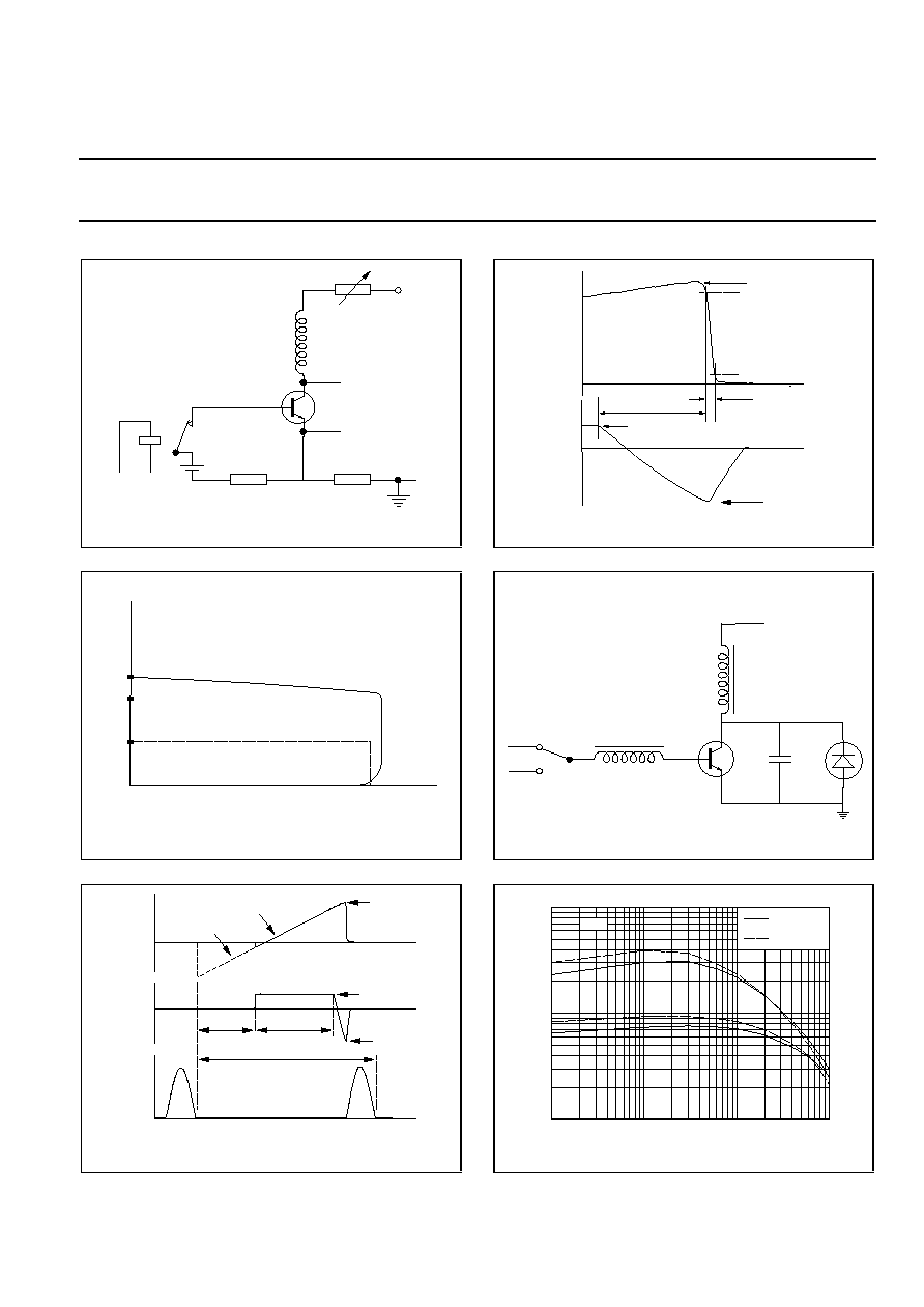
1 Turn-off current.
June 1999
1
Rev 1.000

Philips Semiconductors
Product specification
Silicon Diffused Power Transistor
BU4515AF
ISOLATION LIMITING VALUE & CHARACTERISTIC
T
hs
= 25 �C unless otherwise specified
SYMBOL
PARAMETER
CONDITIONS
MIN.
TYP.
MAX.
UNIT
V
isol
Repetitive peak voltage from all
R.H.
65 % ; clean and dustfree
-
-
2500
V
three terminals to external
heatsink
C
isol
Capacitance from T2 to external f = 1 MHz
-
22
-
pF
heatsink
STATIC CHARACTERISTICS
T
hs
= 25 �C unless otherwise specified
SYMBOL
PARAMETER
CONDITIONS
MIN.
TYP.
MAX.
UNIT
I
CES
Collector cut-off current
2
V
BE
= 0 V; V
CE
= V
CESMmax
-
-
1.0
mA
I
CES
V
BE
= 0 V; V
CE
= V
CESMmax
;
-
-
2.0
mA
T
j
= 125 �C
I
EBO
Emitter cut-off current
V
EB
= 7.5 V,I
C
= 0 A
-
-
1.0
mA
BV
EBO
Emitter-base breakdown voltage
I
B
= 1 mA
7.5
13.5
-
V
V
CEOsust
Collector-emitter sustaining voltage
I
B
= 0 A; I
C
= 100 mA;
800
-
-
V
L = 25 mH
V
CEsat
Collector-emitter saturation voltage
I
C
= 6.0 A; I
B
= 1.5 A
-
-
3.0
V
V
BEsat
Base-emitter saturation voltage
I
C
= 6.0 A; I
B
= 1.5 A
0.85
0.94
1.03
V
h
FE
DC current gain
I
C
= 100 mA; V
CE
= 5 V
-
10
-
h
FE
I
C
= 6 A; V
CE
= 5 V
4.2
5.7
7.3
DYNAMIC CHARACTERISTICS
T
hs
= 25 �C unless otherwise specified
SYMBOL
PARAMETER
CONDITIONS
TYP.
MAX.
UNIT
Switching times (16 kHz line
I
Csat
= 6.0 A;I
B1
= 1.2 A
deflection circuit)
(I
B2
= -3.0 A)
t
s
Turn-off storage time
3.3
4.2
�
s
t
f
Turn-off fall time
0.36
0.5
�
s
Switching times (64 kHz line
I
Csat
= 5.0 A;I
B1
= 1.0 A
deflection circuit)
(I
B2
= -3.3 A)
t
s
Turn-off storage time
1.8
-
�
s
t
f
Turn-off fall time
0.23
-
�
s
2 Measured with half sine-wave voltage (curve tracer).
June 1999
2
Rev 1.000
Philips Semiconductors
Product specification
Silicon Diffused Power Transistor
BU4515AF
Fig.1. Test circuit for V
CEOsust
.
Fig.2. Oscilloscope display for V
CEOsust
.
Fig.3. Switching times waveforms (16 kHz).
Fig.4. Switching times definitions.
Fig.5. Switching times test circuit.
Fig.6. High and low DC current gain.
+ 50v
100-200R
Horizontal
Vertical
Oscilloscope
1R
6V
30-60 Hz
100R
ICsat
90 %
10 %
tf
ts
IB1
IC
IB
t
t
- IB2
VCE / V
min
VCEOsust
IC / mA
100
200
250
0
+ 150 v nominal
adjust for ICsat
Lc
Cfb
T.U.T.
LB
IBend
-VBB
IC
IB
VCE
ICsat
IB1
64us
26us
20us
t
t
t
TRANSISTOR
DIODE
IB2
0.01
0.1
1
10
1
10
100
hFE
IC / A
Ths = 85C
Ths = 25C
1V
June 1999
3
Rev 1.000
Philips Semiconductors
Product specification
Silicon Diffused Power Transistor
BU4515AF
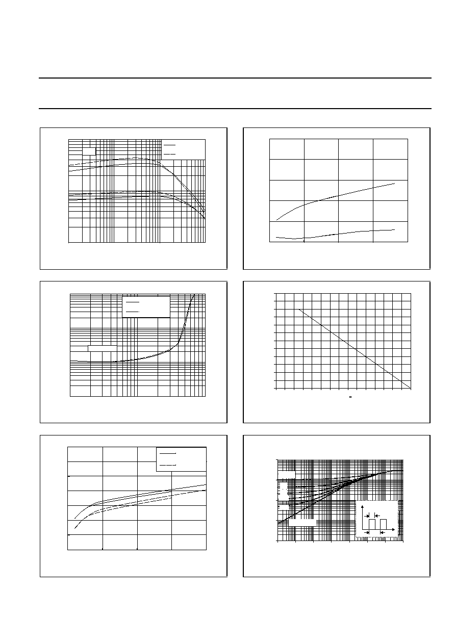
Fig.7. High and low DC current gain.
Fig.8. Typical collector-emitter saturation voltage.
Fig.9. Typical base-emitter saturation voltage.
Fig.10. Typical collector storage and fall time.
I
C
=6 A; T
j
= 85�C; f = 16kHz
Fig.11. Normalised power dissipation.
PD% = 100
P
D
/P
D 25�C
Fig.12. Transient thermal impedance.
0.01
0.1
1
10
1
10
100
Ths = 85C
Ths = 85C
5V
hFE
IC / A
0.5
1
1.5
2
2.5
0
2
4
6
8
10
IB / A
ts/tf/us
ICsat = 6A
Ths 85 C
Freq = 16kHz
0.1
1
10
0.01
0.1
1
10
IC / A
VCEsat / V
Ths = 85C
Ths = 25C
IC/IB = 5
0
20
40
60
80
100
120
140
Ths / C
PD%
Normalised Power Derating
120
110
100
90
80
70
60
50
40
30
20
10
0
with heatsink compound
0
1
2
3
4
0.6
0.7
0.8
0.9
1
1.1
1.2
1.3
IB/A
VBEsat/V
Ths = 25C
Ths = 85C
0.001
0.01
0.1
1
10
1E-06
1E-05
1E-04
1E-03
1E-02
1E-01
1E+00
1E+01
pulse width, tp (s)
Zth / (K/W)
D = 0.5
0.2
0.1
0.05
0.02
Single pulse
tp
D = tp/T
T
P
t
D
June 1999
4
Rev 1.000

Philips Semiconductors
Product specification
Silicon Diffused Power Transistor
BU4515AF
Fig.13. I
Csat
during normal running vs. frequency of
operation for optimum performance
0
20
40
60
80
100
0
2
4
6
8
10
Frequency (kHz)
Ic(sat) (A)
June 1999
5
Rev 1.000