
DATA SHEET
Product specification
August 1998
DISCRETE SEMICONDUCTORS
BUJ103A
Silicon Diffused Power Transistor

August 1998
1
Rev 1.000
Philips Semiconductors
Product specification
Silicon Diffused Power Transistor
BUJ103A
GENERAL DESCRIPTION
High-voltage, high-speed planar-passivated npn power switching transistor in TO220AB envelope intended for use
in high frequency electronic lighting ballast applications, converters, inverters, switching regulators, motor control
systems, etc.
QUICK REFERENCE DATA
SYMBOL
PARAMETER
CONDITIONS
TYP.
MAX.
UNIT
V
CESM
Collector-emitter voltage peak value
V
BE
= 0 V
-
700
V
V
CBO
Collector-Base voltage (open emitter)
-
700
V
V
CEO
Collector-emitter voltage (open base)
-
400
V
I
C
Collector current (DC)
2
-
4
A
I
CM
Collector current peak value
-
8
A
P
tot
Total power dissipation
T
mb
25 �C
-
80
W
V
CEsat
Collector-emitter saturation voltage
I
C
= 3.0 A;I
B
= 0.6 A
0.25
1.0
V
h
FEsat
I
C
= 3.0 A; V
CE
= 5 V
12.5
-
t
f
Fall time
Ic=2A,I
B1
=0.4A
33
80
ns
PINNING - TO220AB
PIN CONFIGURATION
SYMBOL
PIN
DESCRIPTION
1
base
2
collector
3
emitter
tab
collector
LIMITING VALUES
Limiting values in accordance with the Absolute Maximum Rating System (IEC 134)
SYMBOL
PARAMETER
CONDITIONS
MIN.
MAX.
UNIT
V
CESM
Collector to emitter voltage
V
BE
= 0 V
-
700
V
V
CEO
Collector to emitter voltage (open base)
-
400
V
V
CBO
Collector to base voltage (open emitter)
-
700
V
I
C
Collector current (DC)
-
4
A
I
CM
Collector current peak value
-
8
A
I
B
Base current (DC)
-
2
A
I
BM
Base current peak value
-
4
A
P
tot
Total power dissipation
T
mb
25 �C
-
80
W
T
stg
Storage temperature
-65
150
�C
T
j
Junction temperature
-
150
�C
THERMAL RESISTANCES
SYMBOL
PARAMETER
CONDITIONS
TYP.
MAX.
UNIT
R
th j-mb
Junction to mounting base
-
1.56
K/W
R
th j-a
Junction to ambient
in free air
60
-
K/W
1 2 3
tab
b
c
e

August 1998
2
Rev 1.000
Philips Semiconductors
Product specification
Silicon Diffused Power Transistor
BUJ103A
STATIC CHARACTERISTICS
T
mb
= 25 �C unless otherwise specified
SYMBOL
PARAMETER
CONDITIONS
MIN.
TYP.
MAX.
UNIT
I
CES
Collector cut-off current
1
V
BE
= 0 V; V
CE
= V
CESMmax
-
-
1.0
mA
I
CES
V
BE
= 0 V; V
CE
= V
CESMmax
;
-
-
2.0
mA
T
j
= 125 �C
I
CBO
Collector cut-off current
1
V
CBO
= V
CESMmax
(700V)
-
-
0.1
mA
I
CEO
V
CEO
= V
CEOMmax
(400V)
-
-
0.1
mA
I
EBO
Emitter cut-off current
V
EB
= 7 V; I
C
= 0 A
-
-
0.1
mA
V
CEOsust
Collector-emitter sustaining voltage
I
B
= 0 A; I
C
= 10 mA;
400
-
-
V
L = 25 mH
V
CEsat
Collector-emitter saturation voltage
I
C
= 3.0 A; I
B
= 0.6 A
-
0.25
1.0
V
V
BEsat
Base-emitter saturation voltage
I
C
= 3.0 A; I
B
= 0.6 A
-
0.97
1.5
V
h
FE
DC current gain
I
C
= 1 mA; V
CE
= 5 V
10
17
32
h
FE
I
C
= 500 mA; V
CE
= 5 V
12
20
32
h
FEsat
I
C
= 2.0 A; V
CE
= 5 V
13.5
16
20
I
C
= 3.0 A; V
CE
= 5 V
-
12.5
-
DYNAMIC CHARACTERISTICS
T
mb
= 25 �C unless otherwise specified
SYMBOL
PARAMETER
CONDITIONS
TYP.
MAX.
UNIT
Switching times (resistive load)
I
Con
= 2.5 A; I
Bon
= -I
Boff
= 0.5 A;
R
L
= 75 ohms; V
BB2
= 4V;
t
on
Turn-on time
0.52
0.6
�
s
t
s
Turn-off storage time
2.7
3.2
�
s
t
f
Turn-off fall time
0.3
0.43
�
s
Switching times (inductive load)
I
Con
= 2 A; I
Bon
= 0.4 A; L
B
= 1
�
H;
-V
BB
= 5 V
t
s
Turn-off storage time
1.2
1.4
�
s
t
f
Turn-off fall time
33
80
ns
Switching times (inductive load)
I
Con
= 2 A; I
Bon
= 0.4 A; L
B
= 1
�
H;
-V
BB
= 5 V; T
j
= 100 �C
t
s
Turn-off storage time
-
1.8
�
s
t
f
Turn-off fall time
-
200
ns
1 Measured with half sine-wave voltage (curve tracer).
August 1998
3
Rev 1.000
Philips Semiconductors
Product specification
Silicon Diffused Power Transistor
BUJ103A
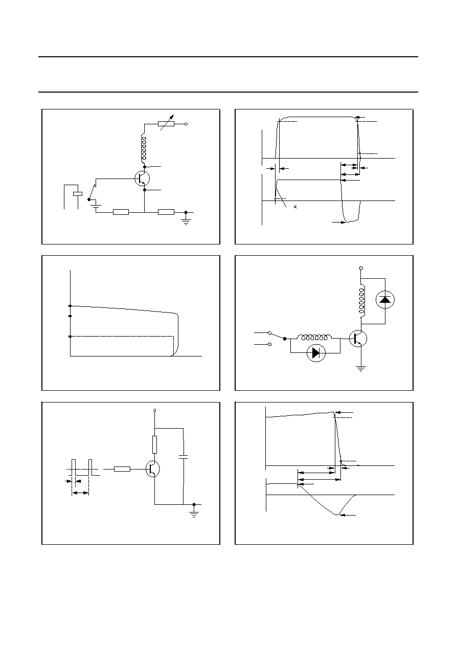
Fig.1. Test circuit for V
CEOsust
.
Fig.2. Oscilloscope display for V
CEOsust
.
Fig.3. Test circuit resistive load. V
IM
= -6 to +8 V
V
CC
= 250 V; t
p
= 20
�
s;
= t
p
/ T = 0.01.
R
B
and R
L
calculated from I
Con
and I
Bon
requirements.
Fig.4. Switching times waveforms with resistive load.
Fig.5. Test circuit inductive load.
V
CC
= 300 V; -V
BE
= 5 V; L
C
= 200 uH; L
B
= 1 uH
Fig.6. Switching times waveforms with inductive load.
+ 50v
100-200R
Horizontal
Vertical
Oscilloscope
1R
6V
30-60 Hz
300R
IC
IB
10 %
10 %
90 %
90 %
ton
toff
ts
tf
IBon
-IBoff
ICon
tr
30ns
VCE / V
min
VCEOsust
IC / mA
100
200
250
0
LB
IBon
-VBB
LC
T.U.T.
VCC
tp
T
VCC
R
R
T.U.T.
0
VIM
B
L
IC
IB
ICon
IBon
-IBoff
t
t
ts
tf
toff
10 %
90 %

August 1998
4
Rev 1.000
Philips Semiconductors
Product specification
Silicon Diffused Power Transistor
BUJ103A
Fig.7. Normalised power dissipation.
PD% = 100
PD/PD
25�C
= f (T
mb
)
Fig.8. Typical DC current gain. h
FE
= f(I
C
)
parameter V
CE
Fig.9. Collector-Emitter saturation voltage.
Solid lines = typ values, V
CEsat
= f(IB); T
j
=25�C.
Fig.10. Base-Emitter saturation voltage.
Solid lines = typ values, V
BEsat
= f(IC); at IC/IB =4.
Fig.11. Collector-Emitter saturation voltage.
Solid lines = typ values, V
CEsat
= f(IC); at IC/IB =4.
Fig.12. Transient thermal impedance.
Z
th j-mb
= f(t); parameter D = t
p
/T
0
20
40
60
80
100
120
140
Tmb / C
PD%
Normalised Power Derating
120
110
100
90
80
70
60
50
40
30
20
10
0
0.0
0.2
0.4
0.6
0.8
1.0
1.2
1.4
0.1
1
10
IC/A
VBEsat/V
0.01
1
100
10
1
0.1
10
h
FE
IC / A
Tj = 25 C
1V
5V
0.0
0.1
0.2
0.3
0.4
0.5
0.1
1
10
IC/A
VCEsat/V
0.0
0.4
0.8
1.2
1.6
2.0
0.01
0.10
1.00
10.00
IB/A
VCEsat/V
IC=1A
2A
3A
4A
1E-06
1E-04
1E-02
1E+00
t / s
Zth / (K/W)
10
1
0.1
0.01
0
0.5
0.2
0.1
0.05
0.02
D =
t p
T
T
P
t
D
t
p
D=