
Philips Semiconductors
Product specification
Logic level TOPFET
BUK128-50DL
SMD version of BUK117-50DL
DESCRIPTION
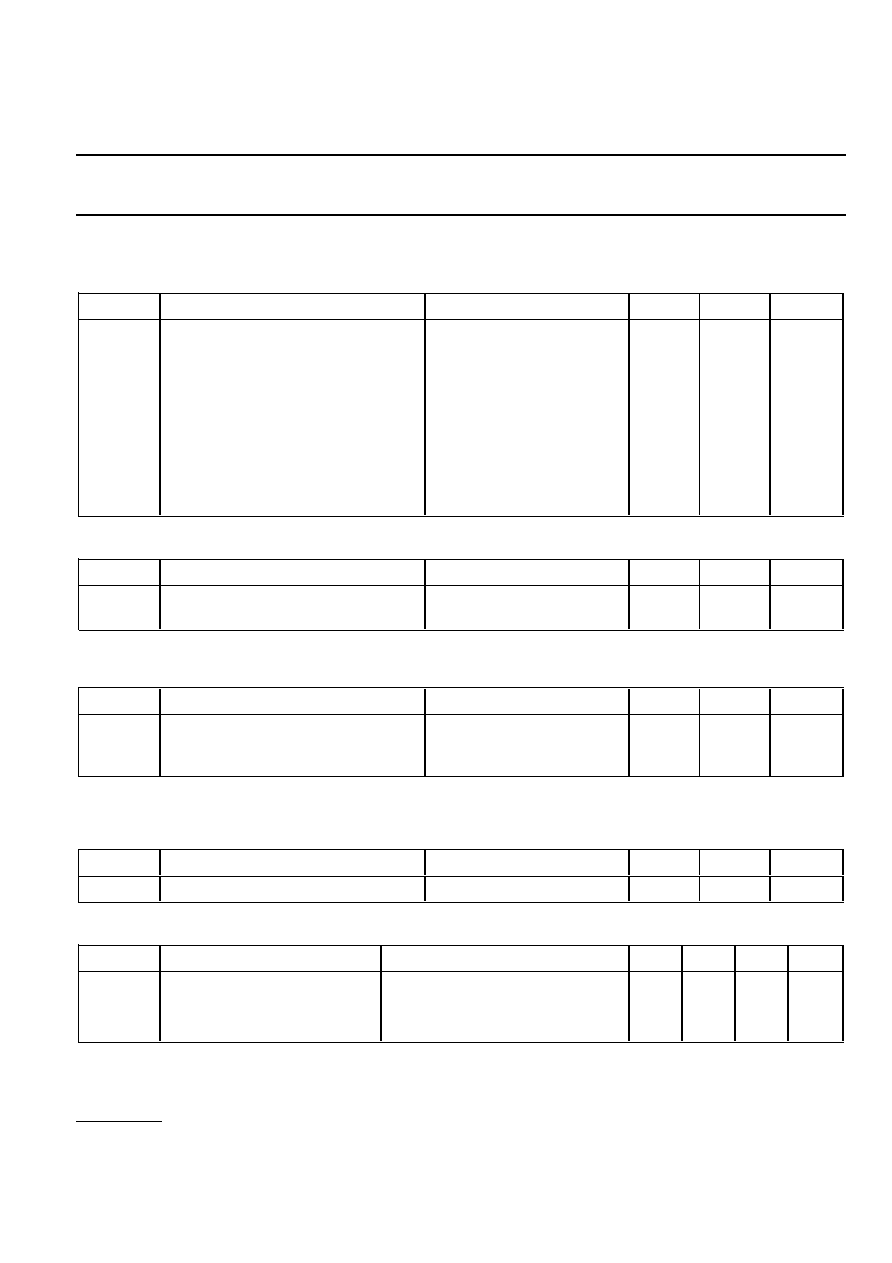
QUICK REFERENCE DATA
Monolithic temperature and
SYMBOL
PARAMETER
MAX.
UNIT
overload protected logic level power
MOSFET in TOPFET2 technology
V
DS
Continuous drain source voltage
50
V
assembled in a 3 pin surface mount
I
D
Continuous drain current
8
A
plastic package.
P
D
Total power dissipation
40
W
T
j
Continuous junction temperature
150
�C
APPLICATIONS
R
DS(ON)
Drain-source on-state resistance
100
m
General purpose switch for driving
I
ISL
Input supply current
V
IS
= 5 V
650
�
A
lamps
motors
solenoids
heaters
in automotive systems and other
applications.
FEATURES
FUNCTIONAL BLOCK DIAGRAM
TrenchMOS output stage
Current limiting
Overload protection
Overtemperature protection
Protection latched reset by input
5 V logic compatible input level
Control of output stage and
supply of overload protection
circuits derived from input
Low operating input current
permits direct drive by
micro-controller
ESD protection on all pins
Overvoltage clamping for turn
off of inductive loads
Fig.1. Elements of the TOPFET.
PINNING - SOT404
PIN CONFIGURATION
SYMBOL
PIN
DESCRIPTION
1
input
2
drain
3
source
mb
drain
DRAIN
SOURCE
INPUT
RIG
LOGIC AND
PROTECTION
O / V
CLAMP
POWER
MOSFET
1
3
mb
2
P
D
S
I
TOPFET
May 2001
1
Rev 1.800
Philips Semiconductors
Product specification
Logic level TOPFET
BUK128-50DL
SMD version of BUK117-50DL
LIMITING VALUES
Limiting values in accordance with the Absolute Maximum Rating System (IEC 134)
SYMBOL
PARAMETER
CONDITIONS
MIN.
MAX.
UNIT
V
DS
Continuous drain source voltage
1
-
-
50
V
I
D
Continuous drain current
V
IS
= 5 V; T
mb
=
25 �C
-
self -
A
limited
I
D
Continuous drain current
V
IS
= 5 V; T
mb
110 �C
-
8
A
I
I
Continuous input current
-
-5
5
mA
I
IRM
Non-repetitive peak input current
t
p
1 ms
-10
10
mA
P
D
Total power dissipation
T
mb
25 �C
-
40
W
T
stg
Storage temperature
-
-55
175
�C
T
j
Continuous junction temperature
2
normal operation
-
150
�C
T
sold
Case temperature
during soldering
-
260
�C
ESD LIMITING VALUE
SYMBOL
PARAMETER
CONDITIONS
MIN.
MAX.
UNIT
V
C
Electrostatic discharge capacitor
Human body model;
-
2
kV
voltage
C = 250 pF; R = 1.5 k
OVERVOLTAGE CLAMPING LIMITING VALUES
At a drain source voltage above 50 V the power MOSFET is actively turned on to clamp overvoltage transients.
SYMBOL
PARAMETER
CONDITIONS
MIN.
MAX.
UNIT
Inductive load turn-off
I
DM
= 8 A; V
DD
20 V
E
DSM
Non-repetitive clamping energy
T
mb
25 �C
-
100
mJ
E
DRM
Repetitive clamping energy
T
mb
95 �C; f = 250 Hz
-
20
mJ
OVERLOAD PROTECTION LIMITING VALUE
With an adequate protection supply provided via the input pin, TOPFET can protect itself from two types of overload
- overtemperature and short circuit load.
SYMBOL
PARAMETER
REQUIRED CONDITION
MIN.
MAX.
UNIT
V
DS
Drain source voltage
3
4 V
V
IS
5.5 V
0
35
V
THERMAL CHARACTERISTIC
SYMBOL
PARAMETER
CONDITIONS
MIN.
TYP.
MAX.
UNIT
Thermal resistance
R
th j-mb
Junction to mounting base
-
-
2.5
3.1
K/W
R
th j-a
Junction to ambient
minimum footprint FR4 PCB
-
50
-
K/W
1 Prior to the onset of overvoltage clamping. For voltages above this value, safe operation is limited by the overvoltage clamping energy.
2 A higher T
j
is allowed as an overload condition but at the threshold T
j(TO)
the over temperature trip operates to protect the switch.
3 All control logic and protection functions are disabled during conduction of the source drain diode.
May 2001
2
Rev 1.800

Philips Semiconductors
Product specification
Logic level TOPFET
BUK128-50DL
SMD version of BUK117-50DL
OUTPUT CHARACTERISTICS
Limits are for -40�C
T
mb
150�C; typicals are for T
mb
= 25 �C unless otherwise specified
SYMBOL
PARAMETER
CONDITIONS
MIN.
TYP.
MAX.
UNIT
Off-state
V
IS
= 0 V
V
(CL)DSS
Drain-source clamping voltage
I
D
= 10 mA
50
-
-
V
I
DM
= 1 A; t
p
300
�
s;
0.01
50
60
70
V
I
DSS
Drain source leakage current
V
DS
= 40 V
-
-
100
�
A
T
mb
= 25 �C
-
0.1
10
�
A
On-state
I
DM
= 3 A; t
p
300
�
s;
0.01
R
DS(ON)
Drain-source resistance
V
IS
4.4 V
-
-
190
m
T
mb
= 25 �C
-
68
100
m
V
IS
4 V
-
-
200
m
T
mb
= 25 �C
-
72
105
m
OVERLOAD CHARACTERISTICS
-40�C
T
mb
150�C unless otherwise specified.
SYMBOL
PARAMETER
CONDITIONS
MIN.
TYP.
MAX.
UNIT
Short circuit load
V
DS
= 13 V
I
D
Drain current limiting
V
IS
= 5 V;
T
mb
= 25�C
8
12
16
A
4.4 V
V
IS
5.5 V
6
-
18
A
4 V
V
IS
5.5 V
5
-
18
A
Overload protection
V
IS
= 5 V;
T
mb
= 25�C
P
D(TO)
Overload power threshold
device trips if P
D
> P
D(TO)
20
55
80
W
T
DSC
Characteristic time
which determines trip time
1
200
350
600
�
s
Overtemperature protection
T
j(TO)
Threshold junction
150
170
-
�C
temperature
2
1 Trip time t
d sc
varies with overload dissipation P
D
according to the formula t
d sc
T
DSC
/ ln[ P
D
/ P
D(TO)
].
2 This is independent of the dV/dt of input voltage V
IS
.
May 2001
3
Rev 1.800
Philips Semiconductors
Product specification
Logic level TOPFET
BUK128-50DL
SMD version of BUK117-50DL
INPUT CHARACTERISTICS
The supply for the logic and overload protection is taken from the input.
Limits are for -40�C
T
mb
150�C; typicals are for T
mb
= 25�C unless otherwise specified
SYMBOL
PARAMETER
CONDITIONS
MIN.
TYP.
MAX.
UNIT
V
IS(TO)
Input threshold voltage
V
DS
= 5 V; I
D
= 1 mA
0.6
-
2.4
V
T
mb
= 25�C
1.1
1.6
2.1
V
I
IS
Input supply current
normal operation;
V
IS
= 5 V
100
220
400
�
A
V
IS
= 4 V
80
195
330
�
A
I
ISL
Input supply current
protection latched;
V
IS
= 5 V
200
400
650
�
A
V
IS
= 3 V
130
250
430
�
A
V
ISR
Protection reset voltage
1
reset time t
r
100
�
s
1.5
2
2.9
V
t
lr
Latch reset time
V
IS1
= 5 V, V
IS2
< 1 V
10
40
100
�
s
V
(CL)IS
Input clamping voltage
I
I
= 1.5 mA
5.5
-
8.5
V
R
IG
Input series resistance
2
T
mb
= 25�C
-
33
-
k
to gate of power MOSFET
SWITCHING CHARACTERISTICS
T
mb
= 25 �C; V
DD
= 13 V; resistive load R
L
= 4
. Refer to waveform figure and test circuit.
SYMBOL
PARAMETER
CONDITIONS
MIN.
TYP.
MAX.
UNIT
t
d on
Turn-on delay time
V
IS
= 5 V
-
8
20
�
s
t
r
Rise time
-
20
50
�
s
t
d off
Turn-off delay time
V
IS
= 0 V
-
25
70
�
s
t
f
Fall time
-
16
40
�
s
1 The input voltage below which the overload protection circuits will be reset.
2 Not directly measureable from device terminals.
May 2001
4
Rev 1.800

Philips Semiconductors
Product specification
Logic level TOPFET
BUK128-50DL
SMD version of BUK117-50DL
MECHANICAL DATA
Fig.2. SOT404 surface mounting package
1
, centre pin connected to mounting base.
UNIT
A
REFERENCES
OUTLINE
VERSION
EUROPEAN
PROJECTION
ISSUE DATE
IEC
JEDEC
EIAJ
mm
A1
D1
D
max.
E
e
Lp
HD
Q
c
2.54
2.60
2.20
15.40
14.80
2.90
2.10
11
1.60
1.20
10.30
9.70
4.50
4.10
1.40
1.27
0.85
0.60
0.64
0.46
b
DIMENSIONS (mm are the original dimensions)
SOT404
0
2.5
5 mm
scale
Plastic single-ended surface mounted package (Philips version of D
2
-PAK); 3 leads
(one lead cropped)
SOT404
e
e
E
b
D1
HD
D
Q
Lp
c
A1
A
1
3
2
mounting
base
98-12-14
99-06-25
1 Epoxy meets UL94 V0 at 1/8". Net mass: 1.4 g
For soldering guidelines and SMD footprint design, please refer to Data Handbook SC18.
May 2001
5
Rev 1.800