Philips Semiconductors
Product specification
Silicon Diffused Power Transistor
BU2522AX
GENERAL DESCRIPTION
New generation, high-voltage, high-speed switching npn transistor in a plastic full-pack envelope intended for use in
horizontal deflection circuits of high resolution monitors. Features improved RBSOA performance and is suitable for
use in horizontal deflection circuits of pc monitors.
QUICK REFERENCE DATA
SYMBOL
PARAMETER
CONDITIONS
TYP.
MAX.
UNIT
V
CESM
Collector-emitter voltage peak value
V
BE
= 0 V
-
1500
V
V
CEO
Collector-emitter voltage (open base)
-
800
V
I
C
Collector current (DC)
-
10
A
I
CM
Collector current peak value
-
25
A
P
tot
Total power dissipation
T
hs
25 �C
-
45
W
V
CEsat
Collector-emitter saturation voltage
I
C
= 6.0 A; I
B
= 1.2 A
-
5.0
V
I
Csat
Collector saturation current
f = 64 kHz
6.0
-
A
t
f
Fall time
I
Csat
= 6.0 A; f = 64 kHz
0.16
0.22
�
s
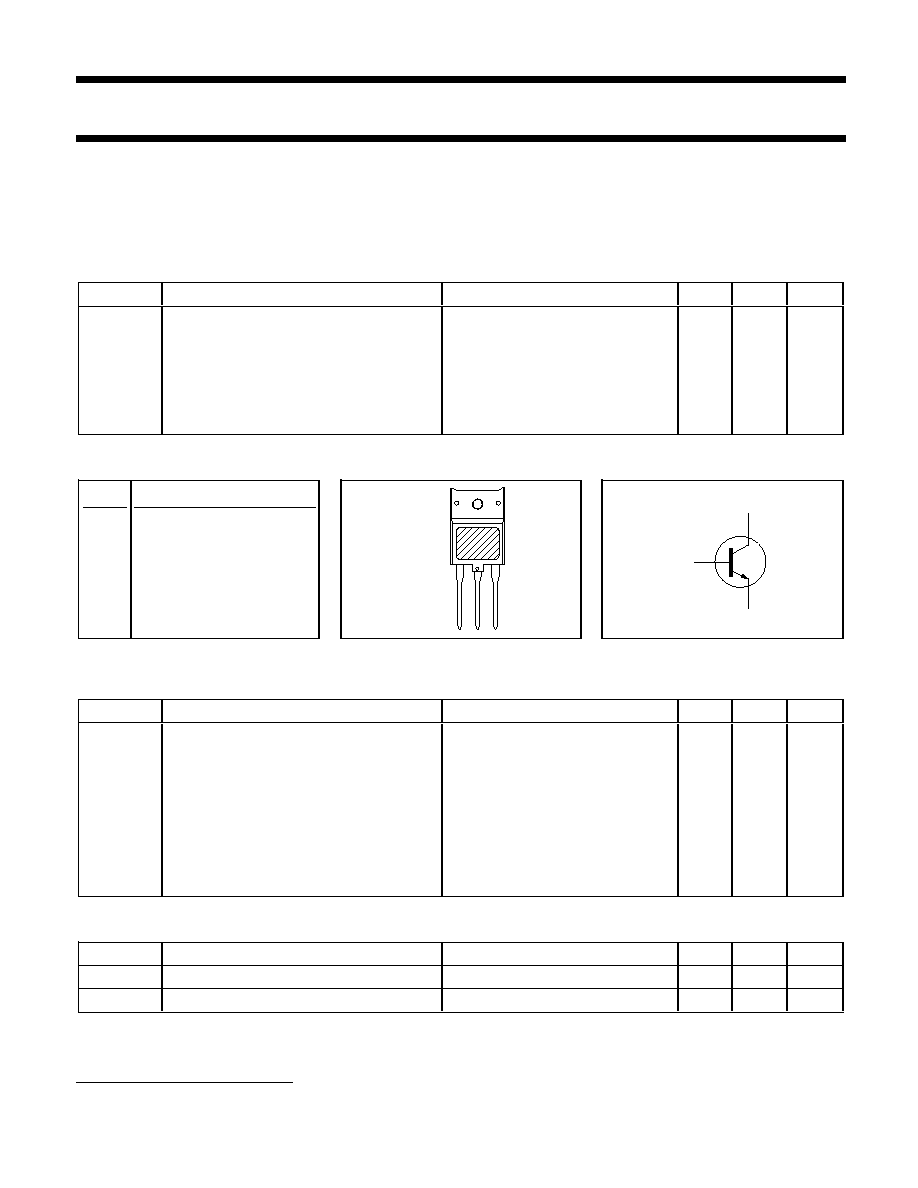
PINNING - SOT399
PIN CONFIGURATION
SYMBOL
PIN
DESCRIPTION
1
base
2
collector
3
emitter
case isolated
LIMITING VALUES
Limiting values in accordance with the Absolute Maximum Rating System (IEC 134)
SYMBOL
PARAMETER
CONDITIONS
MIN.
MAX.
UNIT
V
CESM
Collector-emitter voltage peak value
V
BE
= 0 V
-
1500
V
V
CEO
Collector-emitter voltage (open base)
-
800
V
I
C
Collector current (DC)
-
10
A
I
CM
Collector current peak value
-
25
A
I
B
Base current (DC)
-
6
A
I
BM
Base current peak value
-
9
A
-I
B(AV)
Reverse base current
average over any 20 ms period
-
150
mA
-I
BM
Reverse base current peak value
1
-
6
A
P
tot
Total power dissipation
T
hs
25 �C
-
45
W
T
stg
Storage temperature
-55
150
�C
T
j
Junction temperature
-
150
�C
THERMAL RESISTANCES
SYMBOL
PARAMETER
CONDITIONS
TYP.
MAX.
UNIT
R
th j-hs
Junction to heatsink
with heatsink compound
-
2.8
K/W
R
th j-a
Junction to ambient
in free air
35
-
K/W
case
1 2 3
b
c
e
1 Turn-off current.
September 1997
1
Rev 2.300

Philips Semiconductors
Product specification
Silicon Diffused Power Transistor
BU2522AX
ISOLATION LIMITING VALUE & CHARACTERISTIC
T
hs
= 25 �C unless otherwise specified
SYMBOL
PARAMETER
CONDITIONS
MIN.
TYP.
MAX.
UNIT
V
isol
Repetitive peak voltage from all
R.H.
65 % ; clean and dustfree
-
2500
V
three terminals to external
heatsink
C
isol
Capacitance from T2 to external f = 1 MHz
-
22
-
pF
heatsink
STATIC CHARACTERISTICS
T
hs
= 25 �C unless otherwise specified
SYMBOL
PARAMETER
CONDITIONS
MIN.
TYP.
MAX.
UNIT
I
CES
Collector cut-off current
2
V
BE
= 0 V; V
CE
= V
CESMmax
-
-
0.25
mA
I
CES
V
BE
= 0 V; V
CE
= V
CESMmax
;
-
-
2.0
mA
T
j
= 125 �C
I
EBO
Emitter cut-off current
V
EB
= 7.5 V; I
C
= 0 A
-
-
0.25
mA
BV
EBO
Emitter-base breakdown voltage
I
B
= 1 mA
7.5
13.5
-
V
V
CEOsust
Collector-emitter sustaining voltage
I
B
= 0 A; I
C
= 100 mA;
800
-
-
V
L = 25 mH
V
CEsat
Collector-emitter saturation voltage
I
C
= 6.0 A; I
B
= 1.2 A
-
-
5.0
V
V
BEsat
Base-emitter saturation voltage
I
C
= 6.0 A; I
B
= 1.2 A
-
-
1.3
V
h
FE
DC current gain
I
C
= 1 A; V
CE
= 5 V
-
10
-
h
FE
I
C
= 6 A; V
CE
= 5 V
5
7
8
DYNAMIC CHARACTERISTICS
T
hs
= 25 �C unless otherwise specified
SYMBOL
PARAMETER
CONDITIONS
TYP.
MAX.
UNIT
C
c
Collector capacitance
I
E
= 0 A; V
CB
= 10 V; f = 1 MHz
115
-
pF
Switching times (64 kHz line
I
Csat
= 6.0 A; L
C
= 170
�
H;
deflection circuit)
C
fb
= 5.4 nF;I
B(end)
= 0.7 A;
L
B
= 0.6
�
H; -V
BB
= 2 V;
(-dI
B
/dt= 3.33A /
�
s)
t
s
Turn-off storage time
1.7
2.0
�
s
t
f
Turn-off fall time
0.12
0.25
�
s
2 Measured with half sine-wave voltage (curve tracer).
September 1997
2
Rev 2.300
Philips Semiconductors
Product specification
Silicon Diffused Power Transistor
BU2522AX
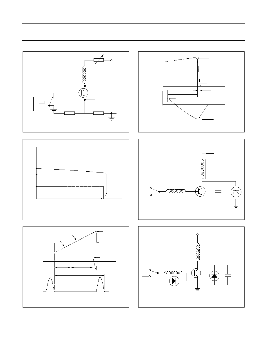
Fig.1. Test circuit for V
CEOsust
.
Fig.2. Oscilloscope display for V
CEOsust
.
Fig.3. Switching times waveforms (64 kHz).
Fig.4. Switching times definitions.
Fig.5. Switching times test circuit.
Fig.6. Test Circuit RBSOA. V
CC
= 140 V; -V
BB
= 4 V;
L
C
= 100 - 400
�
H; V
CL
1500 V; L
B
= 3
�
H;
C
FB
= 1 - 2.2 nF; I
B
(end) = 1.6 - 2 A
+ 50v
100-200R
Horizontal
Vertical
Oscilloscope
1R
6V
30-60 Hz
100R
ICsat
90 %
10 %
tf
ts
IBend
IC
IB
t
t
- IBM
VCE / V
min
VCEOsust
IC / mA
100
200
250
0
+ 150 v nominal
adjust for ICsat
Lc
Cfb
T.U.T.
LB
IBend
-VBB
V
ICsat
I end
16 us
6.5 us
5 us
t
t
t
TRANSISTOR
DIODE
B
I C
I B
CE
LB
IBend
-VBB
LC
T.U.T.
VCC
VCL
CFB
September 1997
3
Rev 2.300
Philips Semiconductors
Product specification
Silicon Diffused Power Transistor
BU2522AX
Fig.7. Typical DC current gain. h
FE
= f (I
C
)
V
CE
= 5 V
Fig.8. Typical base-emitter saturation voltage.
V
BE
sat = f (I
C
); parameter I
C
/I
B
Fig.9. Typical collector-emitter saturation voltage.
V
CE
sat = f (I
C
); parameter I
C
/I
B
Fig.10. Typical base-emitter saturation voltage.
V
BE
sat = f (I
B
); parameter I
C
Fig.11. Typical turn-off losses. T
j
= 85�C
Poff = f (I
B
); parameter I
C
= 6 A; f = 64 kHz
Fig.12. Typical collector storage and fall time.
ts = f (I
B
); tf = f (I
B
); parameter I
C
= 6A; T
j
= 85�C;
f = 64 kHz
0.01
0.1
1
10
100
IC / A
BU2522A
100
10
1
h
FE
Tj = 25 C
Tj = -40 C
Tj = 85 C
0
0.2 0.4 0.6 0.8
1
1.2 1.4 1.6 1.8
2
IB / A
1.2
1.1
1
0.9
0.8
0.7
0.6
BU2522A
VBESAT / V
Tj = 25 C
Tj = 85 C
IC =
7A
6A
5A
BU2522AF/DF/AX/DX
0
0.5
1
1.5
2
1
10
100
IB / A
PTOT / W
Ths = 25 C
Ths = 85 C
0.1
1
10
IC / A
1.2
1.1
1
0.9
0.8
0.7
0.6
0.5
0.4
VBESAT / V
BU2522A
Tj = 25 C
Tj = 85 C
IC/IB =
3
5
0
0.2
0.4
0.6
0.8
1
1.2
1.4
1.6
1.8
2
IB / A
ts, tf / us
BU2522AF
4
3.5
3
2.5
2
1.5
1
0.5
0
IC =
6A
5A
0.1
10
IC / A
VCESAT / V
10
1
0.1
0.01
100
1
BU2522A
Tj = 25 C
Tj = 85 C
IC/IB =
3
5
September 1997
4
Rev 2.300
Philips Semiconductors
Product specification
Silicon Diffused Power Transistor
BU2522AX
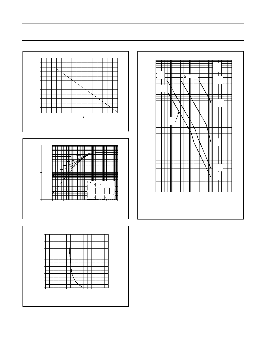
Fig.13. Normalised power dissipation.
PD% = 100
P
D
/P
D 25�C
= f (T
hs
)
Fig.14. Transient thermal impedance.
Z
th j-hs
= f(t); parameter D = t
p
/T
Fig.15. Reverse bias safe operating area. T
j
T
jmax
Fig.16. Forward bias safe operating area. T
hs
= 25 �C
I
CDC
& I
CM
= f(V
CE
); I
CM
single pulse; parameter t
p
Second-breakdown limits independant of temperature.
Mounted with heatsink compound.
0
20
40
60
80
100
120
140
Ths / C
PD%
Normalised Power Derating
120
110
100
90
80
70
60
50
40
30
20
10
0
with heatsink compound
BU2520AF
IC / A
100
10
1
0.1
0.01
1
10
100
1000
VCE / V
100 us
1 ms
10 ms
DC
30 us
tp =
Ptot
ICM
ICDC
= 0.01
1E-06
1E-04
1E-02
1E+00
t / s
Zth / (K/W)
D = 0
0.02
0.05
0.1
0.2
0.5
D =
t
p
t
p
T
T
P
t
D
10
1
0.1
0.01
0.001
BU2522AF
0
30
20
10
0
500
1000
1500
VCE / V
IC / A
September 1997
5
Rev 2.300