Äîêóìåíòàöèÿ è îïèñàíèÿ www.docs.chipfind.ru
BUK71/7907-55AIE
TrenchPLUS standard level FET
Rev. 01 -- 12 August 2002
Product data
1.
Product profile
1.1 Description
N-channel enhancement mode field-effect power transistor in a plastic package using
TrenchMOSTM technology, featuring very low on-state resistance, TrenchPLUS
current sensing and diodes for ESD protection.
Product availability:
BUK7107-55AIE in SOT426 (D
2
-PAK)
BUK7907-55AIE in SOT263B (TO-220AB).
1.2 Features
1.3 Applications
1.4 Quick reference data
2.
Pinning information
s
Integrated current sensor
s
Q101 compliant
s
ESD protection
s
Standard level compatible.
s
Variable Valve Timing for engines
s
Electrical Power Assisted Steering.
s
V
DS
55 V
s
R
DSon
= 5.8 m
(typ)
s
I
D
140 A
s
I
D
/I
sense
= 500 (typ).
Table 1:
Pinning - SOT426 and SOT263B, simplified outline and symbol
Pin
Description
Simplified outline
Symbol
1
gate (g)
SOT426 (D
2
-PAK)
SOT263B (TO-220AB)
2
I
sense
3
drain (d)
4
Kelvin source
5
source (s)
mb
mounting base;
connected to drain (d)
Front view
MBK127
1 2
4
3
5
mb
1
5
mb
MBL263
MBL368
d
s
Isense
Kelvin source
g

Philips Semiconductors
BUK71/7907-55AIE
TrenchPLUS standard level FET
Product data
Rev. 01 -- 12 August 2002
2 of 15
9397 750 09877
© Koninklijke Philips Electronics N.V. 2002. All rights reserved.
3.
Limiting values
[1]
Current is limited by power dissipation chip rating
[2]
Continuous current is limited by package.
Table 2:
Limiting values
In accordance with the Absolute Maximum Rating System (IEC 60134).
Symbol
Parameter
Conditions
Min
Max
Unit
V
DS
drain-source voltage (DC)
-
55
V
V
DGS
drain-gate voltage (DC)
I
DG
= 250
µ
A
-
55
V
V
GS
gate-source voltage (DC)
-
±
20
V
I
D
drain current (DC)
T
mb
= 25
°
C; V
GS
= 10 V;
Figure 2
and
3
[1]
-
140
A
[2]
-
75
A
T
mb
= 100
°
C; V
GS
= 10 V;
Figure 2
[2]
-
75
A
I
DM
peak drain current
T
mb
= 25
°
C; pulsed; t
p
10
µ
s;
Figure 3
-
560
A
P
tot
total power dissipation
T
mb
= 25
°
C;
Figure 1
-
272
W
I
GS(CL)
gate-source clamping current
continuous
-
10
mA
t
p
= 5 ms;
= 0.01
-
50
mA
T
stg
storage temperature
-
55
+175
°
C
T
j
junction temperature
-
55
+175
°
C
Source-drain diode
I
DR
reverse drain current
T
mb
= 25
°
C
[1]
-
140
A
[2]
-
75
A
I
DRM
peak reverse drain current
T
mb
= 25
°
C; pulsed; t
p
10
µ
s
-
560
A
Avalanche ruggedness
E
DS(AL)S
non-repetitive drain-source avalanche
energy
unclamped inductive load; I
D
= 68 A;
V
DS
55 V; V
GS
= 10 V; R
GS
= 50
;
starting T
j
= 25
°
C
-
460
mJ
Electrostatic Discharge
V
esd
electrostatic discharge voltage; all pins Human Body Model; C = 100 pF;
R = 1.5 k
6
kV
Philips Semiconductors
BUK71/7907-55AIE
TrenchPLUS standard level FET
Product data
Rev. 01 -- 12 August 2002
3 of 15
9397 750 09877
© Koninklijke Philips Electronics N.V. 2002. All rights reserved.
V
GS
10 V
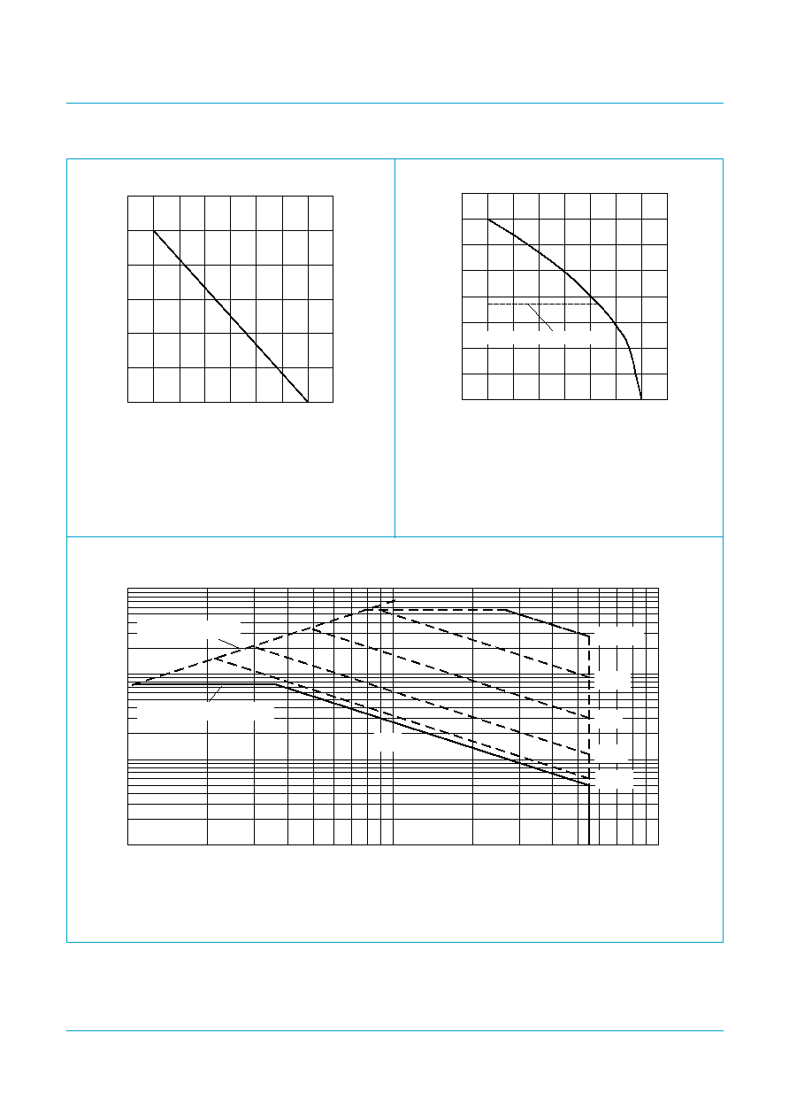
Fig 1.
Normalized total power dissipation as a
function of mounting base temperature.
Fig 2.
Continuous drain current as a function of
mounting base temperature.
T
mb
= 25
°
C; I
DM
single pulse.
Fig 3.
Safe operating area; continuous and peak drain currents as a function of drain-source voltage.
03na19
0
40
80
120
0
50
100
150
200
Tmb
(°
C)
Pder
(%)
03ni63
0
40
80
120
160
0
50
100
150
200
Capped at 75A due to package
Tmb (
°
C)
ID
(A)
P
der
P
tot
P
tot 25 C
°
(
)
-----------------------
100%
×
=
03nf55
1
10
102
103
1
10
102
VDS (V)
ID
(A)
DC
100 ms
10 ms
Limit RDSon = VDS/ID
1 ms
tp = 10
µ
s
100
µ
s
Capped at 75 A due to package
Philips Semiconductors
BUK71/7907-55AIE
TrenchPLUS standard level FET
Product data
Rev. 01 -- 12 August 2002
4 of 15
9397 750 09877
© Koninklijke Philips Electronics N.V. 2002. All rights reserved.
4.
Thermal characteristics
4.1 Transient thermal impedance
Table 3:
Thermal characteristics
Symbol
Parameter
Conditions
Min
Typ
Max Unit
R
th(j-a)
thermal resistance from junction to ambient
SOT263B
vertical in still air
-
60
-
K/W
SOT426
minimum footprint; mounted on a PCB
-
50
-
K/W
R
th(j-mb)
thermal resistance from junction to
mounting base
Figure 4
-
-
0.55 K/W
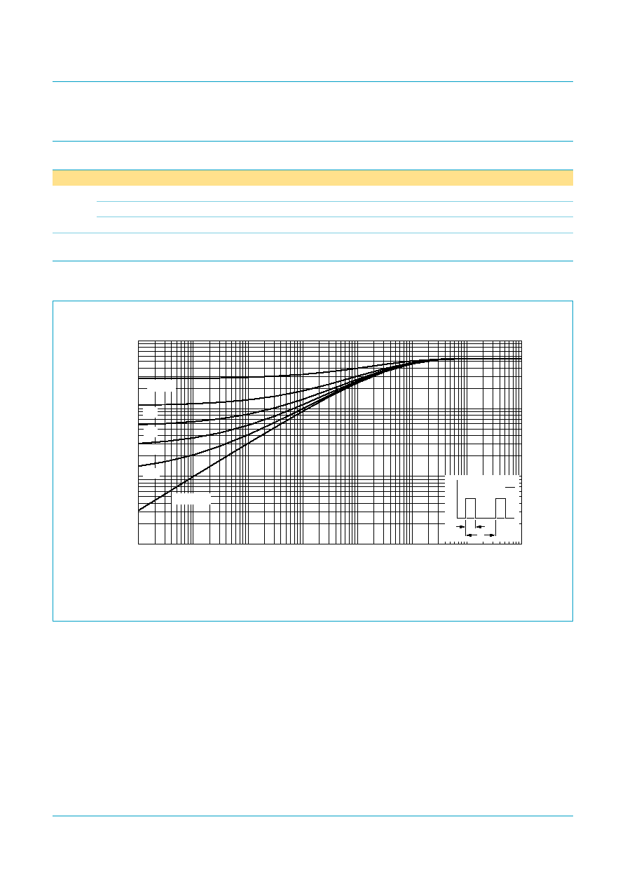
Fig 4.
Transient thermal impedance from junction to mounting base as a function of pulse duration.
03ni29
single shot
0.2
0.1
0.05
0.02
10-3
10-2
10-1
1
10-6
10-5
10-4
10-3
10-2
10-1
1
10
tp (s)
Z th(j-mb)
(K/W)
= 0.5
tp
tp
T
P
t
T
=

Philips Semiconductors
BUK71/7907-55AIE
TrenchPLUS standard level FET
Product data
Rev. 01 -- 12 August 2002
5 of 15
9397 750 09877
© Koninklijke Philips Electronics N.V. 2002. All rights reserved.
5.
Characteristics
Table 4:
Characteristics
T
j
= 25
°
C unless otherwise specified.
Symbol
Parameter
Conditions
Min
Typ
Max
Unit
Static characteristics
V
(BR)DSS
drain-source breakdown
voltage
I
D
= 0.25 mA; V
GS
= 0 V
T
j
= 25
°
C
55
-
-
V
T
j
=
-
55
°
C
50
-
-
V
V
GS(th)
gate-source threshold voltage I
D
= 1 mA; V
DS
= V
GS
;
Figure 9
T
j
= 25
°
C
2
3
4
V
T
j
= 175
°
C
1
-
-
V
T
j
=
-
55
°
C
-
-
4.4
V
I
DSS
drain-source leakage current
V
DS
= 55 V; V
GS
= 0 V
T
j
= 25
°
C
-
0.1
10
µ
A
T
j
= 175
°
C
-
-
250
µ
A
V
(BR)GSS
gate-source breakdown
voltage
I
G
=
±
1 mA;
-
55
°
C < T
j
<175
°
C
20
22
-
V
I
GSS
gate-source leakage current
V
GS
=
±
10 V; V
DS
= 0 V
T
j
= 25
°
C
-
22
1000
nA
T
j
= 175
°
C
-
-
10
µ
A
R
DSon
drain-source on-state
resistance
V
GS
= 10 V; I
D
= 50 A;
Figure 7
and
8
T
j
= 25
°
C
-
5.8
7
m
T
j
= 175
°
C
-
-
14
m
I
D
/I
sense
ratio of drain current to sense
current
V
GS
> 10 V;
-
55
°
C < T
j
<175
°
C
450
500
550
Dynamic characteristics
Q
g(tot)
total gate charge
V
GS
= 10 V; V
DS
= 44 V;
I
D
= 25 A;
Figure 14
-
116
-
nC
Q
gs
gate-source charge
-
19
-
nC
Q
gd
gate-to-drain (Miller) charge
-
50
-
nC
C
iss
input capacitance
V
GS
= 0 V; V
DS
= 25 V;
f = 1 MHz;
Figure 12
-
4500
-
pF
C
oss
output capacitance
-
960
-
pF
C
rss
reverse transfer capacitance
-
510
-
pF
t
d(on)
turn-on delay time
V
DS
= 30 V; R
L
= 1.2
;
V
GS
= 10 V; R
G
= 10
-
36
-
ns
t
r
rise time
-
115
-
ns
t
d(off)
turn-off delay time
-
159
-
ns
t
f
fall time
-
111
-
ns
L
d
internal drain inductance
from upper edge of drain
mounting base to center of
die
-
2.5
-
nH
L
s
internal source inductance
from source lead to source
bond pad
-
7.5
-
nH
Document Outline