Äîêóìåíòàöèÿ è îïèñàíèÿ www.docs.chipfind.ru
Philips Semiconductors
Product specification
TrenchMOS
transistor
BUK9528-100A
Logic level FET
BUK9628-100A
GENERAL DESCRIPTION
QUICK REFERENCE DATA
N-channel enhancement mode logic
SYMBOL
PARAMETER
MAX.
UNIT
level field-effect power transistor in a
plastic
envelope
available
in
V
DS
Drain-source voltage
100
V
TO220AB and SOT404 . Using
I
D
Drain current (DC)
49
A
'trench' technology which features
P
tot
Total power dissipation
166
W
very low on-state resistance. It is
T
j
Junction temperature
175
°C
intended for use in automotive and
R
DS(ON)
Drain-source on-state
general
purpose
switching
resistance
V
GS
= 5 V
28
m
applications.
V
GS
= 10 V
27
m
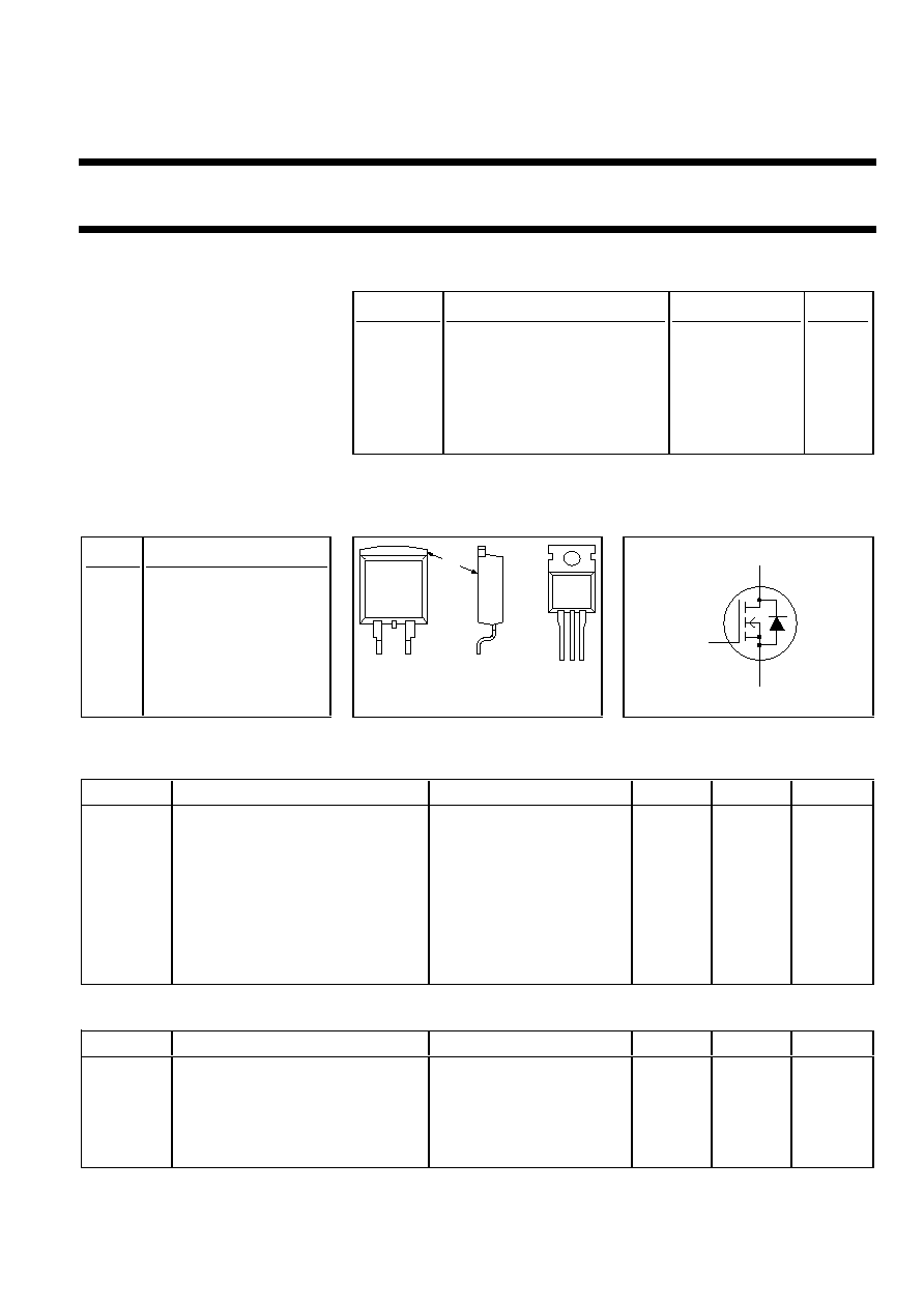
PINNING
TO220AB & SOT404
PIN CONFIGURATION
SYMBOL
PIN
DESCRIPTION
1
gate
2
drain
3
source
tab/mb drain
LIMITING VALUES
Limiting values in accordance with the Absolute Maximum System (IEC 134)
SYMBOL
PARAMETER
CONDITIONS
MIN.
MAX.
UNIT
V
DS
Drain-source voltage
-
-
100
V
V
DGR
Drain-gate voltage
R
GS
= 20 k
-
100
V
±
V
GS
Gate-source voltage
-
-
10
V
±
V
GSM
Non-repetitive gate-source voltage
t
p
50
µ
S
-
15
V
I
D
Drain current (DC)
T
mb
= 25 °C
-
49
A
I
D
Drain current (DC)
T
mb
= 100 °C
-
34
A
I
DM
Drain current (pulse peak value)
T
mb
= 25 °C
-
195
A
P
tot
Total power dissipation
T
mb
= 25 °C
-
166
W
T
stg
, T
j
Storage & operating temperature
-
- 55
175
°C
THERMAL RESISTANCES
SYMBOL
PARAMETER
CONDITIONS
TYP.
MAX.
UNIT
R
th j-mb
Thermal resistance junction to
-
-
0.9
K/W
mounting base
R
th j-a
Thermal resistance junction to
in free air
60
-
K/W
ambient(TO220AB)
R
th j-a
Thermal resistance junction to
Minimum footprint, FR4
50
-
K/W
ambient(SOT404)
board
1 2 3
tab
1
3
mb
2
SOT404
TO220AB
d
g
s
March 2000
1
Rev 1.000

Philips Semiconductors
Product specification
TrenchMOS
transistor
BUK9528-100A
Logic level FET
BUK9628-100A
STATIC CHARACTERISTICS
T
j
= 25°C unless otherwise specified
SYMBOL
PARAMETER
CONDITIONS
MIN.
TYP.
MAX.
UNIT
V
(BR)DSS
Drain-source breakdown
V
GS
= 0 V; I
D
= 0.25 mA;
100
-
-
V
voltage
T
j
= -55°C
89
-
-
V
V
GS(TO)
Gate threshold voltage
V
DS
= V
GS
; I
D
= 1 mA
1
1.5
2.0
V
T
j
= 175°C
0.5
-
-
V
T
j
= -55°C
-
-
2.3
V
I
DSS
Zero gate voltage drain current
V
DS
= 100 V; V
GS
= 0 V;
-
0.05
10
µ
A
T
j
= 175°C
-
-
500
µ
A
I
GSS
Gate source leakage current
V
GS
=
±
10 V; V
DS
= 0 V
-
2
100
nA
R
DS(ON)
Drain-source on-state
V
GS
= 5 V; I
D
= 25 A
-
18.5
28
m
resistance
T
j
= 175°C
-
-
70
m
V
GS
= 10 V; I
D
= 25 A
-
17
27
m
V
GS
= 4.5 V; I
D
= 25 A
-
18.8
31
m
DYNAMIC CHARACTERISTICS
T
mb
= 25°C unless otherwise specified
SYMBOL
PARAMETER
CONDITIONS
MIN.
TYP.
MAX.
UNIT
C
iss
Input capacitance
V
GS
= 0 V; V
DS
= 25 V; f = 1 MHz
-
3220
4293
pF
C
oss
Output capacitance
-
315
378
pF
C
rss
Feedback capacitance
-
187
256
pF
t
d on
Turn-on delay time
V
DD
= 30 V; R
load
=1.2
;
-
11
16
ns
t
r
Turn-on rise time
V
GS
= 5 V; R
G
= 10
-
58
87
ns
t
d off
Turn-off delay time
-
250
350
ns
t
f
Turn-off fall time
-
106
148
ns
L
d
Internal drain inductance
Measured from drain lead 6 mm
-
4.5
-
nH
from package to centre of die
L
d
Internal drain inductance
Measured from contact screw on
-
3.5
-
nH
tab to centre of die(TO220AB)
L
d
Internal drain inductance
Measured from upper edge of drain
-
2.5
-
nH
tab to centre of die(SOT404)
L
s
Internal source inductance
Measured from source lead to
-
7.5
-
nH
source bond pad
REVERSE DIODE LIMITING VALUES AND CHARACTERISTICS
T
j
= 25°C unless otherwise specified
SYMBOL
PARAMETER
CONDITIONS
MIN.
TYP.
MAX.
UNIT
I
DR
Continuous reverse drain
-
-
49
A
current
I
DRM
Pulsed reverse drain current
-
-
195
A
V
SD
Diode forward voltage
I
F
= 25 A; V
GS
= 0 V
-
0.85
1.2
V
I
F
= 49 A; V
GS
= 0 V
-
1.1
-
V
t
rr
Reverse recovery time
I
F
= 49 A; -dI
F
/dt = 100 A/
µ
s;
-
63
-
ns
Q
rr
Reverse recovery charge
V
GS
= -10 V; V
R
= 30 V
-
0.22
-
µ
C
March 2000
2
Rev 1.000
Philips Semiconductors
Product specification
TrenchMOS
transistor
BUK9528-100A
Logic level FET
BUK9628-100A
AVALANCHE LIMITING VALUE
SYMBOL
PARAMETER
CONDITIONS
MIN.
TYP.
MAX.
UNIT
W
DSS
1
Drain-source non-repetitive
I
D
= 30 A; V
DD
25 V;
-
-
45
mJ
unclamped inductive turn-off
V
GS
= 5 V; R
GS
= 50
; T
mb
= 25 °C
energy
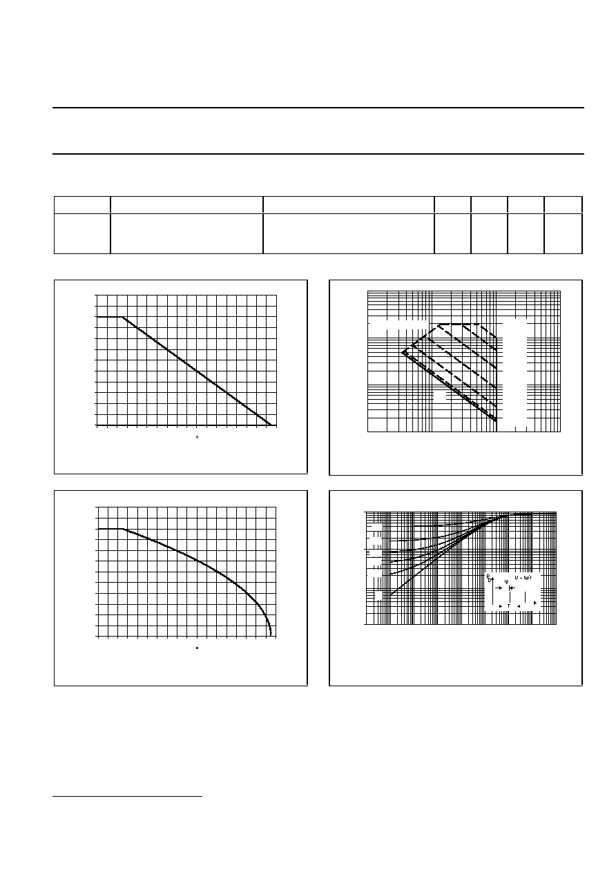
Fig.1. Normalised power dissipation.
PD% = 100
P
D
/P
D 25 °C
= f(T
mb
)
Fig.2. Normalised continuous drain current.
ID% = 100
I
D
/I
D 25 °C
= f(T
mb
); conditions: V
GS
5 V
Fig.3. Safe operating area. T
mb
= 25 °C
I
D
& I
DM
= f(V
DS
); I
DM
single pulse; parameter t
p
Fig.4. Transient thermal impedance.
Z
th j-mb
= f(t); parameter D = t
p
/T
0
20
40
60
80
100
120
140
160
180
Tmb / C
PD%
Normalised Power Derating
120
110
100
90
80
70
60
50
40
30
20
10
0
1
10
100
1000
1
10
100
1000
tp =
1us
10us
100us
1ms
10ms
100ms
DC
RDS(ON)=VDS/ID
VSD/V
ID/A
0
20
40
60
80
100
120
140
160
180
Tmb / C
ID%
Normalised Current Derating
120
110
100
90
80
70
60
50
40
30
20
10
0
0.001
0.01
0.1
1
1E-07
1E-05
1E-03
1E-01
1E+01
t/s
Zth/(K/W)
0
0.02
0.05
0.1
0.2
0.5
1 For maximum permissible repetive avalanche current see fig.18.
March 2000
3
Rev 1.000
Philips Semiconductors
Product specification
TrenchMOS
transistor
BUK9528-100A
Logic level FET
BUK9628-100A
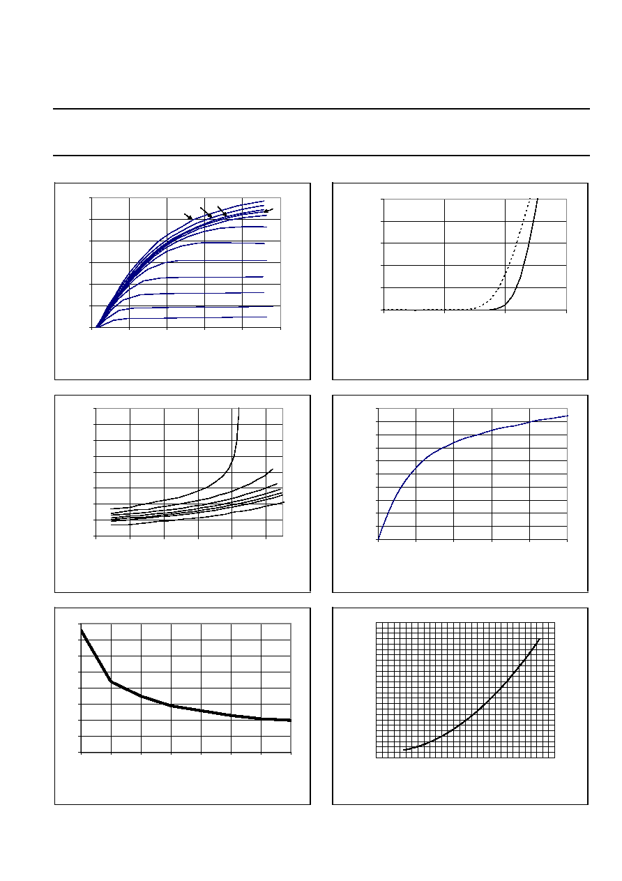
Fig.5. Typical output characteristics, T
j
= 25 °C.
I
D
= f(V
DS
); parameter V
GS
Fig.6. Typical on-state resistance, T
j
= 25 °C.
R
DS(ON)
= f(I
D
); paramter V
GS
Fig.7. Typical on-state resistance, T
j
= 25 °C.
R
DS(ON)
= f(V
GS
); conditions: I
D
= 25 A;
Fig.8. Typical transfer characteristics.
I
D
= f(V
GS
) ; conditions: V
DS
= 25 V; parameter T
j
Fig.9. Typical transconductance, T
j
= 25 °C.
g
fs
= f(I
D
); conditions: V
DS
= 25 V
Fig.10. Normalised drain-source on-state resistance.
a = R
DS(ON)
/R
DS(ON)25 °C
= f(T
j
); I
D
= 25 A; V
GS
= 5 V
0
10
20
30
40
50
60
0
2
4
6
8
10
VDS/V
ID/A
2.8
3.0
3.6
3.8
4.0
5.0
10.0
VGS/V =
2.2
2.6
3.4
3.2
2.4
0
5
10
15
20
25
0.0
2.0
4.0
6.0
VGS/V
ID/A
Tj/C= 175
25
25
30
35
40
45
50
55
60
65
5
15
25
35
45
55
ID/A
RDS(ON)/mOhm
3.2
3.6
3.8
3.0
3.4
5.0
4.0
0
10
20
30
40
50
60
70
80
90
100
0
20
40
60
80
100
ID/A
gfs/S
15
16
17
18
19
20
21
22
23
3
4
5
6
7
8
9
10
VGS/V
RDS(ON) Ohm
0.5
1
1.5
2
2.5
3
-100
-50
0
50
100
150
200
Tmb / degC
a
Rds(on) normalised to 25degC
March 2000
4
Rev 1.000
Philips Semiconductors
Product specification
TrenchMOS
transistor
BUK9528-100A
Logic level FET
BUK9628-100A
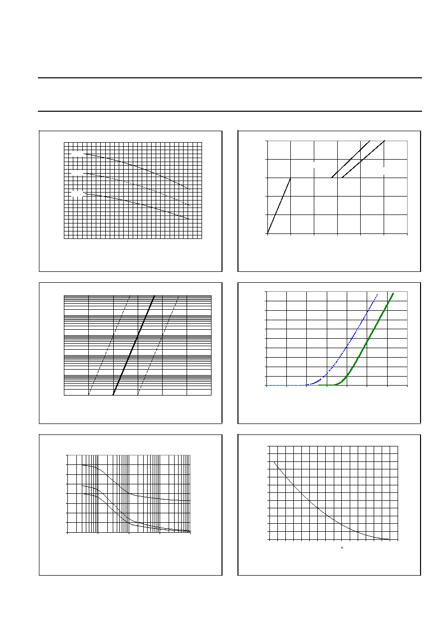
Fig.11. Gate threshold voltage.
V
GS(TO)
= f(T
j
); conditions: I
D
= 1 mA; V
DS
= V
GS
Fig.12. Sub-threshold drain current.
I
D
= f(V
GS)
; conditions: T
j
= 25 °C; V
DS
= V
GS
Fig.13. Typical capacitances, C
iss
, C
oss
, C
rss
.
C = f(V
DS
); conditions: V
GS
= 0 V; f = 1 MHz
Fig.14. Typical turn-on gate-charge characteristics.
V
GS
= f(Q
G
); conditions: I
D
= 25 A; parameter V
DS
Fig.15. Typical reverse diode current.
I
F
= f(V
SDS
); conditions: V
GS
= 0 V; parameter T
j
Fig.16. Normalised avalanche energy rating.
W
DSS
% = f(T
mb
); conditions: I
D
= 75 A
-100
-50
0
50
100
150
200
0
0.5
1
1.5
2
2.5
Tj / C
VGS(TO) / V
max.
typ.
min.
0
1
2
3
4
5
0
10
20
30
40
50
60
QG / nC
VGS / V
VDS = 14V
VDS = 44V
0
0.5
1
1.5
2
2.5
3
1E-05
1E-05
1E-04
1E-03
1E-02
1E-01
Sub-Threshold Conduction
2%
typ
98%
0
10
20
30
40
50
60
70
80
90
100
0.0
0.2
0.4
0.6
0.8
1.0
1.2
1.4
VSDS/V
IF/A
25
o
C
Tj/C= 175
o
C
0.0
1.0
2.0
3.0
4.0
5.0
6.0
7.0
8.0
0.01
0.1
1
10
100
VDS/V
C
a
pa
c
i
t
a
nc
e
/
pF
Ciss
Coss
Crss
20
40
60
80
100
120
140
160
180
Tmb / C
120
110
100
90
80
70
60
50
40
30
20
10
0
WDSS%
March 2000
5
Rev 1.000
Document Outline