Äîêóìåíòàöèÿ è îïèñàíèÿ www.docs.chipfind.ru

BUK98180-100A
TrenchMOSTM logic level FET
Rev. 02 -- 18 May 2001
Product data
c
c
1.
Description
N-channel enhancement mode field-effect power transistor in a plastic package using
TrenchMOSTM
1
technology, featuring very low on-state resistance.
Product availability:
BUK98180-100A in SOT223 (SC-73).
2.
Features
s
TrenchMOSTM technology
s
Q101 compliant
s
150
°
C rated
s
Logic level compatible.
3.
Applications
s
Automotive and general purpose power switching
x
12 V, 24 V and 42 V loads
x
Motors, lamps and solenoids.
4.
Pinning information
1.
TrenchMOS is a trademark of Royal Philips Electronics.
Table 1:
Pinning - SOT223 (SC-73), simplified outline and symbol
Pin
Description
Simplified outline
Symbol
1
gate (g)
SOT223 (SC-73)
2
drain (d)
3
source (s)
4
drain (d)
4
1
2
3
MSB002 - 1
Top view
s
d
g
MBB076

Philips Semiconductors
BUK98180-100A
TrenchMOSTM logic level FET
Product data
Rev. 02 -- 18 May 2001
2 of 13
9397 750 08277
© Philips Electronics N.V. 2001. All rights reserved.
5.
Quick reference data
6.
Limiting values
Table 2:
Quick reference data
Symbol Parameter
Conditions
Typ
Max
Unit
V
DS
drain-source voltage (DC)
-
100
V
I
D
drain current (DC)
T
sp
= 25
°
C; V
GS
= 5 V
-
4.6
A
P
tot
total power dissipation
T
sp
= 25
°
C
-
8
W
T
j
junction temperature
-
150
°
C
R
DSon
drain-source on-state resistance
T
j
= 25
°
C; V
GS
= 5 V; I
D
= 5 A
153
180
m
T
j
= 25
°
C; V
GS
= 4.5 V; I
D
= 5 A
-
201
m
T
j
= 25
°
C; V
GS
= 10 V; I
D
= 5 A
147
173
m
Table 3:
Limiting values
In accordance with the Absolute Maximum Rating System (IEC 60134).
Symbol Parameter
Conditions
Min
Max
Unit
V
DS
drain-source voltage (DC)
-
100
V
V
DGR
drain-gate voltage (DC)
R
GS
= 20 k
-
100
V
V
GS
gate-source voltage (DC)
-
±
10
V
V
GSM
non-repetitive gate-source voltage
t
p
50
µ
s
-
±
15
V
I
D
drain current (DC)
T
sp
= 25
°
C; V
GS
= 5 V;
Figure 2
and
3
-
4.6
A
T
sp
= 100
°
C; V
GS
= 5 V;
Figure 2
-
3
A
I
DM
peak drain current
T
sp
= 25
°
C; pulsed; t
p
10
µ
s;
Figure 3
-
18
A
P
tot
total power dissipation
T
sp
= 25
°
C;
Figure 1
-
8
W
T
stg
storage temperature
-
55
+150
°
C
T
j
operating junction temperature
-
55
+150
°
C
Source-drain diode
I
DR
reverse drain current (DC)
T
sp
= 25
°
C
-
4.6
A
I
DRM
pulsed reverse drain current
T
sp
= 25
°
C; pulsed; t
p
10
µ
s
-
18
A
Avalanche ruggedness
W
DSS
non-repetitive avalanche energy
unclamped inductive load; I
D
= 4 A;
V
DS
100 V; V
GS
= 5 V; R
GS
= 50
;
starting T
sp
= 25
°
C
-
16
mJ
Philips Semiconductors
BUK98180-100A
TrenchMOSTM logic level FET
Product data
Rev. 02 -- 18 May 2001
3 of 13
9397 750 08277
© Philips Electronics N.V. 2001. All rights reserved.
V
GS
4.5 V
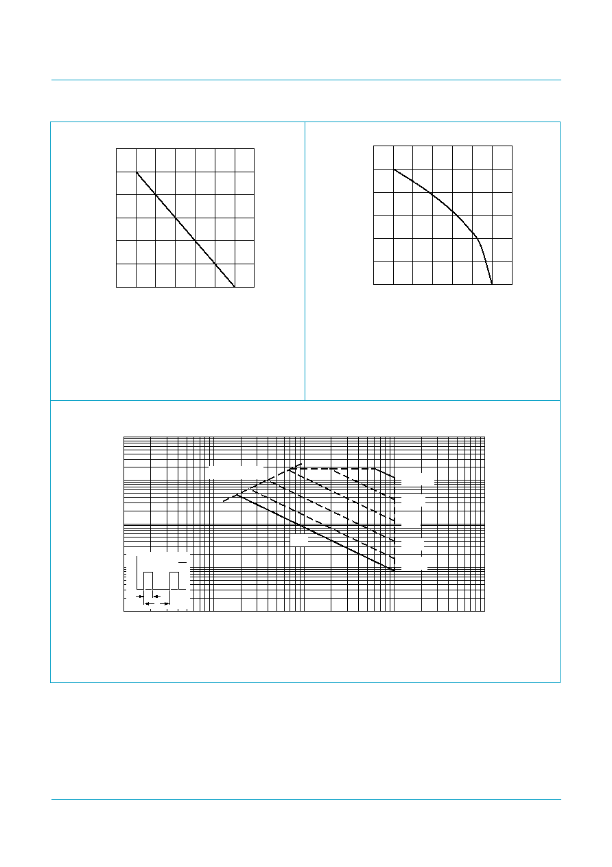
Fig 1.
Normalized total power dissipation as a
function of solder point temperature.
Fig 2.
Normalized continuous drain current as a
function of solder point temperature.
T
amb
= 25
°
C; I
DM
is single pulse.
Fig 3.
Safe operating area; continuous and peak drain currents as a function of drain-source voltage.
03aa17
0
20
40
60
80
100
120
0
25
50
75
100
125
150
175
P
der
Tsp (
o
C)
(%)
03aa25
0
20
40
60
80
100
120
0
25
50
75
100
125
150
175
I
der
T
sp
(
o
C)
(%)
P
der
P
tot
P
tot 25 C
°
(
)
----------------------
100%
×
=
I
der
I
D
I
D 25 C
°
(
)
-------------------
100%
×
=
03nc34
10-2
10-1
1
10
102
10-1
1
10
102
103
VDS (V)
ID
(A)
D.C.
100 ms
10 ms
RDSon = VDS / ID
1 ms
tp = 10 us
100 us
tp
tp
T
P
t
T
=
Philips Semiconductors
BUK98180-100A
TrenchMOSTM logic level FET
Product data
Rev. 02 -- 18 May 2001
4 of 13
9397 750 08277
© Philips Electronics N.V. 2001. All rights reserved.
7.
Thermal characteristics
7.1 Transient thermal impedance
Table 4:
Thermal characteristics
Symbol
Parameter
Conditions
Value
Unit
R
th(j-a)
thermal resistance from junction to ambient
70
K/W
R
th(j-sp)
thermal resistance from junction to solder
point
Figure 4
15
K/W
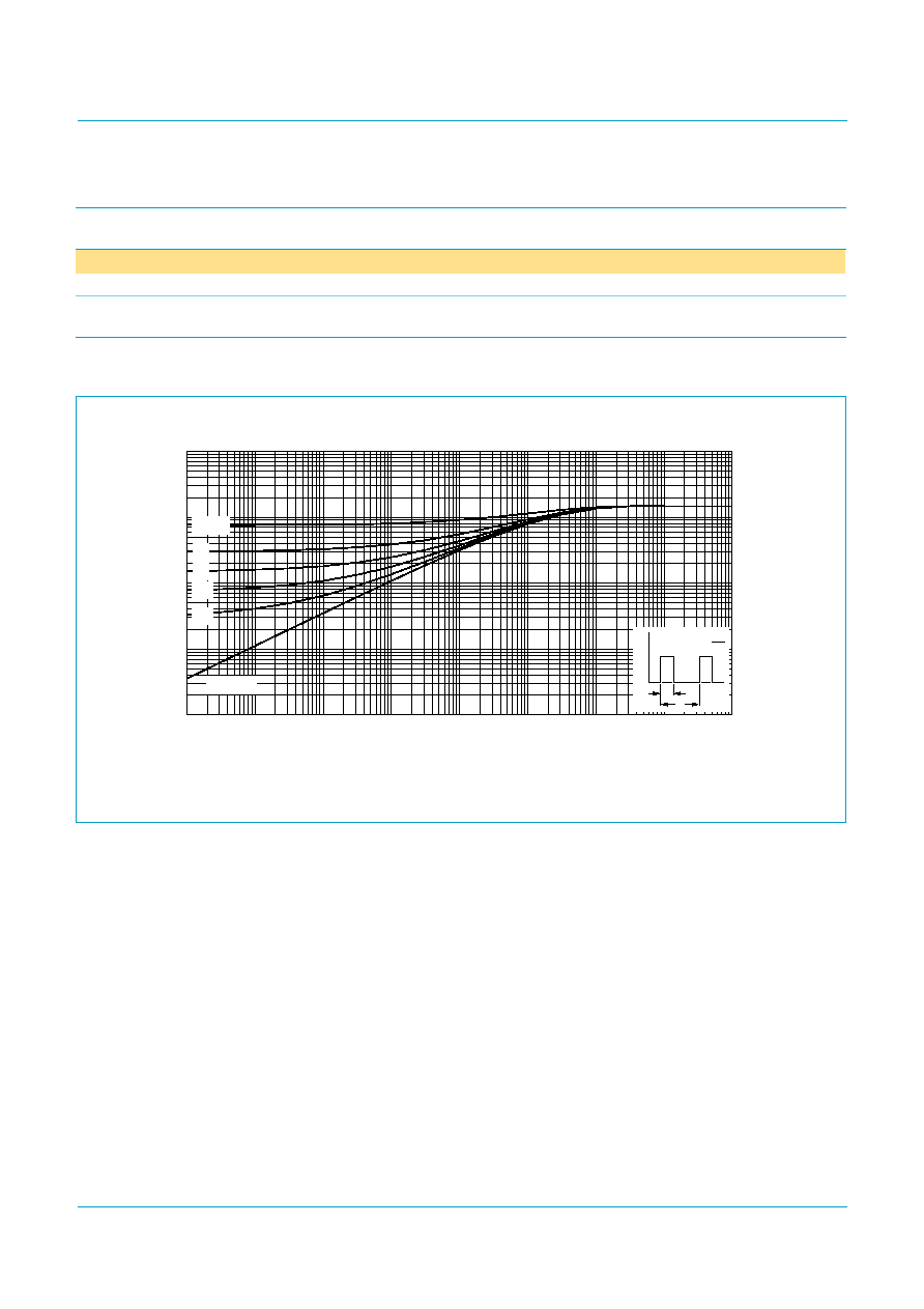
Fig 4.
Transient thermal impedance from junction to solder point as a function of pulse duration.
03nc35
Single Shot
0.2
0.1
0.05
0.02
10-2
10-1
1
10
102
10-6
10-5
10-4
10-3
10-2
10-1
1
10
102
tp (s)
Zth(j-sp)
(K/W)
= 0.5
tp
tp
T
P
t
T
=

Philips Semiconductors
BUK98180-100A
TrenchMOSTM logic level FET
Product data
Rev. 02 -- 18 May 2001
5 of 13
9397 750 08277
© Philips Electronics N.V. 2001. All rights reserved.
8.
Characteristics
Table 5:
Characteristics
T
j
= 25
°
C unless otherwise specified
Symbol
Parameter
Conditions
Min
Typ
Max
Unit
Static characteristics
V
(BR)DSS
drain-source breakdown
voltage
I
D
= 0.25 mA; V
GS
= 0 V
T
j
= 25
°
C
100
-
-
V
T
j
=
-
55
°
C
89
-
-
V
V
GS(th)
gate-source threshold voltage I
D
= 1 mA; V
DS
= V
GS
;
Figure 9
T
j
= 25
°
C
1
1.5
2
V
T
j
= 150
°
C
0.6
-
-
V
T
j
=
-
55
°
C
-
-
2.3
V
I
DSS
drain-source leakage current
V
DS
= 100 V; V
GS
= 0 V
T
j
= 25
°
C
-
0.05
10
µ
A
T
j
= 150
°
C
-
-
500
µ
A
I
GSS
gate-source leakage current
V
GS
=
±
10 V; V
DS
= 0 V
-
2
100
nA
R
DSon
drain-source on-state
resistance
V
GS
= 5 V; I
D
= 5 A;
Figure 7
and
8
T
j
= 25
°
C
-
153
180
m
T
j
= 150
°
C
-
-
389
m
V
GS
= 4.5 V; I
D
= 5 A;
-
-
201
m
V
GS
= 10 V; I
D
= 5 A;
-
147
173
m
Dynamic characteristics
C
iss
input capacitance
V
GS
= 0 V; V
DS
= 25 V;
f = 1 MHz;
Figure 12
-
464
619
pF
C
oss
output capacitance
-
60
72
pF
C
rss
reverse transfer capacitance
-
36
50
pF
t
d(on)
turn-on delay time
V
DD
= 30 V; R
L
= 1.2
;
V
GS
= 5 V; R
G
= 10
-
7
-
ns
t
r
rise time
-
89
-
ns
t
d(off)
turn-off delay time
-
18
-
ns
t
f
fall time
-
25
-
ns
Document Outline