 | –≠–ª–µ–∫—Ç—Ä–æ–Ω–Ω—ã–π –∫–æ–º–ø–æ–Ω–µ–Ω—Ç: BUT11 | –°–∫–∞—á–∞—Ç—å:  PDF PDF  ZIP ZIP |

DATA SHEET
Product specification
Supersedes data of February 1996
File under Discrete Semiconductors, SC06
1997 Aug 13
DISCRETE SEMICONDUCTORS
BUT11; BUT11A
Silicon diffused power transistors

1997 Aug 13
1
Philips Semiconductors
Product specification
Silicon diffused power transistors
BUT11; BUT11A
DESCRIPTION
High-voltage, high-speed,
glass-passivated NPN power
transistor in a TO-220AB package.
APPLICATIONS
∑
Converters
∑
Inverters
∑
Switching regulators
∑
Motor control systems.
PINNING
PIN
DESCRIPTION
1
base
2
collector; connected to
mounting base
3
emitter
andbook, halfpage
MBK106
1 2 3
Fig.1 Simplified outline (TO-220AB) and symbol.
handbook, halfpage
3
2
1
MBB008
QUICK REFERENCE DATA
SYMBOL
PARAMETER
CONDITIONS
MAX.
UNIT
V
CESM
collector-emitter peak voltage
V
BE
= 0
BUT11
850
V
BUT11A
1000
V
V
CEO
collector-emitter voltage
open base
BUT11
400
V
BUT11A
450
V
V
CEsat
collector-emitter saturation voltage
see Figs 7 and 9
1.5
V
I
C
collector current (DC)
see Figs 2 and 4
5
A
I
CM
collector current (peak value)
see Fig. 4
10
A
P
tot
total power dissipation
T
mb
25
∞
C; see Fig.3
100
W
t
f
fall time
resistive load; see Figs 11 and 12
0.8
µ
s
THERMAL CHARACTERISTICS
SYMBOL
PARAMETER
VALUE
UNIT
R
th j-mb
thermal resistance from junction to mounting base
1.25
K/W
1997 Aug 13
2
Philips Semiconductors
Product specification
Silicon diffused power transistors
BUT11; BUT11A
LIMITING VALUES
In accordance with the Absolute Maximum Rating System (IEC 134).
SYMBOL
PARAMETER
CONDITIONS
MIN.
MAX.
UNIT
V
CESM
collector-emitter peak voltage
V
BE
= 0
BUT11
-
850
V
BUT11A
-
1000
V
V
CEO
collector-emitter voltage
open base
BUT11
-
400
V
BUT11A
-
450
V
I
C
collector current (DC)
see Figs 2 and 4
-
5
A
I
CM
collector current (peak value)
t
p
< 2 ms; see Fig. 4
-
10
A
I
B
base current (DC)
-
2
A
I
BM
base current (peak value)
t
p
< 2 ms
-
4
A
P
tot
total power dissipation
T
mb
25
∞
C; see Fig.3
-
100
W
T
stg
storage temperature
-
65
+150
∞
C
T
j
junction temperature
-
150
∞
C
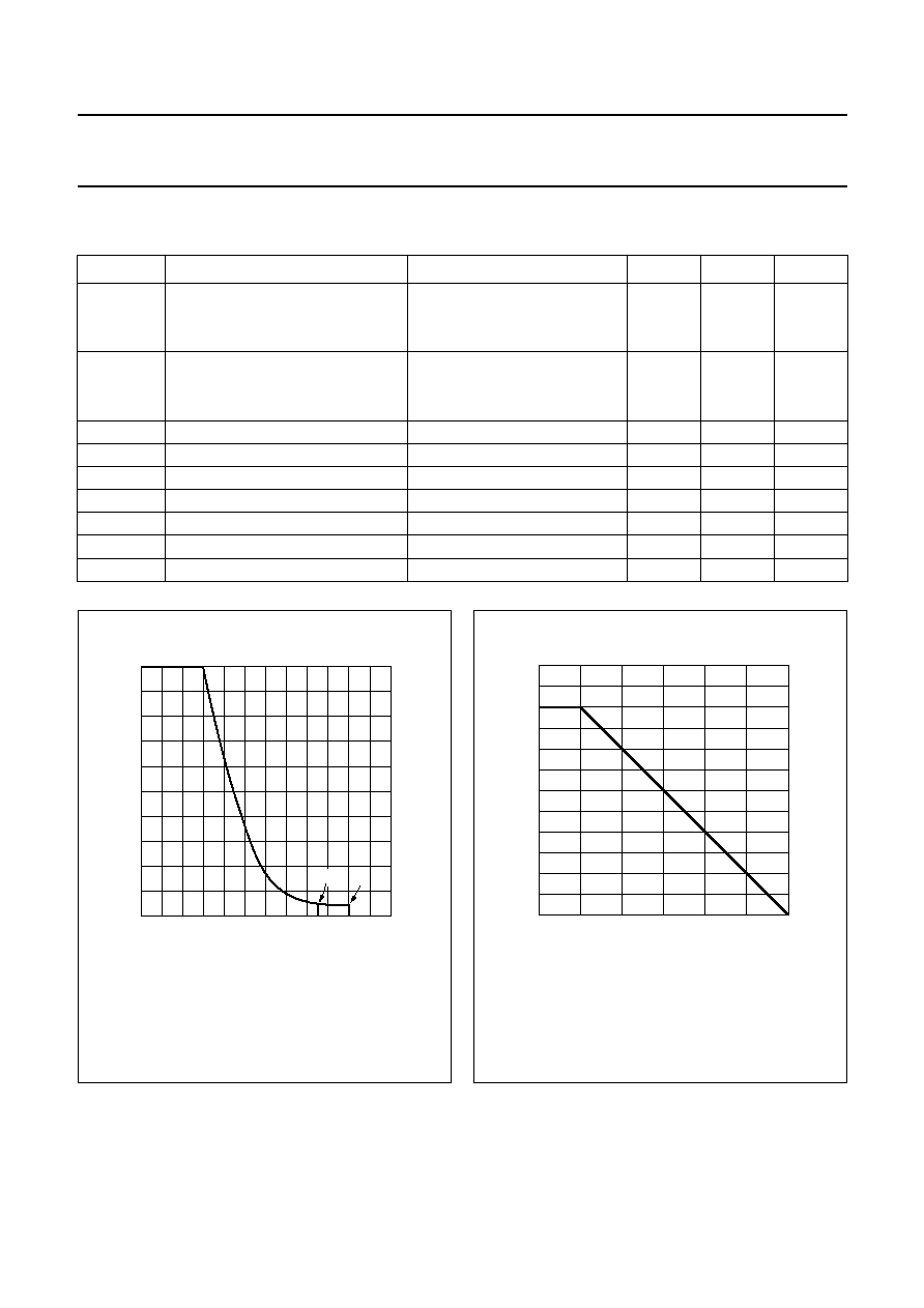
Fig.2 Reverse bias SOAR.
handbook, halfpage
0
400
IC
(A)
1200
VCE (V)
0
MGB895
800
(2)
1
2
3
4
5
(1)
(1) BUT11.
(2) BUT11A.
Fig.3 Power derating curve.
handbook, halfpage
0
50
Tmb (
o
C)
100
150
120
0
40
80
MGD283
Ptot max
(%)

1997 Aug 13
3
Philips Semiconductors
Product specification
Silicon diffused power transistors
BUT11; BUT11A
CHARACTERISTICS
T
j
= 25
∞
C unless otherwise specified.
Note
1. Measured with a half-sinewave voltage (curve tracer).
SYMBOL
PARAMETER
CONDITIONS
MIN.
TYP.
MAX. UNIT
V
CEOsust
collector-emitter sustaining voltage I
C
= 100 mA; I
Boff
= 0; L = 25 mH; see
Figs 5 and 6
BUT11
400
-
-
V
BUT11A
450
-
-
V
V
CEsat
collector-emitter saturation voltage
BUT11
I
C
= 3 A; I
B
= 600 mA; see Figs 7 and 9
-
-
1.5
V
BUT11A
I
C
= 2.5 A; I
B
= 500 mA; see
Figs 7 and 9
-
-
1.5
V
V
BEsat
base-emitter saturation voltage
BUT11
I
C
= 3 A; I
B
= 0.6 A; see Fig.7
-
-
1.3
V
BUT11A
I
C
= 2.5 A; I
B
= 0.5 A; see Fig.7
-
-
1.3
V
I
CES
collector-emitter cut-off current
V
CE
= V
CESMmax
; V
BE
= 0; note 1
-
-
1
mA
V
CE
= V
CESMmax
; V
BE
= 0; T
j
= 125
∞
C;
note 1
-
-
2
mA
I
EBO
emitter-base cut-off current
V
EB
= 9 V; I
C
= 0
-
-
10
mA
h
FE
DC current gain
V
CE
= 5 V; I
C
= 5 mA; see Fig.10
10
18
35
V
CE
= 5 V; I
C
= 500 mA; see Fig.10
10
20
35
Switching times resistive load (see Fig.12)
t
on
turn-on time
BUT11
I
Con
= 3 A; I
Bon
=
-
I
Boff
= 600 mA
-
-
1
µ
s
BUT11A
I
Con
= 2.5 A; I
Bon
=
-
I
Boff
= 500 mA
-
-
1
µ
s
t
s
storage time
BUT11
I
Con
= 3 A; I
Bon
=
-
I
Boff
= 600 mA
-
-
4
µ
s
BUT11A
I
Con
= 2.5 A; I
Bon
=
-
I
Boff
= 500 mA
-
-
4
µ
s
t
f
fall time
BUT11
I
Con
= 3 A; I
Bon
=
-
I
Boff
= 600 mA
-
-
0.8
µ
s
BUT11A
I
Con
= 2.5 A; I
Bon
=
-
I
Boff
= 500 mA
-
-
0.8
µ
s
Switching times inductive load (see Fig.14)
t
s
storage time
BUT11
I
Con
= 3 A; I
Bon
= 600 mA
-
1.1
1.4
µ
s
I
Con
= 3 A; I
Bon
= 600 mA; T
j
= 100
∞
C
-
1.2
1.5
µ
s
BUT11A
I
Con
= 2.5 A; I
Bon
= 500 mA
-
1.1
1.4
µ
s
I
Con
= 2.5 A; I
Bon
= 500 mA; T
j
= 100
∞
C
-
1.2
1.5
µ
s
t
f
fall time
BUT11
I
Con
= 3 A; I
Bon
= 600 mA
-
80
150
ns
I
Con
= 3 A; I
Bon
= 600 mA; T
j
= 100
∞
C
-
140
300
ns
BUT11A
I
Con
= 2.5 A; I
Bon
= 500 mA
-
80
150
ns
I
Con
= 2.5 A; I
Bon
= 500 mA; T
j
= 100
∞
C
-
140
300
ns

1997 Aug 13
4
Philips Semiconductors
Product specification
Silicon diffused power transistors
BUT11; BUT11A
Fig.4 Forward bias SOAR.
T
mb
25
∞
C.
I - Region of permissible DC operation.
II - Permissible extension for repetitive pulse operation.
III - Area of permissible operation during turn-on in single transistor converters, provided R
BE
100
and t
p
0.6
µ
s.
IV - Repetitive pulse operation in this region is permissible provided V
BE
0 and t
p
5 ms.
(1) P
tot max
and P
tot peak max
lines.
(2) Second breakdown limits.
handbook, full pagewidth
MGB950
1
10
10
2
10
3
10
4
VCE (V)
10
10
-
1
10
-
2
10
2
10
-
3
IC
(A)
(1)
(2)
I
II
III
IV
IC max
BUT11
BUT11A
1 ms
2 ms
10 ms
DC
200
µ
s
500
µ
s
tp =
20
µ
s
100
µ
s
50
µ
s
= 0.01
ICM max