 | ÐлекÑÑоннÑй компоненÑ: BYC8B-600 | СкаÑаÑÑ:  PDF PDF  ZIP ZIP |
Äîêóìåíòàöèÿ è îïèñàíèÿ www.docs.chipfind.ru
Philips Semiconductors
Product specification
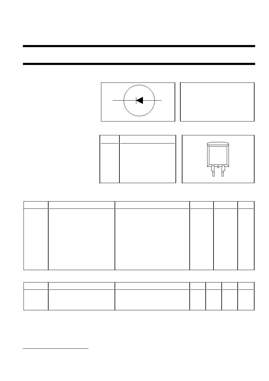
Rectifier diode
BYC8B-600
ultrafast, low switching loss
FEATURES
SYMBOL
QUICK REFERENCE DATA
· Extremely fast switching
V
R
= 600 V
· Low reverse recovery current
· Low thermal resistance
V
F
1.85 V
· Reduces switching losses in
associated MOSFET
I
F(AV)
= 8 A
t
rr
= 19 ns (typ)
APPLICATIONS
PINNING
SOT404
· Active power factor correction
PIN
DESCRIPTION
· Half-bridge lighting ballasts
· Half-bridge/ full-bridge switched
1
no connection
mode power supplies.
2
cathode
1
The BYC8B-600 is supplied in the
SOT404 surface mounting
3
anode
package.
tab
cathode
LIMITING VALUES
Limiting values in accordance with the Absolute Maximum System (IEC 134).
SYMBOL
PARAMETER
CONDITIONS
MIN.
MAX.
UNIT
V
RRM
Peak repetitive reverse voltage
-
600
V
V
RWM
Crest working reverse voltage
-
600
V
V
R
Continuous reverse voltage
T
mb
110 °C
-
500
V
I
F(AV)
Average forward current
= 0.5; with reapplied V
RRM(max)
;
-
8
A
T
mb
82 °C
1
I
FRM
Repetitive peak forward current
= 0.5; with reapplied V
RRM(max)
;
-
16
A
T
mb
82 °C
1
I
FSM
Non-repetitive peak forward
t = 10 ms
-
55
A
current.
t = 8.3 ms
-
60
A
sinusoidal; T
j
= 150°C prior to surge
with reapplied V
RWM(max)
T
stg
Storage temperature
-40
150
°C
T
j
Operating junction temperature
-
150
°C
THERMAL RESISTANCES
SYMBOL
PARAMETER
CONDITIONS
MIN.
TYP.
MAX.
UNIT
R
th j-mb
Thermal resistance junction to
-
-
2.2
K/W
mounting base
R
th j-a
Thermal resistance junction to
minimum footprint, FR4 board
-
50
-
K/W
ambient
k
a
tab
3
1
3
tab
2
1 it is not possible to make connection to pin 2 of the SOT404 package
October 1998
1
Rev 1.200
Philips Semiconductors
Product specification
Rectifier diode
BYC8B-600
ultrafast, low switching loss
ELECTRICAL CHARACTERISTICS
T
j
= 25 °C unless otherwise stated
SYMBOL
PARAMETER
CONDITIONS
MIN.
TYP.
MAX.
UNIT
V
F
Forward voltage
I
F
= 8 A; T
j
= 150°C
-
1.4
1.85
V
I
F
= 16 A; T
j
= 150°C
-
1.7
2.3
V
I
F
= 8 A;
-
2.0
2.8
V
I
R
Reverse current
V
R
= 600 V
-
9
150
µ
A
V
R
= 500 V; T
j
= 100 °C
-
1.1
3.0
mA
t
rr
Reverse recovery time
I
F
= 8 A to V
R
= 400 V;
-
19
-
ns
dI
F
/dt = 500 A/
µ
s
t
rr
Reverse recovery time
I
F
= 8 A to V
R
= 400 V;
-
32
40
ns
dI
F
/dt = 500 A/
µ
s; T
j
= 125°C
I
rrm
Peak reverse recovery current
I
F
= 8 A to V
R
= 400 V;
-
9.5
12
A
dI
F
/dt = 500 A/
µ
s; T
j
= 125°C
V
fr
Forward recovery voltage
I
F
= 10 A; dI
F
/dt = 100 A/
µ
s
-
8
10
V
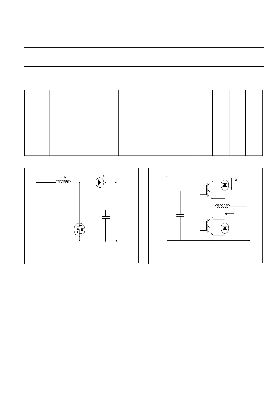
Fig.1. Typical application, output rectifier in boost
converter power factor correction circuit. Continuous
conduction, mode where the transistor turns on whilst
forward current is still flowing in the diode.
Fig.2. Typical application, freewheeling diode in half
bridge converter. Continuous conduction mode, where
each transistor turns on whilst forward current is still
flowing in the other bridge leg diode.
Vin
Vo = 400 V d.c.
500 V MOSFET
IL
150 uH
ID
OUTPUT DIODE
typ
Vin
Vin = 400 V d.c.
inductive load
IF
IR
IL
October 1998
2
Rev 1.200
Philips Semiconductors
Product specification
Rectifier diode
BYC8B-600
ultrafast, low switching loss
Fig.3. Maximum forward dissipation as a function of
average forward current; rectangular current
waveform where I
F(AV)
=I
F(RMS)
x
D.
Fig.4. Typical reverse recovery switching losses in
diode, as a function of rate of change of current dI
F
/dt.
Fig.5. Typical switching losses in transistor due to
reverse recovery of diode, as a function of of change
of current dI
F
/dt.
Fig.6. Origin of switching losses in transistor due to
diode reverse recovery.
Fig.7. Typical reverse recovery time t
rr
, as a function
of rate of change of current dI
F
/dt.
Fig.8. Typical peak reverse recovery current, I
rrm
as a
function of rate of change of current dI
F
/dt.
0
2
4
6
8
10
12
0
5
10
15
20
25
D = 1.0
0.5
0.2
0.1
BYC8-600
Rs = 0.05625 Ohms
Vo = 1.4 V
150
Average forward current, IF(AV) (A)
Forward dissipation, PF (W)
Tmb(max) C
139
128
117
106
95
D =
t
p
t
p
T
T
t
I
time
ID
Irrm
VD
dIF/dt
ID = IL
losses due to
diode reverse recovery
100
1000
0
0.05
0.1
0.15
0.2
0.25
BYC8-600
Rate of change of current, dIF/dt (A/us)
f = 20 kHz
Diode reverse recovery switching losses, Pdsw (W)
IF = 8 A
Tj = 125 C
VR = 400 V
16 A
12 A
100
1000
10
100
BYC8-600
Rate of change of current, dIF/dt (A/us)
Reverse recovery time, trr (ns)
IF = 5 A
16 A
12 A
8 A
Tj = 125 C
VR = 400 V
100
1000
0
1
2
3
4
5
6
7
8
BYC8-600
Rate of change of current, dIF/dt (A/us)
Transistor losses due to diode reverse recovery, Ptsw (W)
IF = 5 A
12 A
16 A
8 A
f = 20 kHz
Tj = 125 C
VR = 400 V
100
1000
1
10
100
BYC8-600
Rate of change of current, dIF/dt (A/us)
Peak reverse recovery current, Irrm (A)
Tj = 125 C
VR = 400 V
IF = 5 A
16 A
October 1998
3
Rev 1.200
Philips Semiconductors
Product specification
Rectifier diode
BYC8B-600
ultrafast, low switching loss
Fig.9. Definition of reverse recovery parameters t
rr
, I
rrm
Fig.10. Typical forward recovery voltage, V
fr
as a
function of rate of change of current dI
F
/dt.
Fig.11. Definition of forward recovery voltage V
fr
Fig.12. Typical and maximum forward characteristic
I
F
= f(V
F
); T
j
= 25°C and 150°C.
Fig.13. Typical reverse leakage current as a function
of reverse voltage. I
R
= f(V
R
); parameter T
j
Fig.14. Maximum thermal impedance Z
th j-mb
as a
function of pulse width.
Q
s
100%
10%
time
dI
dt
F
I
R
I
F
I
rrm
t
rr
0
1
2
3
4
0
5
10
15
20
BYC8-600
Forward voltage, VF (V)
Forward current, IF (A)
max
typ
Tj = 25 C
Tj = 150 C
0
50
100
150
200
0
5
10
15
20
BYC8-600
Tj = 25 C
Rate of change of current, dIF/dt (A/ s)
Peak forward recovery voltage, Vfr (V)
typ
IF = 10 A
0
100
200
300
400
500
600
BYC8-600
1uA
10uA
100uA
1mA
10mA
100mA
Reverse leakage current (A)
Reverse voltage (V)
Tj = 125 C
100 C
75 C
50 C
25 C
time
time
V F
V
fr
V F
I
F
1us
10us
100us
1ms
10ms
100ms
1s
10s
0.001
0.01
0.1
1
10
BYC8
pulse width, tp (s)
Transient thermal impedance, Zth j-mb (K/W)
D =
t
p
t
p
T
T
P
t
D
October 1998
4
Rev 1.200
Philips Semiconductors
Product specification
Rectifier diode
BYC8B-600
ultrafast, low switching loss
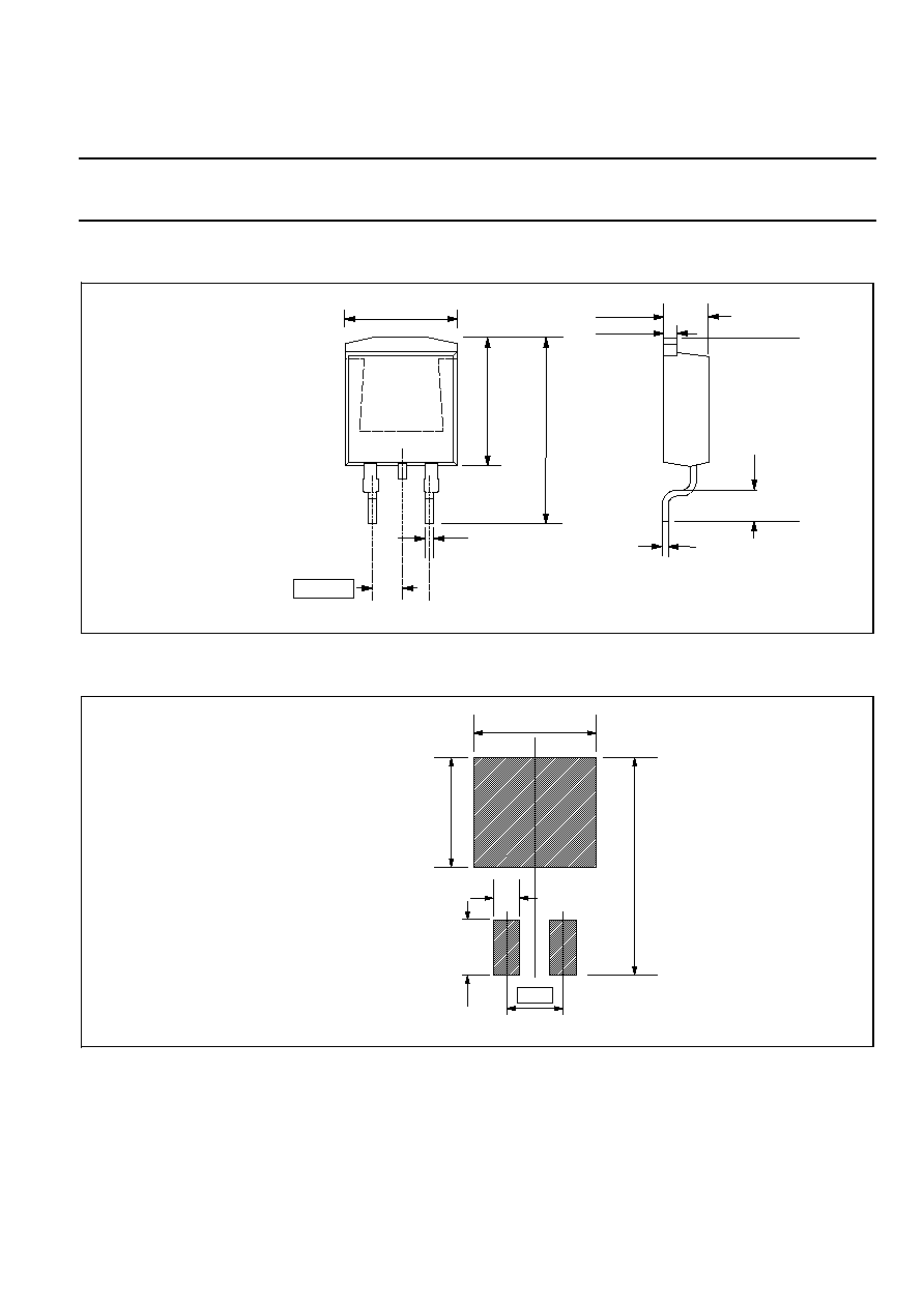
MECHANICAL DATA
Dimensions in mm
Net Mass: 1.4 g
Fig.15. SOT404 : centre pin connected to mounting base.
MOUNTING INSTRUCTIONS
Dimensions in mm
Fig.16. SOT404 : soldering pattern for surface mounting.
Notes
1. Epoxy meets UL94 V0 at 1/8".
11 max
4.5 max
1.4 max
10.3 max
0.5
15.4
2.5
0.85 max
(x2)
2.54 (x2)
17.5
11.5
9.0
5.08
3.8
2.0
October 1998
5
Rev 1.200

Philips Semiconductors
Product specification
Rectifier diode
BYC8B-600
ultrafast, low switching loss
DEFINITIONS
Data sheet status
Objective specification
This data sheet contains target or goal specifications for product development.
Preliminary specification This data sheet contains preliminary data; supplementary data may be published later.
Product specification
This data sheet contains final product specifications.
Limiting values
Limiting values are given in accordance with the Absolute Maximum Rating System (IEC 134). Stress above one
or more of the limiting values may cause permanent damage to the device. These are stress ratings only and
operation of the device at these or at any other conditions above those given in the Characteristics sections of
this specification is not implied. Exposure to limiting values for extended periods may affect device reliability.
Application information
Where application information is given, it is advisory and does not form part of the specification.
©
Philips Electronics N.V. 1998
All rights are reserved. Reproduction in whole or in part is prohibited without the prior written consent of the
copyright owner.
The information presented in this document does not form part of any quotation or contract, it is believed to be
accurate and reliable and may be changed without notice. No liability will be accepted by the publisher for any
consequence of its use. Publication thereof does not convey nor imply any license under patent or other
industrial or intellectual property rights.
LIFE SUPPORT APPLICATIONS
These products are not designed for use in life support appliances, devices or systems where malfunction of these
products can be reasonably expected to result in personal injury. Philips customers using or selling these products
for use in such applications do so at their own risk and agree to fully indemnify Philips for any damages resulting
from such improper use or sale.
October 1998
6
Rev 1.200