 | ÐлекÑÑоннÑй компоненÑ: BYD17D | СкаÑаÑÑ:  PDF PDF  ZIP ZIP |
BYD17_SERIES_4 General purpose controlled avalanche rectifiers
DATA SHEET
Product specification
Supersedes data of 1999 Nov 11
2001 Oct 26
DISCRETE SEMICONDUCTORS
BYD17 series
General purpose
controlled avalanche rectifiers
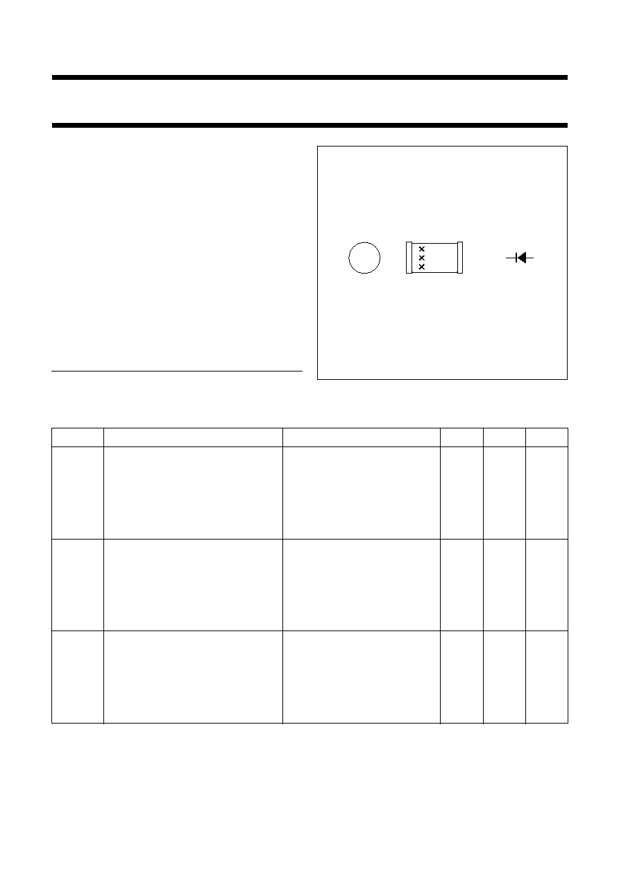
book, halfpage
M3D121
2001 Oct 26
2
Philips Semiconductors
Product specification
General purpose
controlled avalanche rectifiers
BYD17 series
FEATURES
·
Glass passivated
·
High maximum operating temperature
·
Low leakage current
·
Excellent stability
·
Guaranteed avalanche energy absorption capability
·
Shipped in 8 mm embossed tape
·
Smallest surface mount rectifier outline.
DESCRIPTION
Cavity free cylindrical glass package through Implotec
TM
(1)
technology.
This package is hermetically sealed and fatigue free as
coefficients of expansion of all used parts are matched.
(1) Implotec is a trademark of Philips.
olumns
MAM061
k
a
Fig.1 Simplified outline (SOD87) and symbol.
LIMITING VALUES
In accordance with the Absolute Maximum Rating System (IEC 60134).
SYMBOL
PARAMETER
CONDITIONS
MIN.
MAX.
UNIT
V
RRM
repetitive peak reverse voltage
BYD17D
-
200
V
BYD17G
-
400
V
BYD17J
-
600
V
BYD17K
-
800
V
BYD17M
-
1000
V
V
RWM
crest working reverse voltage
BYD17D
-
200
V
BYD17G
-
400
V
BYD17J
-
600
V
BYD17K
-
800
V
BYD17M
-
1000
V
V
R
continuous reverse voltage
BYD17D
-
200
V
BYD17G
-
400
V
BYD17J
-
600
V
BYD17K
-
800
V
BYD17M
-
1000
V

2001 Oct 26
3
Philips Semiconductors
Product specification
General purpose
controlled avalanche rectifiers
BYD17 series
ELECTRICAL CHARACTERISTICS
T
j
= 25
°
C unless otherwise specified.
THERMAL CHARACTERISTICS
Note
1. Device mounted on epoxy-glass printed-circuit board, 1.5 mm thick; thickness of copper
40
µ
m, see Fig.9.
For more information please refer to the
"General Part of associated Handbook".
I
F(AV)
average forward current
T
tp
= 105
°
C;
averaged over any 20 ms period;
see Figs 2 and 4
-
1.5
A
T
amb
= 65
°
C; PCB mounting (see
Fig.9);
averaged over any 20 ms period;
see Figs 3 and 4
-
0.6
A
I
FSM
non-repetitive peak forward current
t = 10 ms half sinewave;
T
j
= T
j max
prior to surge;
V
R
= V
RRMmax
-
20
A
E
RSM
non-repetitive peak reverse avalanche
energy
L = 120 mH; T
j
= T
j max
prior to
surge; inductive load switched off
-
7
mJ
T
stg
storage temperature
-
65
+175
°
C
T
j
junction temperature
see Fig.5
-
65
+175
°
C
SYMBOL
PARAMETER
CONDITIONS
MIN.
TYP.
MAX.
UNIT
V
F
forward voltage
I
F
= 1 A; T
j
= T
j max;
see Fig.6
-
-
0.93
V
I
F
= 1 A; see Fig.6
-
-
1.05
V
V
(BR)R
reverse avalanche
breakdown voltage
I
R
= 0.1 mA
BYD17D
225
-
-
V
BYD17G
450
-
-
V
BYD17J
650
-
-
V
BYD17K
900
-
-
V
BYD17M
1100
-
-
V
I
R
reverse current
V
R
= V
RRMmax
; see Fig.7
-
-
1
µ
A
V
R
= V
RRMmax
; T
j
= 165
°
C; see Fig.7
-
-
100
µ
A
t
rr
reverse recovery time
when switched from I
F
= 0.5 A to I
R
= 1 A;
measured at I
R
= 0.25 A; see Fig.10
-
3
-
µ
s
C
d
diode capacitance
V
R
= 0 V; f = 1 MHz; see Fig.8
-
21
-
pF
SYMBOL
PARAMETER
CONDITIONS
VALUE
UNIT
R
th j-tp
thermal resistance from junction to tie-point
30
K/W
R
th j-a
thermal resistance from junction to ambient
note 1
150
K/W
SYMBOL
PARAMETER
CONDITIONS
MIN.
MAX.
UNIT
2001 Oct 26
4
Philips Semiconductors
Product specification
General purpose
controlled avalanche rectifiers
BYD17 series
GRAPHICAL DATA
Fig.2
Maximum permissible average forward
current as a function of tie-point
temperature (including losses due to
reverse leakage).
a = 1.57; V
R
= V
RRMmax
;
= 0.5.
handbook, halfpage
0
200
160
120
0
MBH394
1
2
3
80
40
Ttp (
°
C)
IF(AV)
(A)
0
200
160
120
0
MSC293
0.2
0.4
0.6
0.8
1.0
80
40
Tamb (
°
C)
IF(AV)
(A)
Fig.3
Maximum permissible average forward
current as a function of ambient
temperature (including losses due to
reverse leakage).
a = 1.57; V
R
= V
RRMmax
;
= 0.5.
Device mounted as shown in Fig.9.
Fig.4
Maximum steady state power dissipation
(forward plus leakage current losses,
excluding switching losses) as a function of
average forward current.
a = I
F(RMS)
/I
F(AV)
; V
R
= V
RRMmax
;
= 0.5.
handbook, halfpage
0
1.6
1.2
0
MBH395
0.5
1.0
1.5
2.0
2.5
0.8
0.4
P
(W)
IF(AV) (A)
a = 3
1.42
1.57
2.5
2
Solid line = V
R
.
Dotted line = V
RRM
;
= 0.5.
Fig.5
Maximum permissible junction temperature
as a function of reverse voltage.
handbook, halfpage
0
D
G
J
K
M
400
800
1200
200
0
100
50
150
MGC736
Tj
VR, VRRM (V)
( C)
o
2001 Oct 26
5
Philips Semiconductors
Product specification
General purpose
controlled avalanche rectifiers
BYD17 series
Solid line: T
j
= 25
°
C.
Dotted line: T
j
= 175
°
C.
Fig.6
Forward current as a function of forward
voltage; maximum values.
handbook, halfpage
0
6
4
2
0
2
1
MBG048
IF
(A)
VF (V)
Fig.7
Reverse current as a function of junction
temperature; maximum values.
handbook, halfpage
200
0
10
3
MGC739
10
2
10
1
160
120
40
80
(
µ
A)
I
R
T
j
(
o
C)
V
R
= V
RRMmax.
Fig.8
Diode capacitance as a function of reverse
voltage; typical values.
f = 1 MHz; T
j
= 25
°
C.
handbook, halfpage
1
MGC740
10
10
2
10
3
1
10
2
10
(pF)
C
d
V
R
(V)
MSB213
4.5
2.5
1.25
50
50
Fig.9
Printed-circuit board for surface mounting.
Dimensions in mm.
2001 Oct 26
6
Philips Semiconductors
Product specification
General purpose
controlled avalanche rectifiers
BYD17 series
handbook, full pagewidth
10
1
50
25 V
DUT
MAM057
+
t rr
0.5
0
0.5
1.0
IF
(A)
IR
(A)
t
0.25
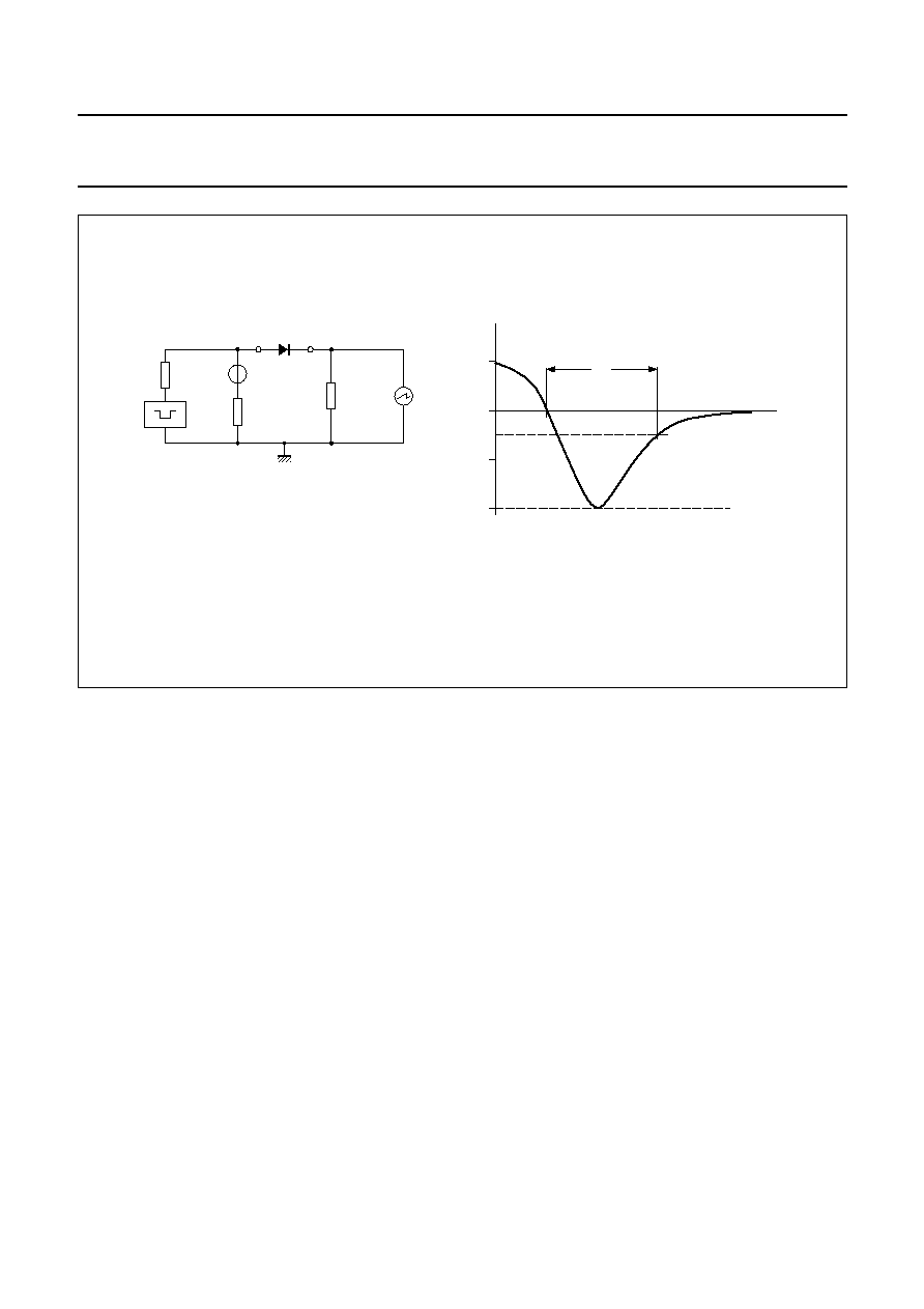
Fig.10 Test circuit and reverse recovery time waveform and definition.
Input impedance oscilloscope: 1 M
, 22 pF; t
r
7 ns.
Source impedance: 50
; t
r
15 ns.
2001 Oct 26
7
Philips Semiconductors
Product specification
General purpose
controlled avalanche rectifiers
BYD17 series
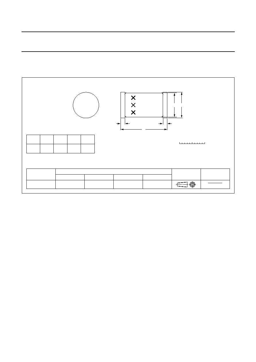
PACKAGE OUTLINE
REFERENCES
OUTLINE
VERSION
EUROPEAN
PROJECTION
ISSUE DATE
IEC
JEDEC
EIAJ
SOD87
100H03
99-03-31
99-06-04
Hermetically sealed glass surface mounted package;
Implotec
TM(1)
technology; 2 connectors
SOD87
UNIT
D
mm
2.1
2.0
2.0
1.8
3.7
3.3
0.3
D1
H
L
DIMENSIONS (mm are the original dimensions)
H
D
D1
L
L
(2)
0
1
2 mm
scale
Notes
1. Implotec is a trademark of Philips.
2. The marking indicates the cathode.
k
a

2001 Oct 26
8
Philips Semiconductors
Product specification
General purpose
controlled avalanche rectifiers
BYD17 series
DATA SHEET STATUS
Notes
1. Please consult the most recently issued data sheet before initiating or completing a design.
2. The product status of the device(s) described in this data sheet may have changed since this data sheet was
published. The latest information is available on the Internet at URL http://www.semiconductors.philips.com.
DATA SHEET STATUS
(1)
PRODUCT
STATUS
(2)
DEFINITIONS
Objective data
Development
This data sheet contains data from the objective specification for product
development. Philips Semiconductors reserves the right to change the
specification in any manner without notice.
Preliminary data
Qualification
This data sheet contains data from the preliminary specification.
Supplementary data will be published at a later date. Philips
Semiconductors reserves the right to change the specification without
notice, in order to improve the design and supply the best possible
product.
Product data
Production
This data sheet contains data from the product specification. Philips
Semiconductors reserves the right to make changes at any time in order
to improve the design, manufacturing and supply. Changes will be
communicated according to the Customer Product/Process Change
Notification (CPCN) procedure SNW-SQ-650A.
DEFINITIONS
Short-form specification
The data in a short-form
specification is extracted from a full data sheet with the
same type number and title. For detailed information see
the relevant data sheet or data handbook.
Limiting values definition
Limiting values given are in
accordance with the Absolute Maximum Rating System
(IEC 60134). Stress above one or more of the limiting
values may cause permanent damage to the device.
These are stress ratings only and operation of the device
at these or at any other conditions above those given in the
Characteristics sections of the specification is not implied.
Exposure to limiting values for extended periods may
affect device reliability.
Application information
Applications that are
described herein for any of these products are for
illustrative purposes only. Philips Semiconductors make
no representation or warranty that such applications will be
suitable for the specified use without further testing or
modification.
DISCLAIMERS
Life support applications
These products are not
designed for use in life support appliances, devices, or
systems where malfunction of these products can
reasonably be expected to result in personal injury. Philips
Semiconductors customers using or selling these products
for use in such applications do so at their own risk and
agree to fully indemnify Philips Semiconductors for any
damages resulting from such application.
Right to make changes
Philips Semiconductors
reserves the right to make changes, without notice, in the
products, including circuits, standard cells, and/or
software, described or contained herein in order to
improve design and/or performance. Philips
Semiconductors assumes no responsibility or liability for
the use of any of these products, conveys no licence or title
under any patent, copyright, or mask work right to these
products, and makes no representations or warranties that
these products are free from patent, copyright, or mask
work right infringement, unless otherwise specified.

2001 Oct 26
9
Philips Semiconductors
Product specification
General purpose
controlled avalanche rectifiers
BYD17 series
NOTES

2001 Oct 26
10
Philips Semiconductors
Product specification
General purpose
controlled avalanche rectifiers
BYD17 series
NOTES

2001 Oct 26
11
Philips Semiconductors
Product specification
General purpose
controlled avalanche rectifiers
BYD17 series
NOTES

© Koninklijke Philips Electronics N.V. 2001
SCA73
All rights are reserved. Reproduction in whole or in part is prohibited without the prior written consent of the copyright owner.
The information presented in this document does not form part of any quotation or contract, is believed to be accurate and reliable and may be changed
without notice. No liability will be accepted by the publisher for any consequence of its use. Publication thereof does not convey nor imply any license
under patent- or other industrial or intellectual property rights.
Philips Semiconductors a worldwide company
Contact information
For additional information please visit http://www.semiconductors.philips.com.
Fax: +31 40 27 24825
For sales offices addresses send e-mail to: sales.addresses@www.semiconductors.philips.com.
Printed in The Netherlands
613510/04/pp
12
Date of release:
2001 Oct 26
Document order number:
9397 750 08864
Document Outline
- FEATURES
- DESCRIPTION
- LIMITING VALUES
- ELECTRICAL CHARACTERISTICS
- THERMAL CHARACTERISTICS
- GRAPHICAL DATA
- PACKAGE OUTLINE
- DATA SHEET STATUS
- DEFINITIONS
- DISCLAIMERS