Philips Semiconductors
Product specification
Three quadrant triacs
BTA212X series B
high commutation
GENERAL DESCRIPTION
QUICK REFERENCE DATA
Glass passivated high commutation
SYMBOL
PARAMETER
MAX.
MAX.
MAX. UNIT
triacs in a full pack, plastic envelope
intended for use in circuits where high
BTA212X-
500B
600B
800B
static and dynamic dV/dt and high
V
DRM
Repetitive peak off-state
500
600
800
V
dI/dt can occur. These devices will
voltages
commutate the full rated rms current
I
T(RMS)
RMS on-state current
12
12
12
A
at
the
maximum
rated
junction
I
TSM
Non-repetitive peak on-state
95
95
95
A
temperature, without the aid of a
current
snubber.
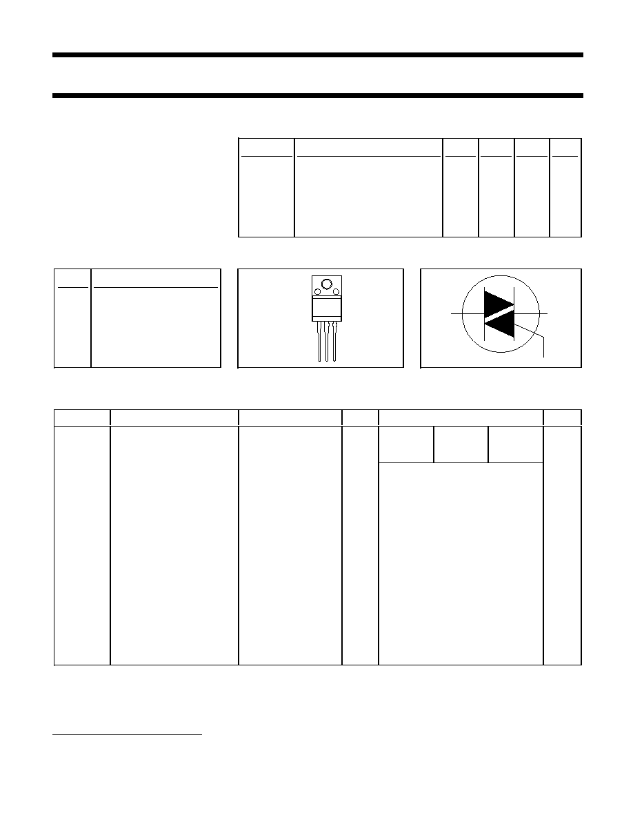
PINNING - SOT186A
PIN CONFIGURATION
SYMBOL
PIN
DESCRIPTION
1
main terminal 1
2
main terminal 2
3
gate
case
isolated
LIMITING VALUES
Limiting values in accordance with the Absolute Maximum System (IEC 134).
SYMBOL
PARAMETER
CONDITIONS
MIN.
MAX.
UNIT
-500
-600
-800
V
DRM
Repetitive peak off-state
-
500
1
600
1
800
V
voltages
I
T(RMS)
RMS on-state current
full sine wave;
-
12
A
T
hs
56 ∞C
I
TSM
Non-repetitive peak
full sine wave;
on-state current
T
j
= 25 ∞C prior to
surge
t = 20 ms
-
95
A
t = 16.7 ms
-
105
A
I
2
t
I
2
t for fusing
t = 10 ms
-
45
A
2
s
dI
T
/dt
Repetitive rate of rise of
I
TM
= 20 A; I
G
= 0.2 A;
100
A/
µ
s
on-state current after
dI
G
/dt = 0.2 A/
µ
s
triggering
I
GM
Peak gate current
-
2
A
V
GM
Peak gate voltage
-
5
V
P
GM
Peak gate power
-
5
W
P
G(AV)
Average gate power
over any 20 ms
-
0.5
W
period
T
stg
Storage temperature
-40
150
∞C
T
j
Operating junction
-
125
∞C
temperature
T1
T2
G
1 2 3
case
1 Although not recommended, off-state voltages up to 800V may be applied without damage, but the triac may
switch to the on-state. The rate of rise of current should not exceed 15 A/
µ
s.
September 1997
1
Rev 1.200

Philips Semiconductors
Product specification
Three quadrant triacs
BTA212X series B
high commutation
ISOLATION LIMITING VALUE & CHARACTERISTIC
T
hs
= 25 ∞C unless otherwise specified
SYMBOL
PARAMETER
CONDITIONS
MIN.
TYP.
MAX.
UNIT
V
isol
R.M.S. isolation voltage from all
f = 50-60 Hz; sinusoidal
-
2500
V
three terminals to external
waveform;
heatsink
R.H.
65% ; clean and dustfree
C
isol
Capacitance from T2 to external f = 1 MHz
-
10
-
pF
heatsink
THERMAL RESISTANCES
SYMBOL
PARAMETER
CONDITIONS
MIN.
TYP.
MAX.
UNIT
R
th j-hs
Thermal resistance
full or half cycle
junction to heatsink
with heatsink compound
-
-
4.0
K/W
without heatsink compound
-
-
5.5
K/W
R
th j-a
Thermal resistance
in free air
-
55
-
K/W
junction to ambient
STATIC CHARACTERISTICS
T
j
= 25 ∞C unless otherwise stated
SYMBOL
PARAMETER
CONDITIONS
MIN.
TYP.
MAX.
UNIT
I
GT
Gate trigger current
2
V
D
= 12 V; I
T
= 0.1 A
T2+ G+
2
18
50
mA
T2+ G-
2
21
50
mA
T2- G-
2
34
50
mA
I
L
Latching current
V
D
= 12 V; I
GT
= 0.1 A
T2+ G+
-
31
60
mA
T2+ G-
-
34
90
mA
T2- G-
-
30
60
mA
I
H
Holding current
V
D
= 12 V; I
GT
= 0.1 A
-
31
60
mA
V
T
On-state voltage
I
T
= 17 A
-
1.3
1.6
V
V
GT
Gate trigger voltage
V
D
= 12 V; I
T
= 0.1 A
-
0.7
1.5
V
V
D
= 400 V; I
T
= 0.1 A; T
j
= 125 ∞C
0.25
0.4
-
V
I
D
Off-state leakage current
V
D
= V
DRM(max)
; T
j
= 125 ∞C
-
0.1
0.5
mA
DYNAMIC CHARACTERISTICS
T
j
= 25 ∞C unless otherwise stated
SYMBOL
PARAMETER
CONDITIONS
MIN.
TYP.
MAX.
UNIT
dV
D
/dt
Critical rate of rise of
V
DM
= 67% V
DRM(max)
; T
j
= 125 ∞C;
1000
4000
-
V/
µ
s
off-state voltage
exponential waveform; gate open circuit
dI
com
/dt
Critical rate of change of
V
DM
= 400 V; T
j
= 125 ∞C; I
T(RMS)
= 12 A;
-
24
-
A/ms
commutating current
without snubber; gate open circuit
t
gt
Gate controlled turn-on
I
TM
= 12 A; V
D
= V
DRM(max)
; I
G
= 0.1 A;
-
2
-
µ
s
time
dI
G
/dt = 5 A/
µ
s
2 Device does not trigger in the T2-, G+ quadrant.
September 1997
2
Rev 1.200

Philips Semiconductors
Product specification
Three quadrant triacs
BTA212X series B
high commutation
Fig.1. Maximum on-state dissipation, P
tot
, versus rms
on-state current, I
T(RMS)
, where
= conduction angle.
Fig.2. Maximum permissible non-repetitive peak
on-state current I
TSM
, versus pulse width t
p
, for
sinusoidal currents, t
p
20ms.
Fig.3. Maximum permissible non-repetitive peak
on-state current I
TSM
, versus number of cycles, for
sinusoidal currents, f = 50 Hz.
Fig.4. Maximum permissible rms current I
T(RMS)
,
versus heatsink temperature T
hs
.
Fig.5. Maximum permissible repetitive rms on-state
current I
T(RMS)
, versus surge duration, for sinusoidal
currents, f = 50 Hz; T
hs
56∞C.
Fig.6. Normalised gate trigger voltage
V
GT
(T
j
)/ V
GT
(25∞C), versus junction temperature T
j
.
0
5
10
15
0
5
10
15
20
= 180
120
90
60
30
BT138
IT(RMS) / A
Ptot / W
Ths(max) / C
125
105
85
65
45
1
-50
0
50
100
150
0
5
10
15
BT138X
56 C
Ths / C
IT(RMS) / A
10us
100us
1ms
10ms
100ms
10
100
1000
BTA212
T / s
ITSM / A
T
ITSM
time
I
Tj initial = 25 C max
T
dI /dt limit
T
0.01
0.1
1
10
0
5
10
15
20
25
BT138
surge duration / s
IT(RMS) / A
1
10
100
1000
0
20
40
60
80
100
BT138
Number of cycles at 50Hz
ITSM / A
T
ITSM
time
I
Tj initial = 25 C max
T
-50
0
50
100
150
0.4
0.6
0.8
1
1.2
1.4
1.6
BT136
Tj / C
VGT(Tj)
VGT(25 C)
September 1997
3
Rev 1.200

Philips Semiconductors
Product specification
Three quadrant triacs
BTA212X series B
high commutation
Fig.7. Normalised gate trigger current
I
GT
(T
j
)/ I
GT
(25∞C), versus junction temperature T
j
.
Fig.8. Normalised latching current I
L
(T
j
)/ I
L
(25∞C),
versus junction temperature T
j
.
Fig.9. Normalised holding current I
H
(T
j
)/ I
H
(25∞C),
versus junction temperature T
j
.
Fig.10. Typical and maximum on-state characteristic.
Fig.11. Transient thermal impedance Z
th j-hs
, versus
pulse width t
p
.
Fig.12. Typical critical rate of change of commutating
current dI
com
/dt versus junction temperature.
-50
0
50
100
150
0
0.5
1
1.5
2
2.5
3
BTA212
Tj / C
T2+ G+
T2+ G-
T2- G-
IGT(Tj)
IGT(25 C)
0
0.5
1
1.5
2
2.5
3
0
10
20
30
40
BT138
VT / V
IT / A
Tj = 125 C
Tj = 25 C
typ
max
Vo = 1.175 V
Rs = 0.0316 Ohms
-50
0
50
100
150
0
0.5
1
1.5
2
2.5
3
TRIAC
Tj / C
IL(Tj)
IL(25 C)
0.001
0.01
0.1
1
10
BT138
tp / s
Zth j-hs (K/W)
10us
0.1ms
1ms
10ms
0.1s
1s
10s
t
p
P
t
D
bidirectional
unidirectional
with heatsink compound
without heatsink compound
-50
0
50
100
150
0
0.5
1
1.5
2
2.5
3
TRIAC
Tj / C
IH(Tj)
IH(25C)
20
40
60
80
100
120
140
1
10
100
1000
BTA212
Tj / C
dIcom/dt (A/ms)
September 1997
4
Rev 1.200
Philips Semiconductors
Product specification
Three quadrant triacs
BTA212X series B
high commutation
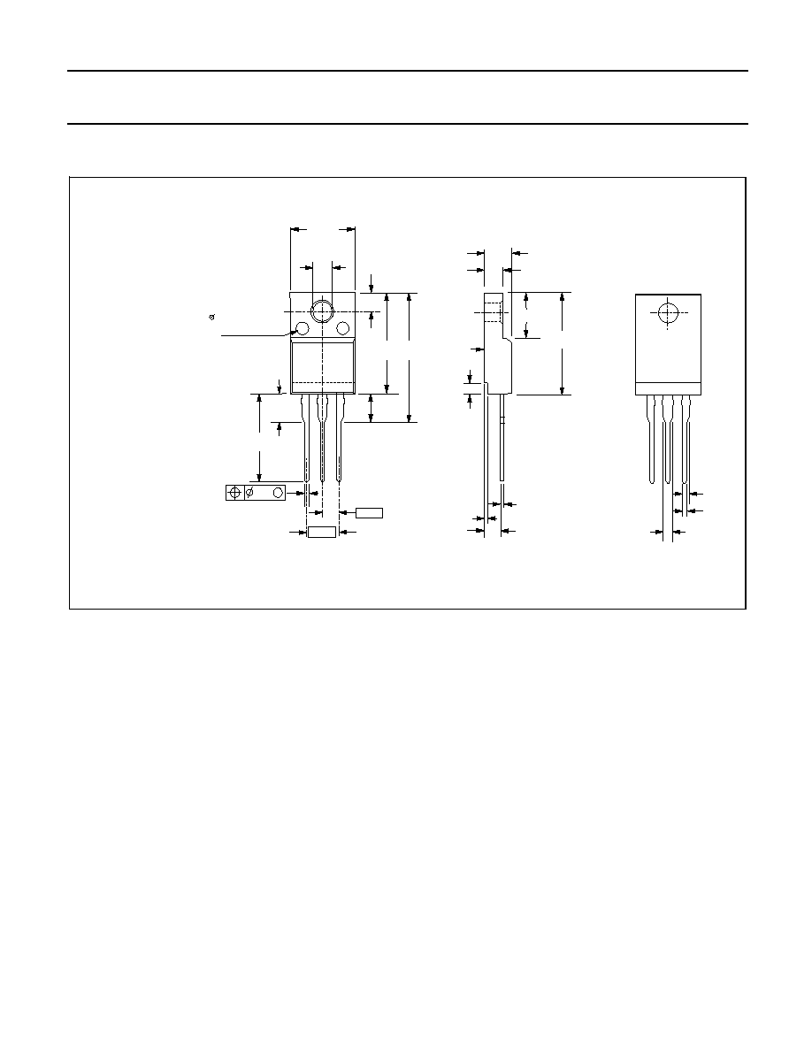
MECHANICAL DATA
Dimensions in mm
Net Mass: 2 g
Fig.13. SOT186A; The seating plane is electrically isolated from all terminals.
Notes
1. Refer to mounting instructions for F-pack envelopes.
2. Epoxy meets UL94 V0 at 1/8".
10.3
max
3.2
3.0
4.6
max
2.9 max
2.8
seating
plane
6.4
15.8
max
0.6
2.5
2.54
5.08
1
2
3
3 max.
not tinned
3
0.5
2.5
0.9
0.7
M
0.4
15.8
max.
19
max.
13.5
min.
Recesses (2x)
2.5
0.8 max. depth
1.0 (2x)
1.3
September 1997
5
Rev 1.200

Philips Semiconductors
Product specification
Three quadrant triacs
BTA212X series B
high commutation
DEFINITIONS
Data sheet status
Objective specification
This data sheet contains target or goal specifications for product development.
Preliminary specification This data sheet contains preliminary data; supplementary data may be published later.
Product specification
This data sheet contains final product specifications.
Limiting values
Limiting values are given in accordance with the Absolute Maximum Rating System (IEC 134). Stress above one
or more of the limiting values may cause permanent damage to the device. These are stress ratings only and
operation of the device at these or at any other conditions above those given in the Characteristics sections of
this specification is not implied. Exposure to limiting values for extended periods may affect device reliability.
Application information
Where application information is given, it is advisory and does not form part of the specification.
©
Philips Electronics N.V. 1997
All rights are reserved. Reproduction in whole or in part is prohibited without the prior written consent of the
copyright owner.
The information presented in this document does not form part of any quotation or contract, it is believed to be
accurate and reliable and may be changed without notice. No liability will be accepted by the publisher for any
consequence of its use. Publication thereof does not convey nor imply any license under patent or other
industrial or intellectual property rights.
LIFE SUPPORT APPLICATIONS
These products are not designed for use in life support appliances, devices or systems where malfunction of these
products can be reasonably expected to result in personal injury. Philips customers using or selling these products
for use in such applications do so at their own risk and agree to fully indemnify Philips for any damages resulting
from such improper use or sale.
September 1997
6
Rev 1.200