1999 Jun 04
2
Philips Semiconductors
Product specification
Voltage regulator diodes
BZX399 series
FEATURES
∑
Total power dissipation: max. 300 mW
∑
Tolerance:
±
5%
∑
Working voltage range: nom. 1.8 to 43 V (E24 range)
∑
Improved I
Z
/V
Z
characteristic at low currents
(I
Z
= 50
µ
A). This results in a noise free and sharp
breakdown knee.
APPLICATIONS
∑
General regulation functions, where low noise at low
currents is required
∑
Low power consumption applications
(e.g. hand-held applications).
DESCRIPTION
Low-power low noise voltage regulator diodes in SOD323
plastic SMD package.
The diodes are available in the normalized E24
±
5%
tolerance range. The series consists of 34 types with
nominal working voltages from 1.8 to 43 V.
PINNING
PIN
DESCRIPTION
1
cathode
2
anode
Fig.1 Simplified outline (SOD323) and symbol.
handbook, halfpage
,
1
2
Top view
MAM387
MARKING
TYPE NUMBER
MARKING
CODE
TYPE NUMBER
MARKING
CODE
TYPE NUMBER
MARKING
CODE
TYPE NUMBER
MARKING
CODE
BZX399-C1V8
B1
BZX399-C4V3
B0
BZX399-C10
BJ
BZX399-C24
BT
BZX399-C2V0
B2
BZX399-C4V7
BA
BZX399-C11
BK
BZX399-C27
BU
BZX399-C2V2
B3
BZX399-C5V1
BB
BZX399-C12
BL
BZX399-C30
BV
BZX399-C2V4
B4
BZX399-C5V6
BC
BZX399-C13
BM
BZX399-C33
BW
BZX399-C2V7
B5
BZX399-C6V2
BD
BZX399-C15
BN
BZX399-C36
BX
BZX399-C3V0
B6
BZX399-C6V8
BE
BZX399-C16
BP
BZX399-C39
BY
BZX399-C3V3
B7
BZX399-C7V5
BF
BZX399-C18
BQ
BZX399-C43
BZ
BZX399-C3V6
B8
BZX399-C8V2
BG
BZX399-C20
BR
BZX399-C3V9
B9
BZX399-C9V1
BH
BZX399-C22
BS

1999 Jun 04
3
Philips Semiconductors
Product specification
Voltage regulator diodes
BZX399 series
LIMITING VALUES
In accordance with the Absolute Maximum Rating System (IEC 134).
Note
1. Device mounted on a FR4 printed circuit-board.
SYMBOL
PARAMETER
CONDITIONS
MIN.
MAX.
UNIT
I
F
continuous forward current
-
250
mA
I
ZSM
non-repetitive peak reverse current
t
p
= 100
µ
s; square wave;
T
amb
= 25
∞
C prior to surge
see Tables 1 and 2
P
tot
total power dissipation
T
amb
= 25
∞
C; note 1
-
300
mW
T
stg
storage temperature
-
65
+150
∞
C
T
j
junction temperature
-
150
∞
C
ELECTRICAL CHARACTERISTICS
Total BZX399-C series
T
j
= 25
∞
C unless otherwise specified.
SYMBOL
PARAMETER
CONDITIONS
MAX.
UNIT
V
F
forward voltage
I
F
= 10 mA; see Fig.5
0.9
V
I
F
= 100 mA; see Fig.5
1.0
V
I
R
reverse current
BZX399-C1V8
V
R
= 1 V
2
µ
A
BZX399-C2V0
V
R
= 1 V
1
µ
A
BZX399-C2V2
V
R
= 1 V
0.5
µ
A
BZX399-C2V4
V
R
= 1 V
0.2
µ
A
BZX399-C2V7
V
R
= 1 V
0.05
µ
A
BZX399-C3V0
V
R
= 1 V
0.02
µ
A
BZX399-C3V3
V
R
= 2 V
2
µ
A
BZX399-C3V6
V
R
= 2 V
1
µ
A
BZX399-C3V9
V
R
= 2 V
0.5
µ
A
BZX399-C4V3
V
R
= 2 V
0.1
µ
A
BZX399-C4V7
V
R
= 3 V
2
µ
A
BZX399-C5V1
V
R
= 3 V
1
µ
A
BZX399-C5V6
V
R
= 4 V
1
µ
A
BZX399-C6V2
V
R
= 5 V
0.1
µ
A
BZX399-C6V8
V
R
= 5 V
0.01
µ
A
BZX399-C7V5
V
R
= 5 V
0.1
µ
A
BZX399-C8V2
V
R
= 6 V
0.2
µ
A
BZX399-C9V1
V
R
= 7 V
0.1
µ
A
BZX399-C10
V
R
= 7 V
0.1
µ
A
BZX399-C11
V
R
= 8 V
0.05
µ
A
BZX399-C12
V
R
= 9 V
0.05
µ
A
BZX399-C13
V
R
= 10 V
0.05
µ
A
BZX399-C15 to 43
V
R
= 0.7V
Znom
0.01
µ
A

1999 Jun 04
5
Philips Semiconductors
Product specification
Voltage regulator diodes
BZX399 series
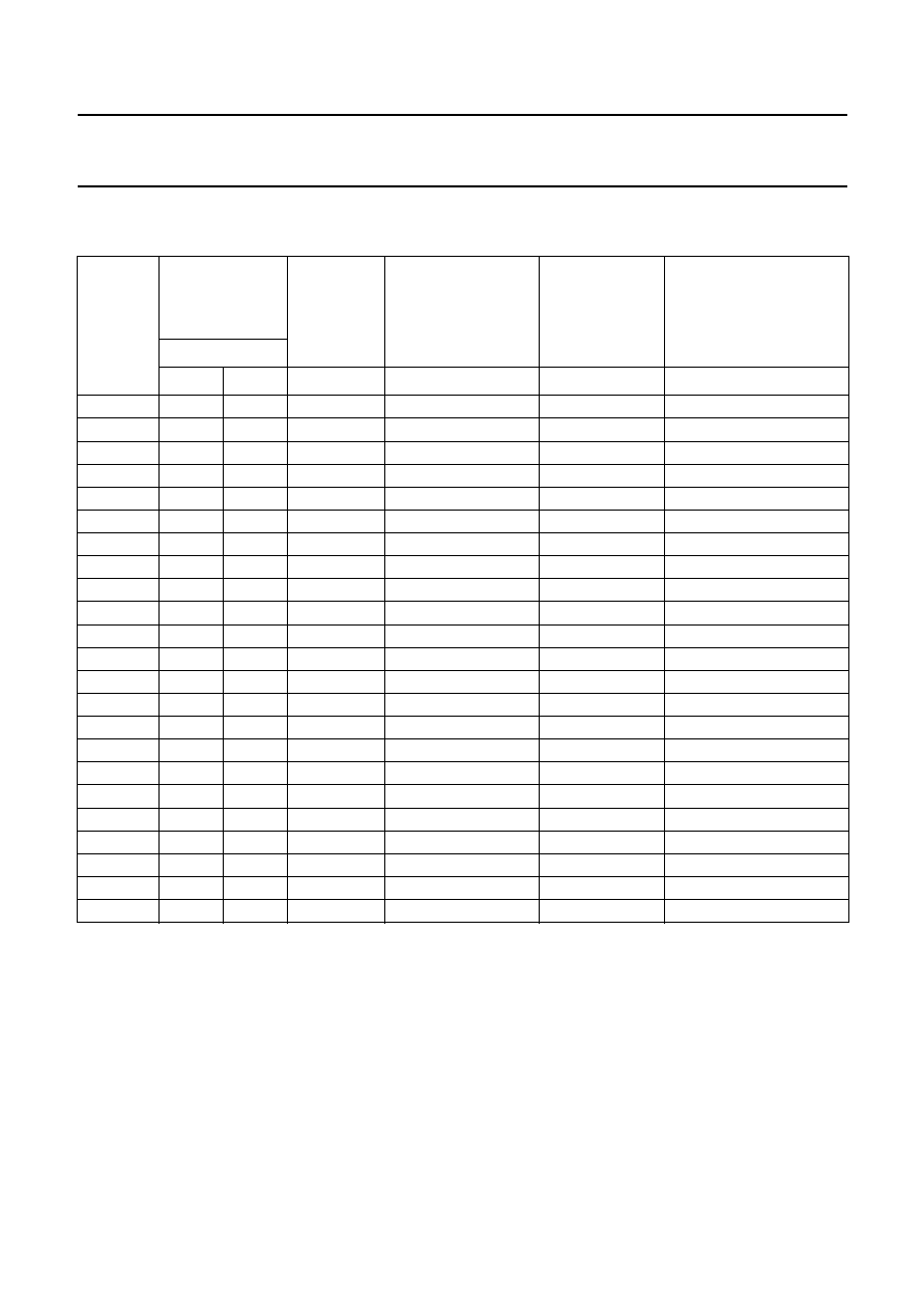
Table 2
Per type BZX399-C16 to C43
T
j
= 25
∞
C unless otherwise specified.
Note
1.
V
Z
= V
Z
at 100
µ
A minus V
Z
at 10
µ
A.
THERMAL CHARACTERISTICS
Notes
1. Device mounted on a FR4 printed circuit-board.
2. Soldering point of the cathode tab.
BZX399- C
XXX
WORKING
VOLTAGE
V
Z
(V)
I
Z
= 50
µ
A
VOLTAGE
CHANGE
V
Z
(V)
(note 1)
TEMP. COEFF.
S
Z
(mV/K)
I
Z
= 50
µ
A
(see Fig.4)
DIODE CAP.
C
d
(pF)
at f = 1 MHz;
V
R
= 0 V
NON-REPETITIVE PEAK
REVERSE CURRENT
I
ZSM
(A) at t
p
= 100
µ
s;
T
amb
= 25
∞
C
Tol.
±
5%
MIN.
MAX.
MAX.
TYP.
MAX.
MAX.
16
15.20
16.80
0.16
11.4
95
1.5
18
17.10
18.90
0.18
13.3
95
1.5
20
19.00
21.00
0.20
15.3
90
1.5
22
20.90
23.10
0.22
17.2
85
1.25
24
22.80
25.20
0.24
19.2
80
1.25
27
25.65
28.35
0.27
22.0
75
1.0
30
28.50
31.50
0.30
25.2
65
1.0
33
31.35
34.65
0.30
28.5
60
0.9
36
34.20
37.80
0.30
32.0
60
0.8
39
37.05
40.95
0.30
35.1
60
0.7
43
40.85
45.15
0.30
39.4
55
0.6
SYMBOL
PARAMETER
CONDITIONS
VALUE
UNIT
R
th j-a
thermal resistance from junction to ambient
note 1
415
K/W
R
th j-s
thermal resistance from junction to soldering point note 2
110
K/W