CBTV4010 10-bit DDR SDRAM mux/bus switch

Philips
Semiconductors
CBTV4010
10-bit DDR SDRAM mux/bus switch
Product data
File under Integrated Circuits -- ICL03
2002 Feb 19
INTEGRATED CIRCUITS
Philips Semiconductors
Product data
CBTV4010
10-bit DDR SDRAM mux/bus switch
2
2002 Feb 19
853-2315 27756
FEATURES
·
Enable signal is SSTL_2 compatible
·
Optimized for use in Double Data Rate (DDR) SDRAM
applications
·
Designed to be used with 400 Mbps/200 MHz DDR data bus
·
Switch on resistance is designed to eliminate the need for series
resistor to DDR SDRAM
·
20
on resistance
·
Internal 100
pull-down resistors
·
Low differential skew
·
Matched rise/fall slew rate
·
Low cross-talk data-data/data-DQM
·
Independent DIMM control lines
·
Latch-up protection exceeds 500 mA per JESD78
·
ESD protection exceeds 2000 V HBM per JESD22-A114,
200 V MM per JESD22-A115 and 1000 V CDM per JESD22-C101
DESCRIPTION
This 10-bit bus switch is designed for 2.3 V to 2.7 V V
CC
operation
and SSTL_2 select input levels.
Each Host port pin is multiplexed to one of four DIMM port pins.
When the S pin is low the corresponding 10-bit bus switch is turned
on. The on-state connects the Host port to the DIMM port through a
20
nominal series resistance. When the S pin is high the switch is
open and a high-impedance state exists between the two ports. The
DIMM port is terminated with a 100
resistor to ground when the
S pin is high. The design is intended to have only one DIMM port
active at any time.
The part incorporates a very low cross-talk design. It has a very low
skew between outputs (< 50 ps) and low skew (< 50 ps) for rising
and falling edges. The part has optional performance in DDR data
bus applications.
Each switch has been optimized for connection to 1 or 2-bank
DIMMs.
The low internal RC time constant of the switch (20
×
7 pF) allows
data transfer to be made with minimal propagation delay.
The CBTV4010 is characterized for operation from 0 to +85
°
C.
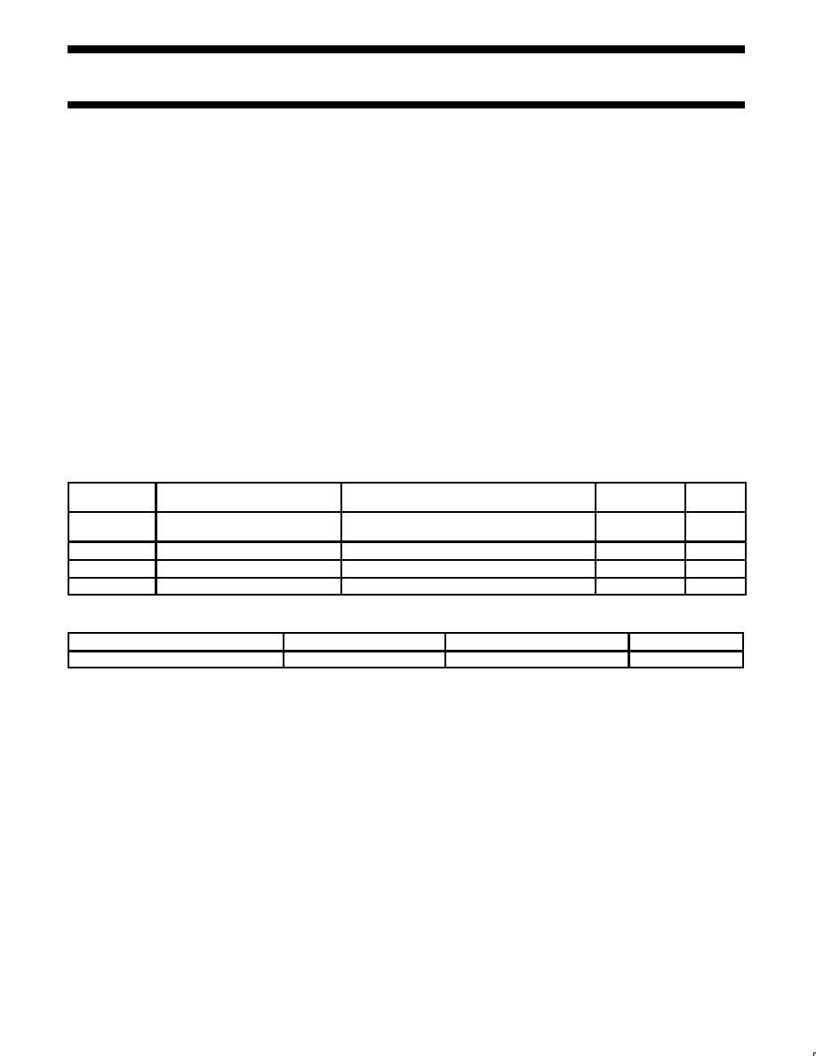
QUICK REFERENCE DATA
SYMBOL
PARAMETER
CONDITIONS
T
amb
= 25
°
C; GND = 0 V
TYPICAL
UNIT
t
PLH
t
PHL
Propagation delay
An to Yn
C
L
= 7 pF; V
CC
= 2.5 V
140
ps
C
IN
Input capacitance control pins
V
I
= 0 V or V
CC
1.8
pF
C
ON
Channel on capacitance
V
in
= 1.5 V
7
pF
I
CCZ
Total supply current
V
CC
= 2.5 V
500
µ
A
ORDERING INFORMATION
PACKAGES
TEMPERATURE RANGE
ORDER CODE
DWG NUMBER
TFBGA64 (Thin Fine Pitch BGA)
0 to +85
°
C
CBTV4010EE
SOT746-1
Philips Semiconductors
Product data
CBTV4010
10-bit DDR SDRAM mux/bus switch
2002 Feb 19
3
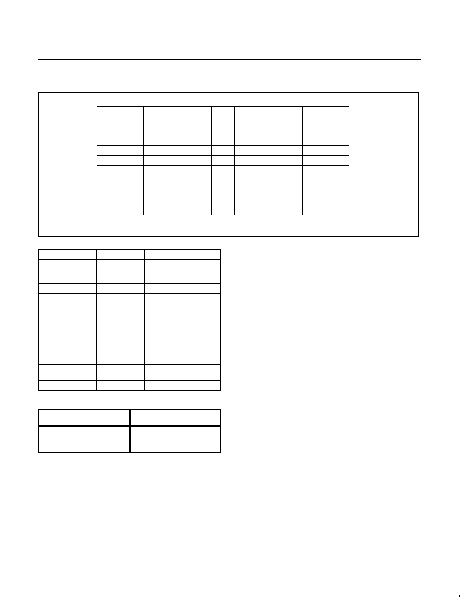
64-BALL BGA CONFIGURATION
A
B
C
D
E
F
G
H
J
K
L
1
2
3
4
5
6
7
8
9
10
11
S2
2DP9
S1
V
DD
S3
GND
HP9
HP8
GND
S0
HP7
3DP6
2DP6
HP6
GND
HP5
GND
HP0
3DP0
0DP1
HP1
GND
HP2
HP3
GND
HP4
SA00589
V
DD
1DP9
0DP9
1DP8
0DP8
3DP7
3DP9
3DP8
2DP8
2DP7
1DP7
0DP7
1DP0
0DP0
2DP0
1DP6
0DP6
1DP1
3DP5
2DP5
2DP1
3DP1
3DP2
0DP3
0DP4
3DP4
1DP5
0DP2
1DP2
2DP2
1DP3
2DP3
3DP3
1DP4
2DP4
0DP5
NC
NC
NOTE: BLANK SPACE INDICATES NO BALL
PIN DESCRIPTION
PIN NUMBER
SYMBOL
NAME AND FUNCTION
B6, B9, C10, F2,
F10, J2, J10, K3,
K6, K9
HP0HP9
Host ports
A2, B1, B3, C2
S0S3
Select
A5, A6, A7, A9,
A10, A11, B5, B7,
B8, B11, C11, D10,
E1, E2, E10, E11,
F1, F11, G1, G2,
G11, H2, H10, J1,
J11, K1, K4, K5,
K8, K10, K11, L1,
L2, L3, L5, L6, L7,
L9, L10, L11
0DP03DP3
0DP13DP1
0DP23DP2
0DP33DP3
0DP43DP4
0DP53DP5
0DP63DP6
0DP73DP7
0DP83DP8
0DP93DP9
DIMM ports
B10, D2, G10, K2,
K7,
GND
Ground
A1, B2
V
DD
Positive supply voltage
FUNCTION TABLE
INPUT
S
FUNCTION
L
Host port = DIMM port
H
Host port = Disconnect
DIMM port = 100
to GND
H = High voltage level
L
= Low voltage level
Philips Semiconductors
Product data
CBTV4010
10-bit DDR SDRAM mux/bus switch
2002 Feb 19
4
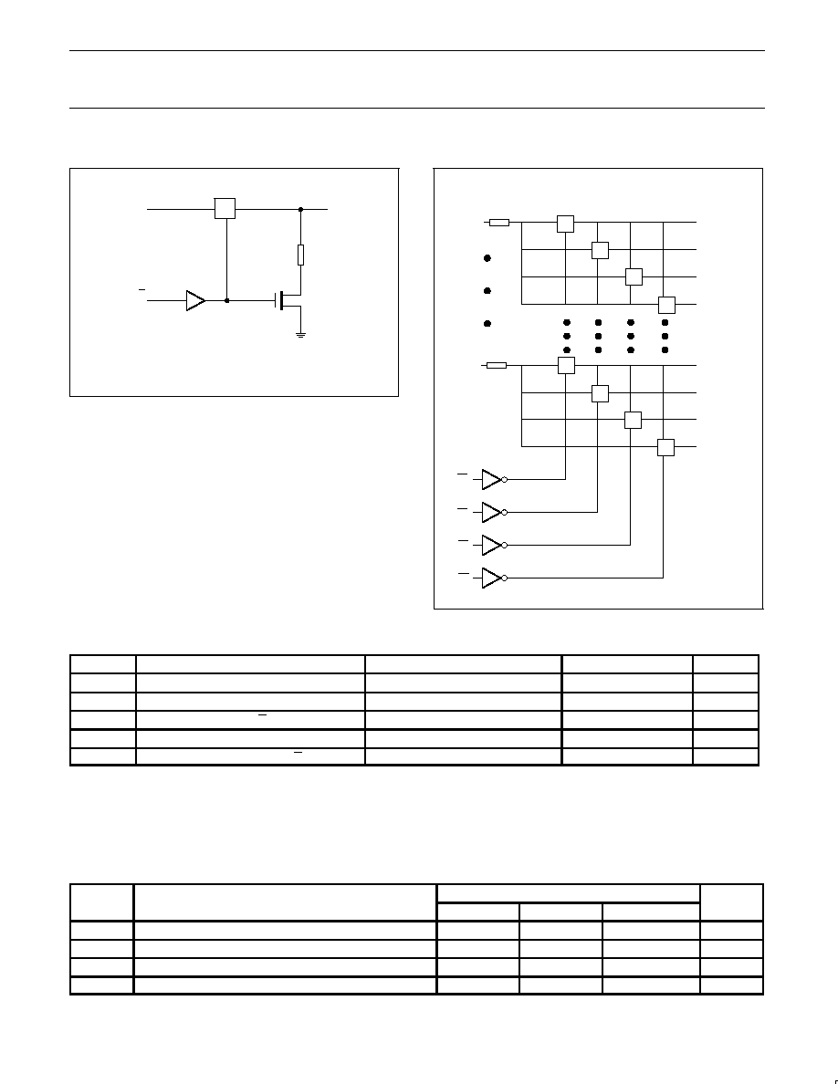
SIMPLIFIED SCHEMATIC, EACH FET SWITCH
Sw
HPx
nDPx
Sn
SW00889
100
A
B
LOGIC DIAGRAM (POSITIVE LOGIC)
Sw
Sw
Sw
Sw
Sw
Sw
Sw
Sw
S0
HP0
HP9
0DP0
SW00901
1DP0
2DP0
3DP0
0DP9
1DP9
2DP9
3DP9
S1
S2
S3
ABSOLUTE MAXIMUM RATINGS
1, 3
SYMBOL
PARAMETER
CONDITIONS
RATING
UNIT
V
CC
DC supply voltage
0.5 to +3.3
V
I
IK
DC input clamp current
V
I/O
< 0
50
mA
V
I
DC input voltage range (S pin only)
2
V
CC
+ 0.3
V
T
stg
Storage temperature range
65 to 150
°
C
V
I
DC input voltage range (except S pin)
2
0.5 to 3.3
V
NOTES:
1. Stresses beyond those listed may cause permanent damage to the device. These are stress ratings only and functional operation of the
device at these or any other conditions beyond those indicated under "recommended operating conditions" is not implied. Exposure to
absolute-maximum-rated conditions for extended periods may affect device reliability.
2. The input and output negative-voltage ratings may be exceeded if the input and output clamp-current ratings are observed.
3. The package thermal impedance is calculated in accordance with JESD 51.
RECOMMENDED OPERATING CONDITIONS
SYMBOL
PARAMETER
LIMITS
UNIT
SYMBOL
PARAMETER
Min
Typ
Max
UNIT
V
CC
DC supply voltage
2.3
2.5
2.7
V
V
IH
High-level input voltage DIMM port and Host
1.6
--
--
V
V
IL
Low-level Input voltage DIMM port and Host
--
--
0.9
V
T
amb
Operating free-air temperature range
0
--
+85
°
C
NOTE:
1. All unused control inputs of the device must be held at V
CC
or GND to ensure proper device operation.
Philips Semiconductors
Product data
CBTV4010
10-bit DDR SDRAM mux/bus switch
2002 Feb 19
5
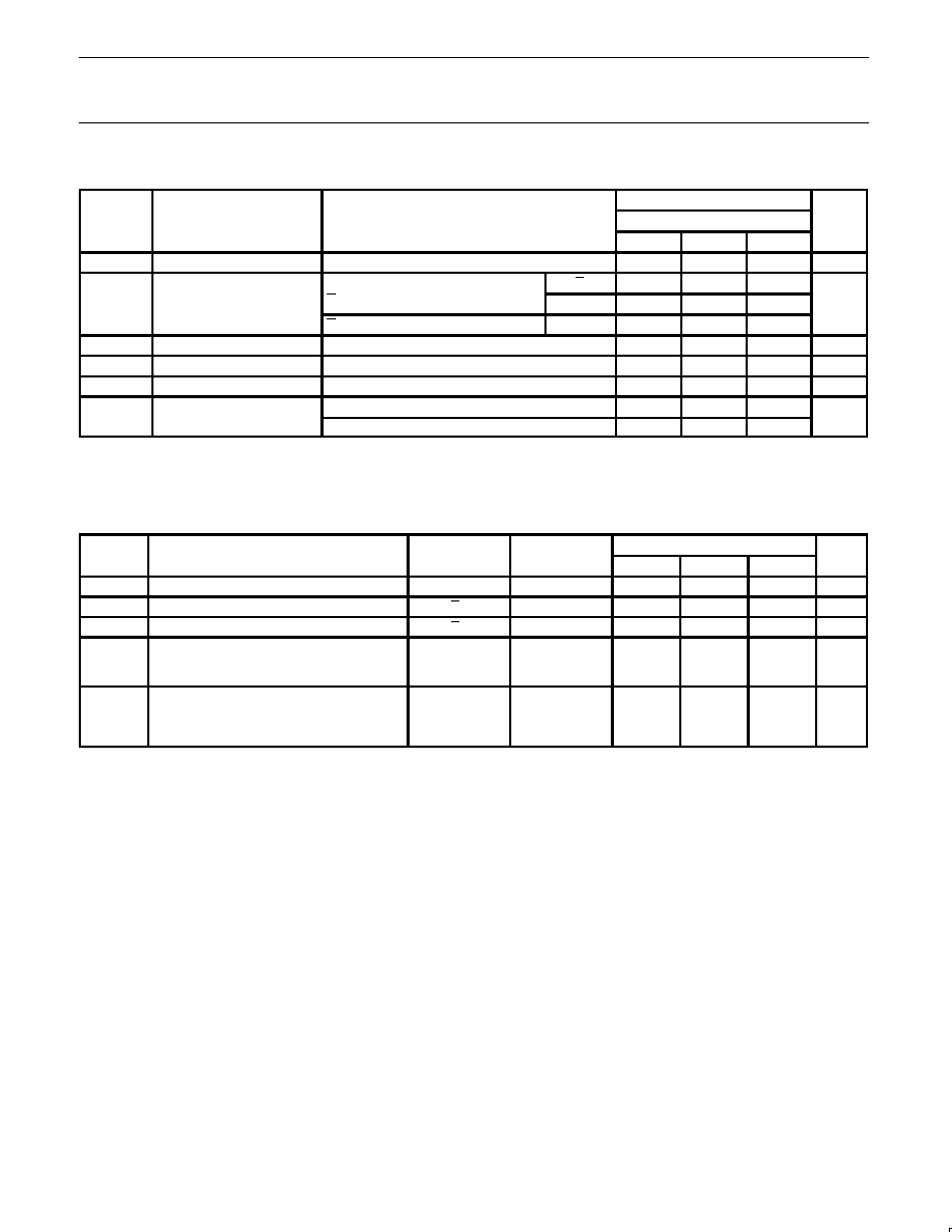
DC ELECTRICAL CHARACTERISTICS
LIMITS
SYMBOL
PARAMETER
TEST CONDITIONS
T
amb
= 0 to +85
°
C
UNIT
Min
Typ
1
Max
V
IK
Input clamp voltage
V
CC
= 2.3 V; I
I
= 18 mA
--
--
1.2
V
V
CC
= 2.5 V; V
I
= V
CC
or GND;
S
--
--
±
100
I
I
Input leakage current
CC
I
CC
S = V
CC
Host port
--
--
±
100
µ
A
S = GND for I
IL (test)
DIMM port
--
--
±
100
I
CC
Quiescent supply current
V
CC
= 2.5 V; I
O
= 0, V
I
= V
CC
or GND
--
0.7
1.5
mA
C
in
Control pin capacitance
V
I
= 2.5 V or 0
--
1.8
3
pF
C
on
Switch on capacitance
V
in
= 1.5 V
--
--
10
pF
r
2
On-resistance
V
CC
= 2.5 V; V
A
= 0.8 V; V
B
= 1.0 V
16
20
30
r
on
2
On-resistance
V
CC
= 2.5 V; V
A
= 1.7 V; V
B
= 1.5 V
16
20
30
NOTES:
1. All typical values are at V
CC
= 2.5 V, T
amb
= 25
°
C
2. Measured by the current between the Host and the DIMM terminals at the indicated voltages on each side of the switch.
3. Capacitance values are measured at a of 10 MHz and a bias voltage 3 V. Capacitance is not production tested.
AC CHARACTERISTICS
SYMBOL
PARAMETER
FROM (INPUT)
TO (OUTPUT)
V
CC
= +2.5 V
±
0.2 V
UNIT
SYMBOL
PARAMETER
FROM (INPUT)
TO (OUTPUT)
Min
Typ
Max
UNIT
t
pd
Propagation delay
1
HPx or xDPx
xDPx or HPx
--
--
140
ps
t
en
enable
S
n
HPx or nDPx
1
--
2
ns
t
dis
disable
S
n
HPx or nDPx
1
--
3
ns
t
osk
Output skew
Any output to any output, Waveform 4
(see note 2)
--
25
50
ps
t
esk
Edge skew
Difference of rising edge propagation delay
to falling edge propagation delay,
Waveform 5 (see note 2)
--
25
50
ps
NOTES:
1. The propagation delay is based on the RC time constant of the typical onstate resistance of the switch and a load capacitance, when driven
by an ideal voltage source (zero output impedance); 20
×
7 pF.
This parameter is not production tested.
2. Skew is not production tested.
Philips Semiconductors
Product data
CBTV4010
10-bit DDR SDRAM mux/bus switch
2002 Feb 19
6
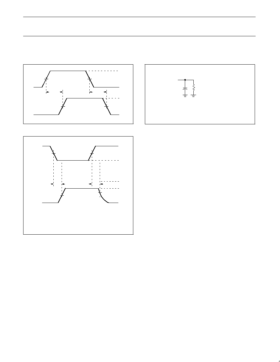
HPx to nDPx AC WAVEFORMS AND TEST CIRCUIT
AC WAVEFORMS
D or H
1.25 V
H or D
t
PLH
t
PHL
1.25 V
1.25 V
1.25 V
2.5 V
0 V
V
OH
V
OL
SA00620
Waveform 1. Input (D or H) to Output (H or D) Propagation
Delays
Sn
(Low-level
enabling
1.25 V
t
PZH
t
PHZ
V
OH
V
OL
V
OH
0.15 V
1.25 V
2.5 V
Note:
The output is high except when disabled by the Sn control.
Output
nDPx
(see Note)
0 V
1.25 V
SA00621
V
OL
Waveform 2. 3-State Output Enable and Disable Times
TEST CIRCUIT HPx to xDPx
C
L
= 30 pF
500
Load Circuit
DEFINITIONS
C
L
=
Load capacitance includes jig and probe capacitance
From Output
Under Test
SA00622
NOTES:
1. All input pulses are supplied by generators having the following
characteristics: PRR
10 MHz, Z
O
= 50
, t
r
2.5 ns,
t
f
2.5 ns.
2. The outputs are measured one at a time with one transition per
measurement.
Philips Semiconductors
Product data
CBTV4010
10-bit DDR SDRAM mux/bus switch
2002 Feb 19
7
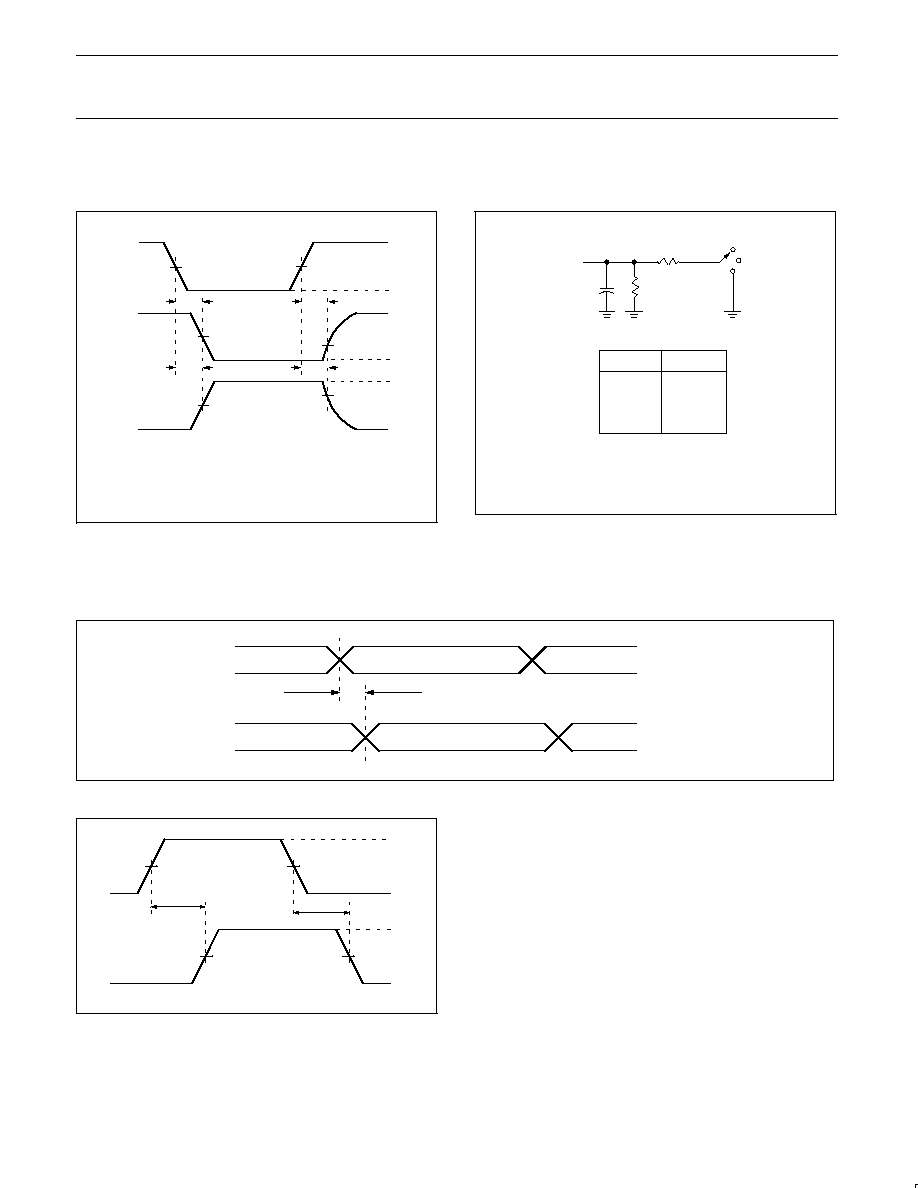
nDPx to HPx AC WAVEFORMS AND TEST CIRCUIT
AC WAVEFORM
Sn
(Low-level
enabling
1.25 V
t
PZH
t
PHZ
V
OH
V
OL
t
PZL
t
PLZ
2.5V
V
OL
V
OL
+ 0.3V
V
OH
0.3V
1.25 V
1.25 V
2.5 V
Output
HPx
SW at 4.3 V
(see Note 1)
Note:
1. The output is low except when disabled by the Sn control.
2. The output is high except when disabled by the Sn control.
Output
HPx
SW at Open
(see Note 2)
0 V
SA00623
1.25 V
Waveform 3. 3-State Output Enable and Disable Times
TEST CIRCUIT nDPx to HPx
2
×
V
CC
C
L
= 30 pF
500
Load Circuit
DEFINITIONS
C
L
=
Load capacitance includes jig and probe capacitance
TEST
SW
t
pd
open
t
PLZ
/t
PZL
2
×
V
CC
t
PHZ
/t
PZH
GND
500
From Output
Under Test
SW
Open
GND
SA00624
NOTES:
1. All input pulses are supplied by generators having the
following characteristics: PRR
10 MHz, Z
O
= 50
, t
r
2.5 ns,
t
f
2.5 ns.
2. The outputs are measured one at a time with one transition per
measurement.
skew
ANY TWO OUTPUTS
SW00396
Waveform 4. Skew Between Any Two Outputs
INPUT
1.25 V
OUTPUT
1.25 V
1.25 V
1.25 V
2.5 V
0 V
V
OH
V
OL
SA00568
RISING EDGE
SKEW
FALLING EDGE
SKEW
Waveform 5. Rising and Falling Edge Skew
Philips Semiconductors
Product data
CBTV4010
10-bit DDR SDRAM mux/bus switch
2002 Feb 19
8
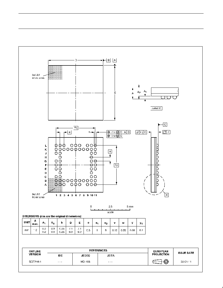
TFBGA64:
plastic thin fine-pitch ball grid array package; 64 balls; body 7 x 7 x 0.7 mm
SOT746-1

Philips Semiconductors
Product data
CBTV4010
10-bit DDR SDRAM mux/bus switch
2002 Feb 19
9
NOTES
Philips Semiconductors
Product data
CBTV4010
10-bit DDR SDRAM mux/bus switch
2002 Feb 19
10
Definitions
Short-form specification -- The data in a short-form specification is extracted from a full data sheet with the same type number and title. For
detailed information see the relevant data sheet or data handbook.
Limiting values definition -- Limiting values given are in accordance with the Absolute Maximum Rating System (IEC 60134). Stress above one
or more of the limiting values may cause permanent damage to the device. These are stress ratings only and operation of the device at these or
at any other conditions above those given in the Characteristics sections of the specification is not implied. Exposure to limiting values for extended
periods may affect device reliability.
Application information -- Applications that are described herein for any of these products are for illustrative purposes only. Philips
Semiconductors make no representation or warranty that such applications will be suitable for the specified use without further testing or
modification.
Disclaimers
Life support -- These products are not designed for use in life support appliances, devices or systems where malfunction of these products can
reasonably be expected to result in personal injury. Philips Semiconductors customers using or selling these products for use in such applications
do so at their own risk and agree to fully indemnify Philips Semiconductors for any damages resulting from such application.
Right to make changes -- Philips Semiconductors reserves the right to make changes, without notice, in the products, including circuits, standard
cells, and/or software, described or contained herein in order to improve design and/or performance. Philips Semiconductors assumes no
responsibility or liability for the use of any of these products, conveys no license or title under any patent, copyright, or mask work right to these
products, and makes no representations or warranties that these products are free from patent, copyright, or mask work right infringement, unless
otherwise specified.
Contact information
For additional information please visit
http://www.semiconductors.philips.com.
Fax: +31 40 27 24825
For sales offices addresses send e-mail to:
sales.addresses@www.semiconductors.philips.com.
©
Koninklijke Philips Electronics N.V. 2002
All rights reserved. Printed in U.S.A.
Date of release: 02-02
Document order number:
9397 750 09463
Philips
Semiconductors
Data sheet status
[1]
Objective data
Preliminary data
Product data
Product
status
[2]
Development
Qualification
Production
Definitions
This data sheet contains data from the objective specification for product development.
Philips Semiconductors reserves the right to change the specification in any manner without notice.
This data sheet contains data from the preliminary specification. Supplementary data will be
published at a later date. Philips Semiconductors reserves the right to change the specification
without notice, in order to improve the design and supply the best possible product.
This data sheet contains data from the product specification. Philips Semiconductors reserves the
right to make changes at any time in order to improve the design, manufacturing and supply.
Changes will be communicated according to the Customer Product/Process Change Notification
(CPCN) procedure SNW-SQ-650A.
Data sheet status
[1] Please consult the most recently issued data sheet before initiating or completing a design.
[2] The product status of the device(s) described in this data sheet may have changed since this data sheet was published. The latest information is available on the Internet at URL
http://www.semiconductors.philips.com.
Document Outline
- FEATURES
- QUICK REFERENCE DATA
- DESCRIPTION
- ORDERING INFORMATION
- 64-BALL BGA CONFIGURATION
- PIN DESCRIPTION
- FUNCTION TABLE
- ABSOLUTE MAXIMUM RATINGS
- RECOMMENDED OPERATING CONDITIONS
- DC ELECTRICAL CHARACTERISTICS
- AC CHARACTERISTICS
- AC WAVEFORMS
- AC WAVEFORM
- package
- Data sheet status
- Definitions