 | –≠–ª–µ–∫—Ç—Ä–æ–Ω–Ω—ã–π –∫–æ–º–ø–æ–Ω–µ–Ω—Ç: CGY2110CU | –°–∫–∞—á–∞—Ç—å:  PDF PDF  ZIP ZIP |
Document Outline
- FEATURES
- GENERAL DESCRIPTION
- APPLICATIONS
- ORDERING INFORMATION
- BLOCK DIAGRAM
- PINNING
- LIMITING VALUES
- ESD WARNING
- DC CHARACTERISTICS
- AC CHARACTERISTICS
- TEST AND APPLICATION INFORMATION
- BONDING PAD LOCATIONS
- DATA SHEET STATUS
- DEFINITIONS
- PACKAGE

DATA SHEET
Preliminary specification
File under Integrated Circuits, IC19
2001 Dec 07
INTEGRATED CIRCUITS
CGY2110CU
10 Gbits/s transimpedance
amplifier

2001 Dec 07
2
Philips Semiconductors
Preliminary specification
10 Gbits/s transimpedance amplifier
CGY2110CU
FEATURES
∑
Suitable for 10 Gbits/s optical fibre links
∑
Transimpedance gain 66 dB
(transimpedance 2 k
)
∑
Low noise <9 pA/
Hz
∑
Differential output
∑
Single 5.7 V power supply
∑
Low power consumption of 400 mW
∑
Supplied in bare die form.
APPLICATIONS
∑
Digital fibre optic receiver for optical
telecommunications (e.g. STM-64 or OC192 systems)
∑
High sensitivity and high gain amplifier.
GENERAL DESCRIPTION
The CGY2110CU is a 10 Gbits/s transimpedance
amplifier. Typical use is as a low noise preamplifier for light
wave receiver modules in optical fibre networks.
The CGY2110CU features differential outputs and
operates using a single 5.7 V supply voltage with a very
low power consumption of 400 mW (typical value).
The RF input and the photodiode biasing pad of the circuit
may be directly connected to a low capacitance
photodiode using short bond wires. A biasing circuit for the
photodiode is integrated on the CGY2110CU.
This GaAs Monolithic Microwave Integrated Circuit
(MMIC) was designed in cooperation with France Telecom
R&D and is fabricated using one of OMMIC's fully released
millimetre-wave GaAs Pseudomorphic High Electron
Mobility Transistor (PHEMT) processes.
This device is supplied as a RF tested bare die.
ORDERING INFORMATION
TYPE
NUMBER
PACKAGE
NAME
DESCRIPTION
VERSION
CGY2110CU
-
GaAs bare die
-

2001 Dec 07
3
Philips Semiconductors
Preliminary specification
10 Gbits/s transimpedance amplifier
CGY2110CU
BLOCK DIAGRAM
handbook, full pagewidth
MLD586
TRANSIMPEDANCE
AMPLIFIER
DIFFERENTIAL
AMPLIFIER
3.5 k
OUTN
13 SN
12
11 S
10
9
6
5
4
3
50
2
7
8
ST 1
INC
VPIN
Vbias
VS
VREF
VD3
VD
VDD
INA
Iphoto
SP
OUTP
Fig.1 Block diagram.
PINNING
LIMITING VALUES
In accordance with the Absolute Maximum Rating System (IEC 60134).
SYMBOL
PAD
DESCRIPTION
ST
1
do not bond
INA
2
photodiode (anode) input
INC
3
photodiode (cathode) biasing pad
VPIN
4
photodiode DC biasing voltage; optional use
VS
5
ground; bond to ground with lowest possible inductance
VREF
6
reference voltage pad; must be decoupled to ground using external capacitor(s)
VD
7
drain supply voltage (V
DD
)
VD3
8
drain supply voltage 3 (V
DD
)
SP
9
ground; bond to ground
OUTP
10
RF output
S
11
ground; bond to ground
OUTN
12
complementary RF output
SN
13
ground; bond to ground
SYMBOL
PARAMETER
MIN.
MAX.
UNIT
V
DD
supply voltage on pads VD and VD3
-
0.5
+8
V
V
bias
photodiode biasing voltage
-
15
+15
V
I
photo
input photodiode current
-
1
+2.5
mA
T
stg
storage temperature
-
55
+150
∞
C
T
ch(max)
maximum operating channel temperature
-
150
∞
C

2001 Dec 07
4
Philips Semiconductors
Preliminary specification
10 Gbits/s transimpedance amplifier
CGY2110CU
ESD WARNING
The CGY2110CU is a very high performance GaAs device and as such care must be taken at all times to avoid damage
by electrostatic discharge.
DC CHARACTERISTICS
V
DD
= 5.7 V; T
amb
= 25
∞
C; unless otherwise specified.
Note
1. As shown in Fig.1, the forward current is assumed to flow from the outside towards the inside of the device, whereas
the reverse current is assumed to flow from the inside towards the outside of the device.
AC CHARACTERISTICS
V
DD
= 5.7 V
±
5%; T
amb
= 25
∞
C; R
L
= 50
; unless otherwise specified; notes 1 and 2.
SYMBOL
PARAMETER
CONDITIONS
MIN.
TYP.
MAX.
UNIT
V
DD
supply voltage on pads VD
and VD3
5.4
5.7
6.0
V
I
DD
total supply current
40
70
100
mA
P
DC
DC power consumption
228
400
570
mW
I
photo(max)
maximum photodiode current
before input overload occurs; note 1
forward current
-
1.8
-
mA
reverse current
-
0.3
-
mA
V
O
DC voltage difference between
pads OUTP and OUTN
-
0.7
-
+0.7
V
T
amb
ambient temperature
operating
-
10
-
+85
∞
C
SYMBOL
PARAMETER
CONDITIONS
MIN.
TYP.
MAX.
UNIT
Z
tr
LF
low-frequency transimpedance
gain
f = 100 MHz
single-ended output
62
66
70
dB
differential output
-
72
-
dB
Z
tr
transimpedance gain ripple
Z
tr
=
Z
tr
-
Z
tr
LF
; see Fig.2
f = 1 MHz to 3 GHz
-
1.5
0
+1.5
dB
f = 3 to 6 GHz
-
1.5
+1
+3
dB
f = 6 to 10 GHz
-
-
3
dB
f
co
transimpedance cut-off
frequency
Z
tr
=
Z
tr
LF
-
3 dB
C
p
= 0.22 pF
8
9
-
GHz
C
p
= 0.14 pF
-
10.1
-
GHz
t
d(g)
group delay
relative to f = 2.5 GHz; see Fig.3
f = 1 to 3 GHz
-
20
-
+20
ps
f = 4 GHz
-
10
-
+35
ps
f = 5 GHz
0
-
50
ps
f = 6.5 to 9 GHz
15
-
75
ps
s
22
output reflection coefficient
f = 100 MHz to 10 GHz; note 3
-
-
15
-
10
dB

2001 Dec 07
5
Philips Semiconductors
Preliminary specification
10 Gbits/s transimpedance amplifier
CGY2110CU
Notes
1. Photodiode and input-parasitics model: C
p
= 0.22 pF; R
s
= 8
;
-
3 dB intrinsic optical cut-off frequency = 15 GHz;
L
b
= 0.6 nH (where L
b
= L
ba
+ L
bc
); see Fig.5.
2. AC characteristics are guaranteed for pad OUTP (with pad OUTN loaded by 50
via a DC decoupling capacitor).
3. The
s
22
specification given in this table is based on RF on-wafer measurements with low-inductance probes. It is
recommended that ground and output bonding wires are kept as short as possible so as not to degrade this
parameter (see also "Test and application information").
I
n(i)(eq)
equivalent input noise current
density
f = 1 to 4 GHz; C
p
= 0.22 pF
-
4.7
7
pA/
Hz
f = 7 GHz; C
p
= 0.22 pF
-
6.5
10
pA/
Hz
f = 10 GHz; C
p
= 0.14 pF
-
8
-
pA/
Hz
I
n(i)(tot)(rms)
total integrated input noise
current (RMS value)
f = 10 MHz to 8 GHz; C
p
= 0.22 pF
-
450
650
nA
f = 10 MHz to 10 GHz; C
p
= 0.14 pF
-
500
-
nA
R
L
output load resistance
pads OUTN and OUTP
-
50
-
SYMBOL
PARAMETER
CONDITIONS
MIN.
TYP.
MAX.
UNIT
handbook, halfpage
0
2
f (GHz)
10
4
2
-
2
-
4
0
4
6
8
MLD566
Ztr
(dB)
Fig.2
Transimpedance gain ripple as a function of
the frequency.
Hatched area indicates limit of test specification.
handbook, halfpage
80
-
40
0
40
MLD567
0
2
f (GHz)
10
4
6
8
td(g)
(ps)
Fig.3 Group delay as a function of the frequency.
Hatched area indicates limit of test specification.

2001 Dec 07
6
Philips Semiconductors
Preliminary specification
10 Gbits/s transimpedance amplifier
CGY2110CU
TEST AND APPLICATION INFORMATION
Typical application scheme
A typical receiver module, including a photodiode and a
CGY2110CU transimpedance amplifier is shown in Fig.4
and the electrical equivalent model of the module is shown
in Fig.5.
To ensure the best performance of the receiver module,
the shortest possible connection between photodiode and
the IC must be used for both input pads INA and INC.
The same precaution applies to the output pads OUTN
and OUTP, where the bonding wires should be as short as
possible. Pad VS should also be connected to ground with
the shortest possible bonding wire.
Pad VREF is decoupled directly to ground while pads VD3
and VD are decoupled and connected to the V
DD
power
supply.
A high-value resistor R
bias
is put in series with pad VPIN to
protect the photodiode against high currents in the event
of high illumination. The value of R
bias
is determined by the
photodiode characteristics. The recommended decoupling
scheme uses a high-frequency ceramic capacitor of 50 pF
(typical value) placed close to the IC and a low-frequency
multilayer capacitor placed at greater distance. The value
of C
ref
is determined by the required low-frequency cut-off
point, given by the time constant of the RC circuit
(capacitor C
ref
and a 3500
on-chip resistor).
handbook, full pagewidth
Cref
Rbias
Vbias
VDD
OUTN
OUTP
(1)
(1)
(2)
ground
plane
photodiode
(2)
CGY2110CU
MLD568
Fig.4 Module layout for a typical application.
(1) Low frequency decoupling capacitor.
(2) High frequency decoupling capacitor.

2001 Dec 07
7
Philips Semiconductors
Preliminary specification
10 Gbits/s transimpedance amplifier
CGY2110CU
handbook, full pagewidth
50
line
50
line
RL =
50
output (N)
Cp
(1)
Rs
Lba
Lbc
output (P)
CGY2110CU
MLD569
(1) Photodiode equivalent circuit.
Fig.5 Electrical equivalent model of the module.
Operating conditions of photodiode
The performance of the photodiode receiver module is
very dependent on both the photodiode capacitance and
the interconnection inductance between the photodiode
and the CGY2110CU. The circuit was optimized for a
photodiode capacitance C
p
equal (or lower) than 0.22 pF
with a low photodiode series resistance R
s
to give the best
noise performance from the receiver module.
It is strongly recommended to use short bondings between
the photodiode and the CGY2110CU, in order to keep the
bonding inductances L
ba
and L
bc
to respectively the signal
inputs INA and INC as low as possible. A total equivalent
inductance L
b
of 0.6 nH is recommended while 1.0 nH
should be considered a maximum value.
Typical results (computed measurements)
The s-parameters of the CGY2110CU are measured
on-wafer under nominal conditions, using 40 GHz
bandwidth probes. These s-parameters may then be used
with the photodiode parameters in order to simulate the
complete 10 Gbits/s receiver module performance
(photodiode plus CGY2110CU).
The transimpedance gain and the equivalent input noise
current of receiver modules using the CGY2110CU are
thus drawn for various photodiode parameter values in
Figs 6 to 13. The photodiode
-
3 dB intrinsinc optical
cut-off frequency is always assumed to be 15 GHz. The
values of C
p
, L
b
and R
s
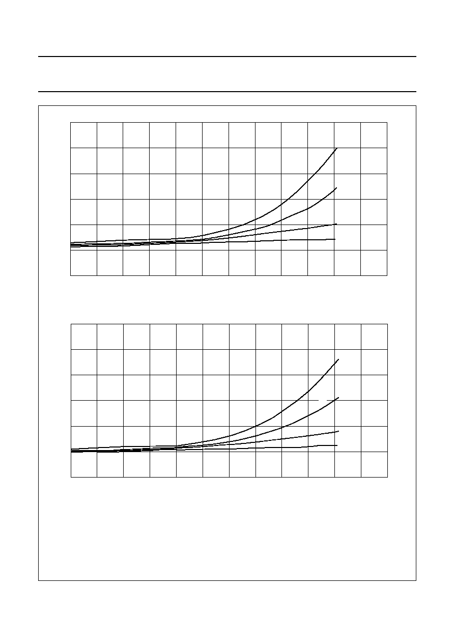
are defined as in Fig.5.
From Figs 6 and 7, it is clear that the lowest possible
photodiode capacitance C
p
will lead to the lowest noise,
while Figs 8 and 9 show that the lowest possible bonding
inductance value L
b
will lead to the flattest gain response.
Recommended values are C
p
< 0.25 pF and L
b
< 0.6 nH.
Figures 10 to 13 show the variation of the transimpedance
gain, equivalent input noise current, group delay and
output matching (s
22
) as a function of the temperature and
the supply voltage.
2001 Dec 07
8
Philips Semiconductors
Preliminary specification
10 Gbits/s transimpedance amplifier
CGY2110CU
handbook, full pagewidth
12
10
12
9
6
3
0
2
4
6
8
MLD570
f (GHz)
In(i)eq
(pA/
Hz)
(1)
(2)
(3)
(4)
handbook, full pagewidth
12
10
12
9
6
3
0
2
4
6
8
MLD571
f (GHz)
In(i)eq
(pA/
Hz)
(1)
(3)
(4)
(2)
b. V
DD
= 6.0 V.
a. V
DD
= 5.4 V.
Fig.6
Equivalent input noise current density as a function of the frequency with different values of the internal
photodiode capacitance.
R
s
= 8
; L
b
= 0.6 nH.
(1) C
p
= 0.22 pF.
(2) C
p
= 0.18 pF.
(3) C
p
= 0.14 pF.
(4) C
p
= 0.10 pF.
2001 Dec 07
9
Philips Semiconductors
Preliminary specification
10 Gbits/s transimpedance amplifier
CGY2110CU
handbook, full pagewidth
12
10
12
9
6
3
0
2
4
6
8
MLD572
f (GHz)
In(i)eq
(pA/
Hz)
(1)
(3)
(4)
(2)
handbook, full pagewidth
12
10
12
9
6
3
0
2
4
6
8
MLD573
f (GHz)
In(i)eq
(pA/
Hz)
(1)
(3)
(4)
(2)
Fig.7
Equivalent input noise current density as a function of the frequency with different values of the bonding
inductance to the photodiode.
R
s
= 8
; C
p
= 0.22 pF.
(1) L
b
= 2
◊
0.7 nH.
(2) L
b
= 2
◊
0.5 nH.
(3) L
b
= 2
◊
0.3 nH.
(4) L
b
= 2
◊
0.1 nH.
b. V
DD
= 6.0 V.
a. V
DD
= 5.4 V.

2001 Dec 07
10
Philips Semiconductors
Preliminary specification
10 Gbits/s transimpedance amplifier
CGY2110CU
handbook, full pagewidth
12
10
70
68
66
64
62
0
2
4
6
8
MLD574
f (GHz)
Ztr
(dB
)
(1)
(2)
(3)
(4)
handbook, full pagewidth
12
10
70
68
66
64
62
0
2
4
6
8
MLD575
f (GHz)
Ztr
(dB
)
(1)
(2)
(4)
(3)
b. V
DD
= 6.0 V.
a. V
DD
= 5.4 V.
Fig.8
Transimpedance gain as a function of the frequency with different values of the internal photodiode
capacitance.
R
s
= 8
; L
b
= 0.6 nH.
(1) C
p
= 0.10 pF.
(2) C
p
= 0.14 pF.
(3) C
p
= 0.18 pF.
(4) C
p
= 0.22 pF.

2001 Dec 07
11
Philips Semiconductors
Preliminary specification
10 Gbits/s transimpedance amplifier
CGY2110CU
handbook, full pagewidth
12
10
70
68
66
64
62
0
2
4
6
8
MLD576
f (GHz)
Ztr
(dB
)
(1)
(2)
(4)
(3)
handbook, full pagewidth
12
10
70
68
66
64
62
0
2
4
6
8
MLD577
f (GHz)
Ztr
(dB
)
(1)
(2)
(4)
(3)
R
s
= 8
; C
p
= 0.22 pF.
(1) L
b
= 2
◊
0.7 nH.
(2) L
b
= 2
◊
0.5 nH.
(3) L
b
= 2
◊
0.3 nH.
(4) L
b
= 2
◊
0.1 nH.
b. V
DD
= 6.0 V.
a. V
DD
= 5.4 V.
Fig.9
Transimpedance gain as a function of the frequency with different values of the bonding inductance to the
photodiode.

2001 Dec 07
12
Philips Semiconductors
Preliminary specification
10 Gbits/s transimpedance amplifier
CGY2110CU
handbook, full pagewidth
10
2
0
-
2
-
4
0
2
4
6
8
MLD578
(1)
(3)
(2)
f (GHz)
Ztr
(dB)
(4)
handbook, full pagewidth
10
2
0
-
2
-
4
0
2
4
6
8
MLD579
(1)
(2)
f (GHz)
Ztr
(dB)
(4)
(3)
b. V
DD
= 6.0 V.
a. V
DD
= 5.4 V.
Fig.10 Transimpedance gain ripple as a function of the frequency with different values of the operating
temperature.
R
s
= 8
; C
p
= 0.22 pF; L
b
= 0.6 nH.
(1) T
amb
= 25
∞
C.
(2) T
amb
= 50
∞
C.
(3) T
amb
= 75
∞
C.
(4) T
amb
= 100
∞
C.
2001 Dec 07
13
Philips Semiconductors
Preliminary specification
10 Gbits/s transimpedance amplifier
CGY2110CU
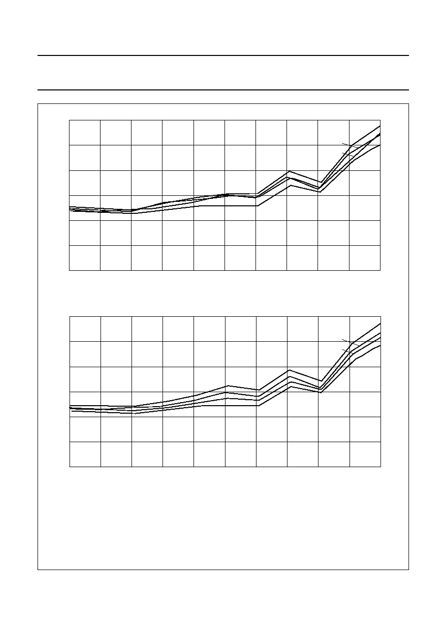
handbook, full pagewidth
10
12
8
4
0
0
2
4
6
8
MLD580
(1)
(2)
(3)
f (GHz)
In(i)eq
(pA/
Hz)
(4)
handbook, full pagewidth
10
12
8
4
0
0
2
4
6
8
MLD581
f (GHz)
In(i)eq
(pA/
Hz)
(1)
(2)
(3)
(4)
b. V
DD
= 6.0 V.
Fig.11 Equivalent input noise current density as a function of the frequency with different values of the operating
temperature.
a. V
DD
= 5.4 V.
R
s
= 8
; C
p
= 0.22 pF; L
b
= 0.6 nH.
(1) T
amb
= 100
∞
C.
(2) T
amb
= 75
∞
C.
(3) T
amb
= 50
∞
C.
(4) T
amb
= 25
∞
C.

2001 Dec 07
14
Philips Semiconductors
Preliminary specification
10 Gbits/s transimpedance amplifier
CGY2110CU
handbook, full pagewidth
10
80
-
20
0
2
4
6
8
0
20
40
60
MLD582
(1)
(2)
td(g)
(ps)
(4)
(3)
f (GHz)
handbook, full pagewidth
10
80
-
20
0
2
4
6
8
0
20
40
60
MLD583
(1)
(2)
td(g)
(ps)
(4)
(3)
f (GHz)
b. V
DD
= 6.0 V.
Fig.12 Group delay (relative to f = 2.5 GHz) as a function of the frequency with different values of the operating
temperature.
R
s
= 8
; C
p
= 0.22 pF; L
b
= 0.6 nH.
(1) T
amb
= 25
∞
C.
(2) T
amb
= 50
∞
C.
(3) T
amb
= 75
∞
C.
(4) T
amb
= 100
∞
C.
a. V
DD
= 5.4 V.

2001 Dec 07
15
Philips Semiconductors
Preliminary specification
10 Gbits/s transimpedance amplifier
CGY2110CU
handbook, full pagewidth
10
-
10
-
20
-
30
-
40
0
2
4
6
8
MLD584
f (GHz)
s22
(dB)
(1)
(2)
(3)
(4)
handbook, full pagewidth
10
-
10
-
20
-
30
-
40
0
2
4
6
8
MLD585
f (GHz)
s22
(dB)
(1)
(2)
(3)
(4)
a. V
DD
= 5.4 V.
Fig.13 Output reflection coefficient as a function of the frequency with different values of the operating
temperature.
b. V
DD
= 6.0 V.
R
s
= 8
; C
p
= 0.22 pF; L
b
= 0.6 nH.
(1) T
amb
= 100
∞
C.
(2) T
amb
= 75
∞
C.
(3) T
amb
= 50
∞
C.
(4) T
amb
= 25
∞
C.
2001 Dec 07
16
Philips Semiconductors
Preliminary specification
10 Gbits/s transimpedance amplifier
CGY2110CU
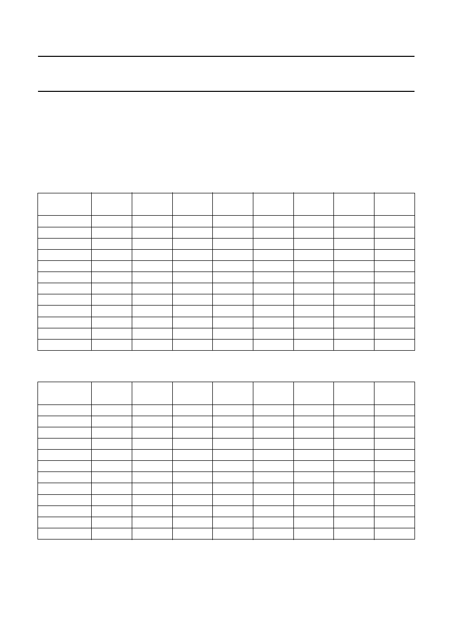
s-parameter data
The s-parameters of the CGY2110CU die are measured on-wafer using 40 GHz bandwidth probes.
Port 1 is the input (INA), while port 2 is the output (OUTP). For these measurements pad OUTN is connected to a 50
load via a DC blocking capacitor.
Measurement data from a typical CGY2110CU chip are shown in Tables 1 and 2.
Table 1
Measured s-parameters of the CGY2110CU at V
DD
= 5.4 V
Test conditions: R
L
= 50
; T
amb
= 25
∞
C; magnitude is given in dB and phase is given in degrees.
Table 2
Measured s-parameters of the CGY2110CU at V
DD
= 6.0 V
Test conditions: R
L
= 50
; T
amb
= 25
∞
C; magnitude is given in dB and phase is given in degrees.
FREQUENCY
(GHz)
s
11
s
11
s
12
s
12
s
21
s
21
s
22
s
22
0.1
-
5.04
-
1.17
-
72.3
-
3
+25.87
-
1.5
-
53
+152
1.1
-
6.02
-
11.8
-
66.0
-
112
+27.44
-
19.7
-
15.1
+47.2
2.1
-
7.38
-
15.9
-
69.2
+176
+29.21
-
49.3
-
23.2
-
35.6
3.1
-
9.32
-
16.6
-
62.5
-
35
+30.48
-
84.8
-
18.3
-
3.37
4.1
-
11.1
-
7.0
-
64.2
-
165
+31.29
-
124
-
22.8
-
65
5.1
-
12
+9.0
-
71.4
+137
+31.77
-
164
-
27.4
-
66.9
6.1
-
10.6
+24.7
-
82.5
-
115
+31.65
+156
-
35.4
-
178
7.1
-
9.19
+31.9
-
68.1
-
129
+31.32
+112
-
21.8
+136
8.1
-
7.7
+35.1
-
66.8
+179
+30.14
+64.3
-
14.4
+72.1
8.7
-
6.86
+35.7
-
67.0
-
158
+28.84
+37.6
-
14.7
+44.0
9.1
-
6.45
+35.0
-
62.8
-
162
+27.58
+20.2
-
17.0
+31.4
10.1
-
5.08
+34.5
-
59.4
-
173
+24.52
-
15.4
-
13.4
+40.3
FREQUENCY
(GHz)
s
11
s
11
s
12
s
12
s
21
s
21
s
22
s
22
0.1
-
5.57
-
0.78
-
79.5
+103
+27.17
-
1.5
-
61.2
+107
1.1
-
6.54
-
10.5
-
65.9
-
99
+28.65
-
20.1
-
14.4
+48.3
2.1
-
7.84
-
14.1
-
69.6
+138
+30.24
-
49.4
-
24.1
-
46.2
3.1
-
9.52
-
11.9
-
62.3
-
28
+31.44
-
83.6
-
17.7
+1.8
4.1
-
11
-
3.46
-
63.8
-
167
+32.27
-
121
-
22.1
-
62.7
5.1
-
11.7
+13
-
69.9
+145
+32.89
-
160
-
25.6
-
65.2
6.1
-
10.2
+25.9
-
78.7
-
154
+32.90
+161
-
32.9
-
163
7.1
-
8.85
+31.2
-
70.2
-
138
+32.89
+119
-
20.9
+145
8.1
-
7.51
+33.8
-
68.5
-
173
+32.23
+70.7
-
13.2
+80.3
8.7
-
6.77
+34.2
-
67.8
-
161
+31.08
+42.4
-
13.5
+50.4
9.1
-
6.29
+34.1
-
61.8
-
165
+29.82
+24.0
-
16.1
+36.7
10.1
-
5.01
+33.7
-
60.1
-
177
+26.71
-
13.2
-
11.9
+46.2

2001 Dec 07
17
Philips Semiconductors
Preliminary specification
10 Gbits/s transimpedance amplifier
CGY2110CU
BONDING PAD LOCATIONS
Note
1. All x and y coordinates in
µ
m represent the position of the centre of the pad with respect to the left bottom corner
(see Fig.14).
SYMBOL
PAD
COORDINATES
(1)
x
y
ST
1
110
540
INA
2
110
390
INC
3
110
240
VPIN
4
240
110
VS
5
390
110
VREF
6
540
110
VD
7
690
110
VD3
8
840
110
SP
9
1035
110
OUTP
10
1090
265
S
11
1090
390
OUTN
12
1090
515
SN
13
1090
660
handbook, full pagewidth
60
µ
m
85
µ
m
120
µ
m
125
µ
m
125
µ
m
265
µ
m
240
µ
m
240
µ
m
240
µ
m
150
µ
m
150
µ
m
150
µ
m
150
µ
m
150
µ
m
150
µ
m
100
µ
m
190
µ
m
60
µ
m
11
780
±
15
µ
m
1190
±
15
µ
m
12
13
10
9
8
7
1
2
3
6
5
4
SN
VPIN
VS
SP
VD
VD3
OUTN
S
OUTP
VREF
ST
INR
INC
CGY2110
R1883 -2d
MLD565
Fig.14 Bonding pad locations.

2001 Dec 07
18
Philips Semiconductors
Preliminary specification
10 Gbits/s transimpedance amplifier
CGY2110CU
Table 3
Physical characteristics of bare die
PARAMETER
VALUE
Size
1190
±
15
µ
m
◊
780
±
15
µ
m
Thickness
200
µ
m
Backside material
TiAu
Glass passivation
SiN
Bonding pad dimensions
VPIN, VS, VREF, VD and VD3
100
◊
100
µ
m
SP
190
◊
100
µ
m
OUTP, OUTN and S
100
◊
80
µ
m
SN
270
◊
100
µ
m
ST and INC
100
◊
120
µ
m
INA
80
◊
80
µ
m
Attach temperature
<135
∞
C
Attach time
<15 s

2001 Dec 07
19
Philips Semiconductors
Preliminary specification
10 Gbits/s transimpedance amplifier
CGY2110CU
DATA SHEET STATUS
Notes
1. Please consult the most recently issued data sheet before initiating or completing a design.
2. The product status of the device(s) described in this data sheet may have changed since this data sheet was
published. The latest information is available on the Internet at URL http://www.semiconductors.philips.com.
DATA SHEET STATUS
(1)
PRODUCT
STATUS
(2)
DEFINITIONS
Objective data
Development
This data sheet contains data from the objective specification for product
development. Philips Semiconductors reserves the right to change the
specification in any manner without notice.
Preliminary data
Qualification
This data sheet contains data from the preliminary specification.
Supplementary data will be published at a later date. Philips
Semiconductors reserves the right to change the specification without
notice, in order to improve the design and supply the best possible
product.
Product data
Production
This data sheet contains data from the product specification. Philips
Semiconductors reserves the right to make changes at any time in order
to improve the design, manufacturing and supply. Changes will be
communicated according to the Customer Product/Process Change
Notification (CPCN) procedure SNW-SQ-650A.
DEFINITIONS
Short-form specification
The data in a short-form
specification is extracted from a full data sheet with the
same type number and title. For detailed information see
the relevant data sheet or data handbook.
Limiting values definition
Limiting values given are in
accordance with the Absolute Maximum Rating System
(IEC 60134). Stress above one or more of the limiting
values may cause permanent damage to the device.
These are stress ratings only and operation of the device
at these or at any other conditions above those given in the
Characteristics sections of the specification is not implied.
Exposure to limiting values for extended periods may
affect device reliability.
Application information
Applications that are
described herein for any of these products are for
illustrative purposes only. Philips Semiconductors make
no representation or warranty that such applications will be
suitable for the specified use without further testing or
modification.
DISCLAIMERS
Life support applications
These products are not
designed for use in life support appliances, devices, or
systems where malfunction of these products can
reasonably be expected to result in personal injury. Philips
Semiconductors customers using or selling these products
for use in such applications do so at their own risk and
agree to fully indemnify Philips Semiconductors for any
damages resulting from such application.
Right to make changes
Philips Semiconductors
reserves the right to make changes, without notice, in the
products, including circuits, standard cells, and/or
software, described or contained herein in order to
improve design and/or performance. Philips
Semiconductors assumes no responsibility or liability for
the use of any of these products, conveys no licence or title
under any patent, copyright, or mask work right to these
products, and makes no representations or warranties that
these products are free from patent, copyright, or mask
work right infringement, unless otherwise specified.
Bare die
All die are tested and are guaranteed to
comply with all data sheet limits up to the point of wafer
sawing for a period of ninety (90) days from the date of
Philips' delivery. If there are data sheet limits not
guaranteed, these will be separately indicated in the data
sheet. There are no post packing tests performed on
individual die or wafer. Philips Semiconductors has no
control of third party procedures in the sawing, handling,
packing or assembly of the die. Accordingly, Philips
Semiconductors assumes no liability for device
functionality or performance of the die or systems after
third party sawing, handling, packing or assembly of the
die. It is the responsibility of the customer to test and
qualify their application in which the die is used.

© Koninklijke Philips Electronics N.V. 2001
SCA73
All rights are reserved. Reproduction in whole or in part is prohibited without the prior written consent of the copyright owner.
The information presented in this document does not form part of any quotation or contract, is believed to be accurate and reliable and may be changed
without notice. No liability will be accepted by the publisher for any consequence of its use. Publication thereof does not convey nor imply any license
under patent- or other industrial or intellectual property rights.
Philips Semiconductors ≠ a worldwide company
Contact information
For additional information please visit http://www.semiconductors.philips.com.
Fax: +31 40 27 24825
For sales offices addresses send e-mail to: sales.addresses@www.semiconductors.philips.com.
Printed in The Netherlands
403510/01/pp
20
Date of release:
2001 Dec 07
Document order number:
9397 750 07776