DATA SHEET
Product specification
File under Integrated Circuits, IC04
January 1995
INTEGRATED CIRCUITS
HEF4014B
MSI
8-bit static shift register
For a complete data sheet, please also download:
∑
The IC04 LOCMOS HE4000B Logic
Family Specifications HEF, HEC
∑
The IC04 LOCMOS HE4000B Logic
Package Outlines/Information HEF, HEC

January 1995
2
Philips Semiconductors
Product specification
8-bit static shift register
HEF4014B
MSI
DESCRIPTION
The HEF4014B is a fully synchronous edge-triggered 8-bit
static shift register with eight synchronous parallel inputs
(P
0
to P
7
), a synchronous serial data input (D
S
), a
synchronous parallel enable input (PE), a LOW to HIGH
edge-triggered clock input (CP) and buffered parallel
outputs from the last three stages (O
5
to O
7
).
Operation is synchronous and the device is edge-triggered
on the LOW to HIGH transition of CP. Each register stage
is of a D-type master-slave flip-flop. When PE is HIGH,
data is loaded into the register from P
0
to P
7
on the LOW
to HIGH transition of CP. When PE is LOW, data is shifted
to the first position from D
S
, and all the data in the register
is shifted one position to the right on the LOW to HIGH
transition of CP. Schmitt-trigger action in the clock input
makes the circuit highly tolerant to slower clock rise and
fall times
Fig.1 Functional diagram.
Fig.2 Pinning diagram.
FAMILY DATA, I
DD
LIMITS category MSI
See Family Specifications
HEF4014BP(N):
16-lead DIL; plastic
(SOT38-1)
HEF4014BD(F):
16-lead DIL; ceramic (cerdip)
(SOT74)
HEF4014BT(D):
16-lead SO; plastic
(SOT109-1)
( ): Package Designator North America
January 1995
4
Philips Semiconductors
Product specification
8-bit static shift register
HEF4014B
MSI
PINNING
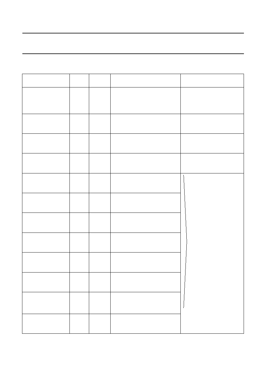
FUNCTION TABLES
Serial operation
PE
parallel enable input
P
0
to P
7
parallel data inputs
D
S
serial data input
CP
clock input (LOW to HIGH edge-triggered)
O
5
to O
7
buffered parallel outputs from the last three
stages
n
INPUTS
OUTPUTS
CP
D
S
PE
O
5
O
6
O
7
1
D
1
L
X
X
X
2
D
2
L
X
X
X
3
D
3
L
X
X
X
6
X
L
D
1
X
X
7
X
L
D
2
D
1
X
8
X
L
D
3
D
2
D
1
X
X
no change
Parallel operation
Notes
1. H = HIGH state (the more positive voltage)
L = LOW state (the less positive voltage)
X = state is immaterial
= positive-going transition
= negative-going transition
D
n
= either HIGH or LOW
n = number of clock pulse transitions
n
INPUTS
OUTPUTS
CP
D
S
PE
O
5
O
6
O
7
1
X
H
P
5
P
6
P
7
X
X
no change
AC CHARACTERISTICS
V
SS
= 0 V; T
amb
= 25
∞
C; C
L
= 50 pF; input transition times
20 ns
V
DD
V
TYPICAL FORMULA FOR P (
µ
W)
Dynamic power
5
900 f
i
+
(f
o
C
L
)
◊
V
DD
2
where
dissipation per
10
4 300 f
i
+
(f
o
C
L
)
◊
V
DD
2
f
i
= input freq. (MHz)
package (P)
15
12 000 f
i
+
(f
o
C
L
)
◊
V
DD
2
f
o
= output freq. (MHz)
C
L
= load cap. (pF)
(f
o
C
L
) = sum of outputs
V
DD
= supply voltage (V)