DATA SHEET
Product specification
File under Integrated Circuits, IC04
January 1995
INTEGRATED CIRCUITS
HEF4516B
MSI
Binary up/down counter
For a complete data sheet, please also download:
·
The IC04 LOCMOS HE4000B Logic
Family Specifications HEF, HEC
·
The IC04 LOCMOS HE4000B Logic
Package Outlines/Information HEF, HEC
January 1995
2
Philips Semiconductors
Product specification
Binary up/down counter
HEF4516B
MSI
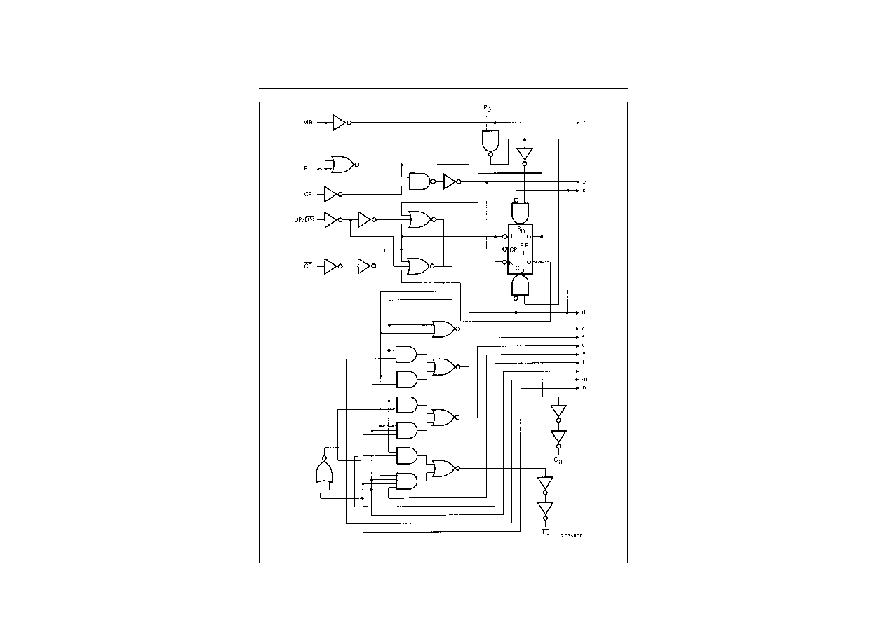
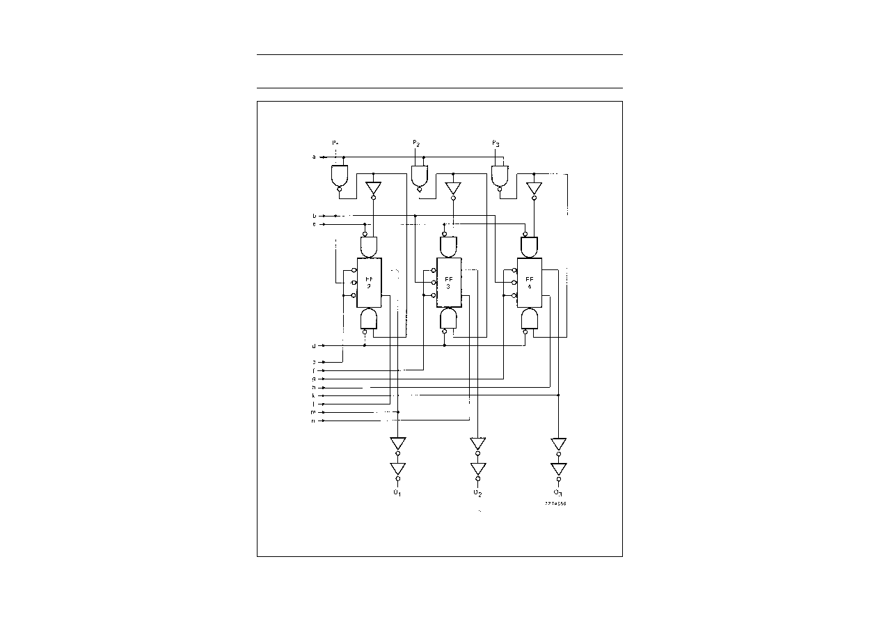
DESCRIPTION
The HEF4516B is an edge-triggered synchronous
up/down 4-bit binary counter with a clock input (CP), an
up/down count control input (UP/DN), an active LOW
count enable input (CE), an asynchronous active HIGH
parallel load input (PL), four parallel inputs (P
0
to P
3
), four
parallel outputs (O
0
to O
3
), an active LOW terminal count
output (TC), and an overriding asynchronous master reset
input (MR).
Information on P
0
to P
3
is loaded into the counter while PL
is HIGH, independent of all other input conditions except
MR which must be LOW. When PL and CE are LOW, the
counter changes on the LOW to HIGH transition of CP.
Input UP/DN determines the direction of the count, HIGH
for counting up, LOW for counting down. When counting
up, TC is LOW when O
0
and O
3
are HIGH and CE is LOW.
When counting down, TC is LOW when O
0
to O
3
and
CE are LOW. A HIGH on MR resets the counter (O
0
to
O
3
= LOW) independent of all other input conditions.
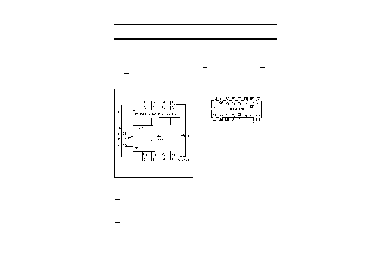
Fig.1 Functional diagram.
HEF4516BP(N):
16-lead DIL; plastic (SOT38-1)
HEF4516BD(F):
16-lead DIL; ceramic (cerdip) (SOT74)
HEF4516BT(D):
16-lead SO; plastic (SOT109-1)
( ): Package Designator North America
Fig.2 Pinning diagram.
PINNING
FAMILY DATA, I
DD
LIMITS category MSI
See Family Specifications
PL
parallel load input (active HIGH)
P
0
to P
3
parallel inputs
CE
count enable input (active LOW)
CP
clock pulse input (LOW to HIGH,
edge triggered)
UP/DN
up/down count control input
MR
master reset input
TC
terminal count output (active LOW)
O
0
to O
3
parallel outputs
January 1995
5
Philips Semiconductors
Product specification
Binary up/down counter
HEF4516B
MSI
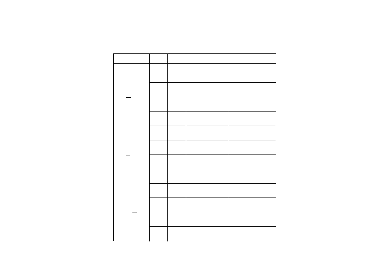
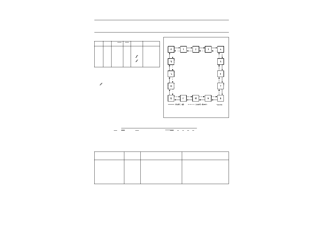
FUNCTION TABLE
Notes
1. H = HIGH state (the more positive voltage)
L = LOW state (the less positive voltage)
X = state is immaterial
= positive-going transition
MR
PL
UP/DN
CE
CP
MODE
L
H
X
X
X
parallel load
L
L
X
H
X
no change
L
L
L
L
count down
L
L
H
L
count up
H
X
X
X
X
reset
Fig.5 State diagram.
Logic equation for terminal count:
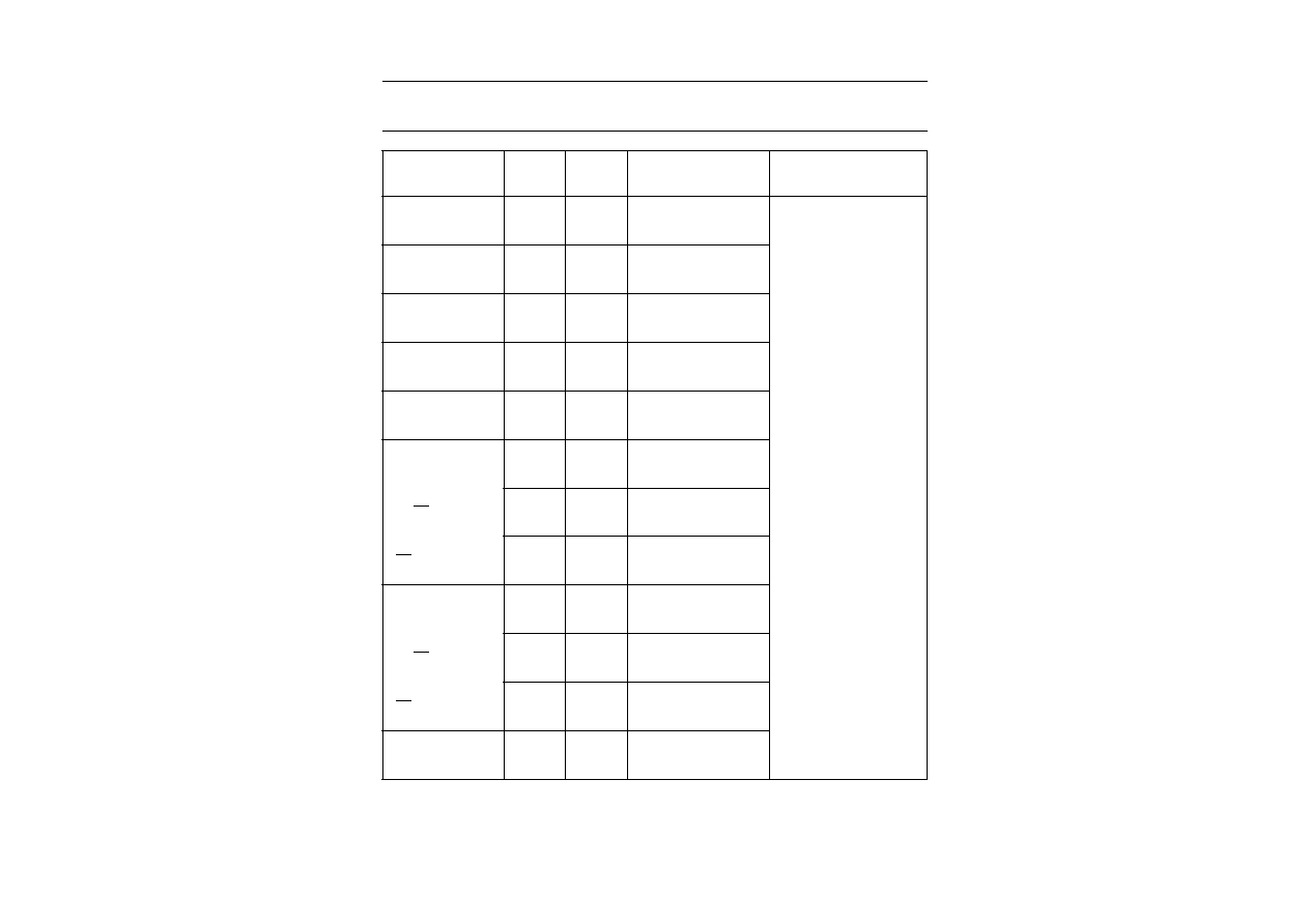
AC CHARACTERISTICS
V
SS
= 0 V; T
amb
= 25
°
C; input transition times
20 ns
V
DD
V
TYPICAL FORMULA FOR P (
µ
W)
Dynamic power
5
1000 f
i
+
(f
o
C
L
)
×
V
DD
2
where
dissipation per
10
4500 f
i
+
(f
o
C
L
)
×
V
DD
2
f
i
= input freq. (MHz)
package (P)
15
11 200 f
i
+
(f
o
C
L
)
×
V
DD
2
f
o
= output freq. (MHz)
C
L
= load capacitance (pF)
(f
o
C
L
) = sum of outputs
V
DD
= supply voltage (V)
TC
CE
UP/DN
(
)
O
0
O
1
O
2
O
3
UP/DN
O
0
O
1
O
2
O
3
+
{
}
=
January 1995
10
Philips Semiconductors
Product specification
Binary up/down counter
HEF4516B
MSI
This text is here in white to force landscape pages to be rotated correctly when browsing through the pdf in the Acrobat reader.This text is here in
_
white to force landscape pages to be rotated correctly when browsing through the pdf in the Acrobat reader.This text is here inThis text is here in
white to force landscape pages to be rotated correctly when browsing through the pdf in the Acrobat reader. white to force landscape pages to be ...
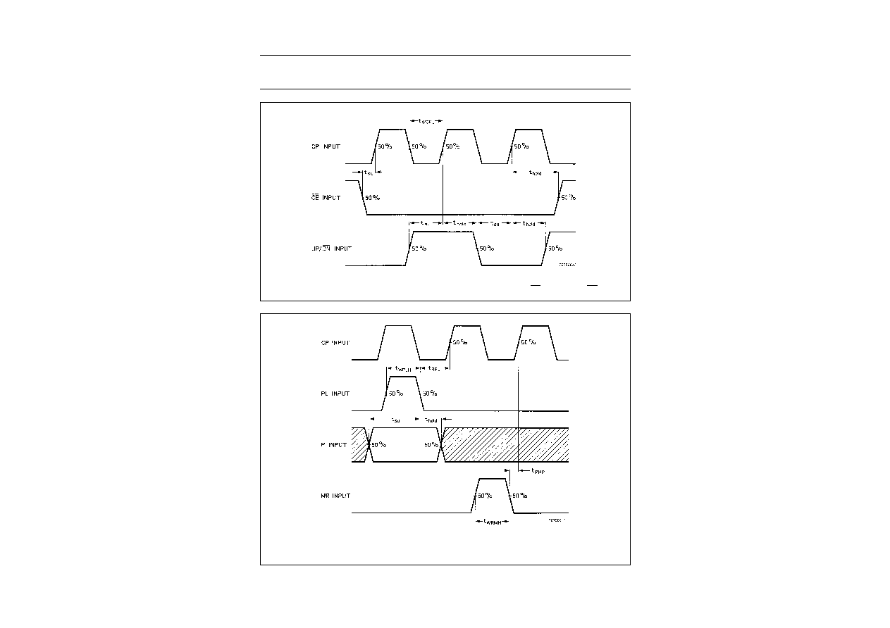
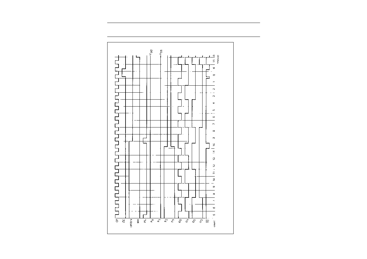
Fig.8 Timing diagram.