 | –≠–ª–µ–∫—Ç—Ä–æ–Ω–Ω—ã–π –∫–æ–º–ø–æ–Ω–µ–Ω—Ç: IRF540 | –°–∫–∞—á–∞—Ç—å:  PDF PDF  ZIP ZIP |

Philips Semiconductors
Product specification
N-channel TrenchMOS
TM
transistor
IRF540, IRF540S
FEATURES
SYMBOL
QUICK REFERENCE DATA
∑ 'Trench' technology
∑ Low on-state resistance
V
DSS
= 100 V
∑ Fast switching
∑ Low thermal resistance
I
D
= 23 A
R
DS(ON)
77 m
GENERAL DESCRIPTION
N-channel enhancement mode field-effect power transistor in a plastic envelope using 'trench' technology.
Applications:-
∑ d.c. to d.c. converters
∑ switched mode power supplies
∑ T.V. and computer monitor power supplies
The IRF540 is supplied in the SOT78 (TO220AB) conventional leaded package.
The IRF540S is supplied in the SOT404 (D
2
PAK) surface mounting package.
PINNING
SOT78 (TO220AB)
SOT404 (D
2
PAK)
PIN
DESCRIPTION
1
gate
2
drain
1
3
source
tab
drain
LIMITING VALUES
Limiting values in accordance with the Absolute Maximum System (IEC 134)
SYMBOL PARAMETER
CONDITIONS
MIN.
MAX.
UNIT
V
DSS
Drain-source voltage
T
j
= 25 ∞C to 175∞C
-
100
V
V
DGR
Drain-gate voltage
T
j
= 25 ∞C to 175∞C; R
GS
= 20 k
-
100
V
V
GS
Gate-source voltage
-
±
20
V
I
D
Continuous drain current
T
mb
= 25 ∞C; V
GS
= 10 V
-
23
A
T
mb
= 100 ∞C; V
GS
= 10 V
-
16
A
I
DM
Pulsed drain current
T
mb
= 25 ∞C
-
92
A
P
D
Total power dissipation
T
mb
= 25 ∞C
-
100
W
T
j
, T
stg
Operating junction and
- 55
175
∞C
storage temperature
d
g
s
1
3
tab
2
1 2 3
tab
1 It is not possible to make connection to pin:2 of the SOT404 package
August 1999
1
Rev 1.100

Philips Semiconductors
Product specification
N-channel TrenchMOS
TM
transistor
IRF540, IRF540S
AVALANCHE ENERGY LIMITING VALUES
Limiting values in accordance with the Absolute Maximum System (IEC 134)
SYMBOL PARAMETER
CONDITIONS
MIN.
MAX.
UNIT
E
AS
Non-repetitive avalanche
Unclamped inductive load, I
AS
= 10 A;
-
230
mJ
energy
t
p
= 350
µ
s; T
j
prior to avalanche = 25∞C;
V
DD
25 V; R
GS
= 50
; V
GS
= 10 V; refer
to fig:14
I
AS
Peak non-repetitive
-
23
A
avalanche current
THERMAL RESISTANCES
SYMBOL PARAMETER
CONDITIONS
MIN.
TYP. MAX. UNIT
R
th j-mb
Thermal resistance junction
-
-
1.5
K/W
to mounting base
R
th j-a
Thermal resistance junction
SOT78 package, in free air
-
60
-
K/W
to ambient
SOT404 package, pcb mounted, minimum
-
50
-
K/W
footprint
ELECTRICAL CHARACTERISTICS
T
j
= 25∞C unless otherwise specified
SYMBOL PARAMETER
CONDITIONS
MIN.
TYP. MAX. UNIT
V
(BR)DSS
Drain-source breakdown
V
GS
= 0 V; I
D
= 0.25 mA;
100
-
-
V
voltage
T
j
= -55∞C
89
-
-
V
V
GS(TO)
Gate threshold voltage
V
DS
= V
GS
; I
D
= 1 mA
2
3
4
V
T
j
= 175∞C
1
-
-
V
T
j
= -55∞C
-
-
6
V
R
DS(ON)
Drain-source on-state
V
GS
= 10 V; I
D
= 17 A
-
49
77
m
resistance
T
j
= 175∞C
-
132
193
m
g
fs
Forward transconductance
V
DS
= 25 V; I
D
= 17 A
8.7
15.5
-
S
I
GSS
Gate source leakage current V
GS
=
±
20 V; V
DS
= 0 V
-
10
100
nA
I
DSS
Zero gate voltage drain
V
DS
= 100 V; V
GS
= 0 V
-
0.05
10
µ
A
current
V
DS
= 80 V; V
GS
= 0 V; T
j
= 175∞C
-
-
250
µ
A
Q
g(tot)
Total gate charge
I
D
= 17 A; V
DD
= 80 V; V
GS
= 10 V
-
-
65
nC
Q
gs
Gate-source charge
-
-
10
nC
Q
gd
Gate-drain (Miller) charge
-
-
29
nC
t
d on
Turn-on delay time
V
DD
= 50 V; R
D
= 2.2
;
-
8
-
ns
t
r
Turn-on rise time
V
GS
= 10 V; R
G
= 5.6
-
39
-
ns
t
d off
Turn-off delay time
Resistive load
-
26
-
ns
t
f
Turn-off fall time
-
24
-
ns
L
d
Internal drain inductance
Measured tab to centre of die
-
3.5
-
nH
L
d
Internal drain inductance
Measured from drain lead to centre of die
-
4.5
-
nH
(SOT78 package only)
L
s
Internal source inductance
Measured from source lead to source
-
7.5
-
nH
bond pad
C
iss
Input capacitance
V
GS
= 0 V; V
DS
= 25 V; f = 1 MHz
-
890
1187
pF
C
oss
Output capacitance
-
139
167
pF
C
rss
Feedback capacitance
-
83
109
pF
August 1999
2
Rev 1.100

Philips Semiconductors
Product specification
N-channel TrenchMOS
TM
transistor
IRF540, IRF540S
REVERSE DIODE LIMITING VALUES AND CHARACTERISTICS
T
j
= 25∞C unless otherwise specified
SYMBOL PARAMETER
CONDITIONS
MIN.
TYP. MAX. UNIT
I
S
Continuous source current
-
-
23
A
(body diode)
I
SM
Pulsed source current (body
-
-
92
A
diode)
V
SD
Diode forward voltage
I
F
= 28 A; V
GS
= 0 V
-
0.94
1.5
V
t
rr
Reverse recovery time
I
F
= 17 A; -dI
F
/dt = 100 A/
µ
s;
-
61
-
ns
Q
rr
Reverse recovery charge
V
GS
= 0 V; V
R
= 25 V
-
200
-
nC
August 1999
3
Rev 1.100

Philips Semiconductors
Product specification
N-channel TrenchMOS
TM
transistor
IRF540, IRF540S
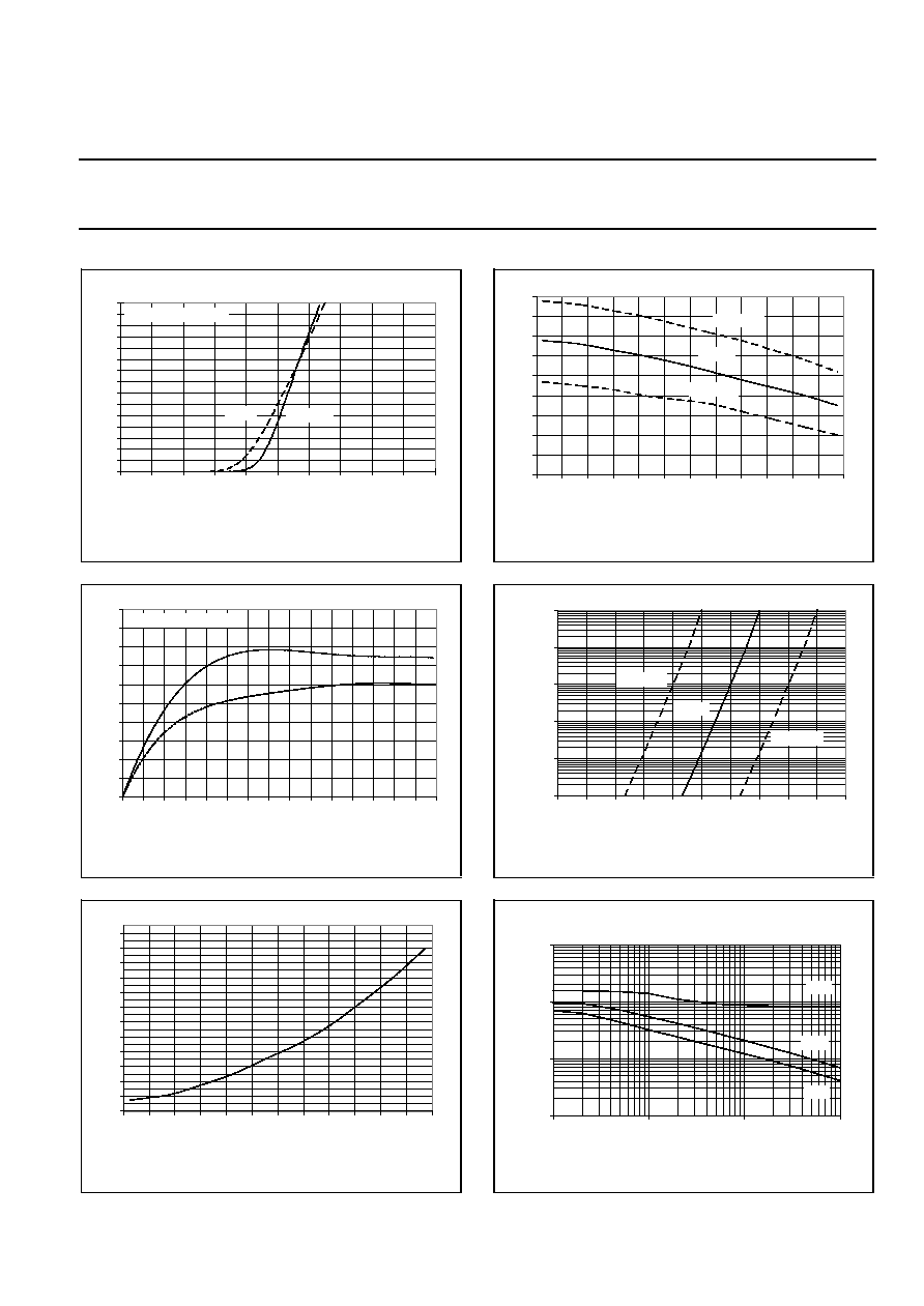
Fig.1. Normalised power dissipation.
PD% = 100
P
D
/P
D 25 ∞C
= f(T
mb
)
Fig.2. Normalised continuous drain current.
ID% = 100
I
D
/I
D 25 ∞C
= f(T
mb
); conditions: V
GS
10 V
Fig.3. Safe operating area. T
mb
= 25 ∞C
I
D
& I
DM
= f(V
DS
); I
DM
single pulse; parameter t
p
Fig.4. Transient thermal impedance.
Z
th j-mb
= f(t); parameter D = t
p
/T
Fig.5. Typical output characteristics, T
j
= 25 ∞C.
I
D
= f(V
DS
)
Fig.6. Typical on-state resistance, T
j
= 25 ∞C.
R
DS(ON)
= f(I
D
)
Normalised Power Derating, PD (%)
0
10
20
30
40
50
60
70
80
90
100
0
25
50
75
100
125
150
175
Mounting Base temperature, Tmb (C)
0.01
0.1
1
10
1E-06
1E-05
1E-04
1E-03
1E-02
1E-01
1E+00
Pulse width, tp (s)
Transient thermal impedance, Zth j-mb (K/W)
single pulse
D = 0.5
0.2
0.1
0.05
0.02
tp
D = tp/T
D
P
T
Normalised Current Derating, ID (%)
0
10
20
30
40
50
60
70
80
90
100
0
25
50
75
100
125
150
175
Mounting Base temperature, Tmb (C)
0
5
10
15
20
25
30
35
40
45
50
55
0
1
2
3
4
5
6
7
8
9
10
Drain-Source Voltage, VDS (V)
Drain Current, ID (A)
4V
5 V
6 V
7 V
9 V
8 V
0.1
1
10
100
1000
1
10
100
1000
Drain-Source Voltage, VDS (V)
Peak Pulsed Drain Current, IDM (A)
D.C.
100 ms
10 ms
RDS(on) = VDS/ ID
1 ms
tp = 10 us
100 us
0
0.1
0.2
0.3
0.4
0.5
0.6
0.7
0.8
0
10
20
30
40
50
Drain Current, ID (A)
Drain-Source On Resistance, RDS(on) (Ohms)
VGS =9 V
8V
6V
7 V
5 V
4V
5.5V
6.5V
August 1999
4
Rev 1.100
Philips Semiconductors
Product specification
N-channel TrenchMOS
TM
transistor
IRF540, IRF540S
Fig.7. Typical transfer characteristics.
I
D
= f(V
GS
)
Fig.8. Typical transconductance, T
j
= 25 ∞C.
g
fs
= f(I
D
)
Fig.9. Normalised drain-source on-state resistance.
R
DS(ON)
/R
DS(ON)25 ∞C
= f(T
j
)
Fig.10. Gate threshold voltage.
V
GS(TO)
= f(T
j
); conditions: I
D
= 1 mA; V
DS
= V
GS
Fig.11. Sub-threshold drain current.
I
D
= f(V
GS)
; conditions: T
j
= 25 ∞C; V
DS
= V
GS
Fig.12. Typical capacitances, C
iss
, C
oss
, C
rss
.
C = f(V
DS
); conditions: V
GS
= 0 V; f = 1 MHz
0
2
4
6
8
10
12
14
16
18
20
22
24
26
28
30
0
1
2
3
4
5
6
7
8
9
10
Gate-source voltage, VGS (V)
Drain current, ID (A)
VDS > ID X RDS(ON)
Tj = 25 C
175 C
Threshold Voltage, VGS(TO) (V)
0
0.5
1
1.5
2
2.5
3
3.5
4
4.5
-60
-40
-20
0
20
40
60
80
100 120 140 160 180
Junction Temperature, Tj (C)
typical
maximum
minimum
0
2
4
6
8
10
12
14
16
18
20
0
2
4
6
8
10 12 14 16 18 20 22 24 26 28 30
Drain current, ID (A)
Transconductance, gfs (S)
Tj = 25 C
175 C
VDS > ID X RDS(ON)
Drain current, ID (A)
1.0E-06
1.0E-05
1.0E-04
1.0E-03
1.0E-02
1.0E-01
0
0.5
1
1.5
2
2.5
3
3.5
4
4.5
5
Gate-source voltage, VGS (V)
minimum
typical
maximum
Normalised On-state Resistance
0.5
0.7
0.9
1.1
1.3
1.5
1.7
1.9
2.1
2.3
2.5
2.7
2.9
-60
-40
-20
0
20
40
60
80
100 120 140 160 180
Junction temperature, Tj (C)
10
100
1000
10000
0.1
1
10
100
Drain-Source Voltage, VDS (V)
Capacitances, Ciss, Coss, Crss (pF)
Ciss
Coss
Crss
August 1999
5
Rev 1.100