Philips Semiconductors
Product specification
74ALVCH16646
16-bit bus transceiver/register (3-State)
2
1998 Sep 03
853-2116 19959
FEATURES
∑
Complies with JEDEC standard no. 8-1A
∑
CMOS low power consumption
∑
MULTIBYTE
TM
flow-through pin-out architecture
∑
Low inductance, multiple V
CC
and ground pins for minimum noise
and ground bounce
∑
Direct interface with TTL levels
∑
Current drive
±
24 mA at 3.0 V
∑
Output drive capability 50
transmission lines @ 85
∞
C
∑
All inputs have bushold circuitry
DESCRIPTION
The 74ALVCH16646 consists of 16 non-inverting bus transceiver
circuits with 3-State outputs, D-type flip-flops and control circuitry
arranged for multiplexed transmission of data directly from the
internal registers. Data on the `A' or `B' bus will be clocked in the
internal registers, as the appropriate clock (CP
AB
or CP
BA
) goes to a
HIGH logic level. Output enable (OE) and direction (DIR) inputs are
provided to control the transceiver function. In the transceiver mode,
data present at the high-impedance port may be stored in either the
`A' or `B' register, or in both. The select source inputs (S
AB
and S
BA
)
can multiplex stored and real-time (transparent mode) data. The
direction (DIR) input determines which bus will receive data when
OE is active (LOW). In the isolation mode (OE = HIGH), `A' data
may be stored in the `B' register and/or `B' data may be stored in the
`A' register.
When an output function is disabled, the input function is still
enabled and may be used to store and transmit data. Only one of
the two buses, `A' or `B' may be driven at a time.
To ensure the high impedance state during power up or power
down, OE should be tied to V
CC
through a pullup resistor; the
minimum value of the resistor is determined by the
current-sinking/current-sourcing capability of the driver.
Active bus-hold circuitry is provided to hold unused or floating data
inputs at a valid logic level.
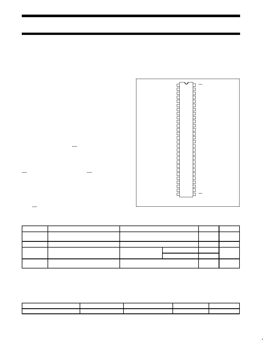
PIN CONFIGURATION
1
2
3
4
5
6
7
8
9
10
11
12
13
14
15
16
17
18
19
20
37
38
39
40
41
42
43
44
45
46
47
48
49
50
51
52
53
54
55
56
1DIR
1CP
AB
1S
AB
GND
1A0
1A1
V
CC
1A3
1A4
GND
1A5
1A6
1A7
2A0
1A2
2A1
2A2
GND
2A3
2A4
2B4
2B3
GND
2B2
2B1
2B0
1B7
1B6
1B5
GND
1B4
1B3
1B2
V
CC
1B1
1B0
GND
1S
BA
1CP
BA
1OE
21
22
23
24
33
34
35
36
2A5
V
CC
2A6
2A7
2B7
2B6
V
CC
2B5
25
26
27
28
29
30
31
32
GND
2S
AB
2CP
AB
2DIR
2OE
2CP
BA
2S
BA
GND
SY00011
QUICK REFERENCE DATA
GND = 0V; T
amb
= 25
∞
C; t
r
= t
f
2.5ns
SYMBOL
PARAMETER
CONDITIONS
TYPICAL
UNIT
t
PHL
/t
PLH
Propagation delay
nAx to nBx
V
CC
= 2.5V, C
L
= 30pF
V
CC
= 3.3V, C
L
= 50pF
2.6
2.7
ns
C
I
Input capacitance
3.0
pF
C
Power dissipation capacitance per channel
V = GND to V
CC
1
Outputs enabled
36
pF
C
PD
Power dissipation capacitance per channel
V
I
= GND to V
CC
1
Outputs disabled
4
pF
F
max
Maximum clock frequency
V
CC
= 2.5V, C
L
= 30pF
V
CC
= 3.3V, C
L
= 50pF
300
320
MHz
NOTES:
1. C
PD
is used to determine the dynamic power dissipation (P
D
in
µ
W):
P
D
= C
PD
◊
V
CC
2
◊
f
i
+
S
(C
L
◊
V
CC
2
◊
f
o
) where:
f
i
= input frequency in MHz; C
L
= output load capacity in pF;
f
o
= output frequency in MHz; V
CC
= supply voltage in V;
S
(C
L
◊
V
CC
2
◊
f
o
) = sum of outputs.
ORDERING INFORMATION
PACKAGES
TEMPERATURE RANGE
OUTSIDE NORTH AMERICA
NORTH AMERICA
DWG NUMBER
56-Pin Plastic TSSOP Type II
≠40
∞
C to +85
∞
C
74ALVCH16646 DGG
ACH16646 DGG
SOT364-1
Philips Semiconductors
Product specification
74ALVCH16646
16-bit bus transceiver/register (3-State)
1998 Sep 03
4
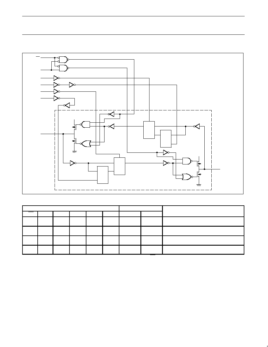
LOGIC DIAGRAM (one section)
S
Y
D
1
MUX
D
2
Q
D
FF
n
CP
S
Y
D
1
MUX
D
2
Q
D
FF
n
CP
V
CC
V
CC
OE
DIR
S
BA
CP
BA
S
AB
CP
AB
An
Bn
8 IDENTICAL CHANNELS
SY00012
FUNCTION TABLE
INPUTS
DATA I/O *
FUNCTION
nOE
nDIR
nCP
AB
nCP
BA
nS
AB
nS
BA
nAx
nBx
FUNCTION
X
X
X
X
X
X
X
X
X
X
input
un*
un*
input
store A, B unspecified*
store B, A unspecified*
H
H
X
X
H or L
H or L
X
X
X
X
input
input
store A and B data, isolation
hold storage
L
L
L
L
X
X
X
H or L
X
X
L
H
output
input
real-time B data to A bus
stored B data to A bus
L
L
H
H
X
H or L
X
X
L
H
X
X
input
output
real-time A data to B bus
stored A data to B bus
*
The data output functions may be enabled or disabled by various signals at the OE and DIR inputs. Data input functions are always enabled,
i.e., data at the bus inputs will be stored on every LOW-to-HIGH transition on the clock inputs.
un
= unspecified
H
= HIGH voltage level
L
= LOW voltage level
X
= don't care
= LOW-to-HIGH level transition
Philips Semiconductors
Product specification
74ALVCH16646
16-bit bus transceiver/register (3-State)
1998 Sep 03
5
RECOMMENDED OPERATING CONDITIONS
SYMBOL
PARAMETER
CONDITIONS
LIMITS
UNIT
SYMBOL
PARAMETER
CONDITIONS
MIN
MAX
UNIT
V
CC
DC supply voltage 2.5V range (for max. speed
performance @ 30 pF output load)
2.3
2.7
V
V
CC
DC supply voltage 3.3V range (for max. speed
performance @ 50 pF output load)
3.0
3.6
V
V
I
DC Input voltage range
0
V
CC
V
V
O
DC output voltage range
0
V
CC
V
T
amb
Operating free-air temperature range
≠40
+85
∞
C
t
r
, t
f
Input rise and fall times
V
CC
= 2.3 to 3.0V
V
CC
= 3.0 to 3.6V
0
0
20
10
ns/V
ABSOLUTE MAXIMUM RATINGS
In accordance with the Absolute Maximum Rating System (IEC 134)
Voltages are referenced to GND (ground = 0V)
SYMBOL
PARAMETER
CONDITIONS
RATING
UNIT
V
CC
DC supply voltage
≠0.5 to +4.6
V
I
IK
DC input diode current
V
I
t
0
≠50
mA
V
I
DC input voltage
For control pins
1
≠0.5 to +4.6
V
V
I
DC in ut voltage
For data inputs
1
≠0.5 to V
CC
+0.5
V
I
OK
DC output diode current
V
O
u
V
CC
or V
O
t
0
"
50
mA
V
O
DC output voltage
Note 1
≠0.5 to V
CC
+0.5
V
I
O
DC output source or sink current
V
O
= 0 to V
CC
"
50
mA
I
GND
, I
CC
DC V
CC
or GND current
"
100
mA
T
stg
Storage temperature range
≠65 to +150
∞
C
P
TOT
Power dissipation per package
≠plastic thin-medium-shrink (TSSOP)
For temperature range: ≠40 to +125
∞
C
above +55
∞
C derate linearly with 11.3 mW/K
above +55
∞
C derate linearly with 8 mW/K
850
600
mW
NOTE:
1. The input and output voltage ratings may be exceeded if the input and output current ratings are observed.