 | –≠–ª–µ–∫—Ç—Ä–æ–Ω–Ω—ã–π –∫–æ–º–ø–æ–Ω–µ–Ω—Ç: NE5217 | –°–∫–∞—á–∞—Ç—å:  PDF PDF  ZIP ZIP |
Document Outline
- DESCRIPTION
- APPLICATIONS
- PIN CONFIGURATION
- FEATURES
- ORDERING INFORMATION
- ABSOLUTE MAXIMUM RATINGS
- PIN DESCRIPTIONS
- BLOCK DIAGRAM
- RECOMMENDED OPERATING CONDITIONS
- DC ELECTRICAL CHARACTERISTICS
- AC ELECTRICAL CHARACTERISTICS
- TYPICAL PERFORMANCE CHARACTERISTICS
- THEORY OF OPERATION AND APPLICATION
- PACKAGING
- Data sheet status
- Definitions
- Disclaimers

Philips
Semiconductors
SA5217
Postamplifier with link status indicator
Product specification
Replaces datasheet NE/SA5217 of 1995 Apr 26
IC19 Data Handbook
1998 Oct 07
INTEGRATED CIRCUITS

Philips Semiconductors
Product specification
SA5217
Postamplifier with link status indicator
2
1998 Oct 07
853-1658 20141
DESCRIPTION
The SA5217 is a 75MHz postamplifier system designed to accept
low level high-speed signals. These signals are converted into a
TTL level at the output. The SA5217 can be DC coupled with the
previous transimpedance stage using SA5210, SA5211 or SA5212A
transimpedance amplifiers. The main difference between the
SA5217 and the SA5214 is that the SA5217 does not make the
output of A1 and input of A2 accessible; instead, it brings out the
output of A2 and the input of A8 thus activating the on-chip Schmitt
trigger function by connecting two external capacitors. The result is
that a much longer string of 1s and 0s, in the bit stream, can be
tolerated. This "system on a chip" features an auto-zeroed first
stage with noise shaping, a symmetrical limiting second stage, and a
matched rise/fall time TTL output buffer. The system is
user-configurable to provide adjustable input threshold and
hysteresis. The threshold capability allows the user to maximize
signal-to-noise ratio, thereby insuring a low Bit Error Rate (BER).
An auto-zero loop can be used to replace two input coupling
capacitors with a single Auto Zero (AZ) capacitor. A signal absent
flag indicates when signals are below threshold. The low signal
condition forces the TTL output to the last logic state. User
interaction with this "jamming" system is available. The SA5217 is
packaged in a standard 20-pin surface-mount package and typically
consumes 40mA from a standard 5V supply. The SA5217 is
designed as a companion to the SA5211/5212A and SA5210
transimpedance amplifiers. These differential preamplifiers may be
directly coupled to the postamplifier inputs. The SA5210/5217,
SA5211/5217 or SA5212A/5217 combinations convert nanoamps of
photodetector current into standard digital TTL levels.
APPLICATIONS
∑
Fiber optics
∑
Communication links in Industrial and/or Telecom environment
with high EMI/RFI
∑
Local Area Networks (LAN)
∑
Synchronous Optical Networks (SONET) STS-1
∑
RF limiter
∑
Good for 223
-1 pseudo random bit stream
PIN CONFIGURATION
D
1
Package
LED
CPKDET
THRESH
GNDA
FLAG
JAM
VCCD
VCCA
GNDD
VOUT
IN1B
IN1A
CAZP
CAZN
OUT2B
IN8B
OUT2A
IN8A
RHYST
RPKDET
NOTE:
1. SOL - Released in large SO package only.
1
2
3
4
5
6
7
8
9
10
20
19
18
17
16
15
14
13
12
11
SD00354
Figure 1. Pin Configuration
FEATURES
∑
Postamp for the SA5211/5212A. SA5210 preamplifier family
∑
Wideband operation: typical 75MHz (150MBaud NRZ)
∑
Interstage filtering/equalization possible
∑
Single 5V supply
∑
Low signal flag
∑
Output disable
∑
Link status threshold and hysteresis programmable
∑
LED driver (normally ON with above threshold signal)
∑
Fully differential for excellent PSRR
∑
Auto-zero loop for DC offset cancellation
∑
2kV ElectroStatic Discharge (ESD) protection
ORDERING INFORMATION
DESCRIPTION
TEMPERATURE RANGE
ORDER CODE
DWG #
20-Pin Plastic Small Outline Large (SOL) Package
-40 to +85
∞
C
SA5217D
SOT163-1
ABSOLUTE MAXIMUM RATINGS
SYMBOL
PARAMETER
SA5214
UNIT
V
CCA
Power supply
+6
V
V
CCD
Power supply
+6
V
T
A
Operating ambient temperature range
-40 to +85
∞
C
T
J
Operating junction temperature range
-55 to +150
∞
C
T
STG
Storage temperature range
-65 to +150
∞
C
P
D
Power dissipation
1.4
W
V
IJ
Jam input voltage
-0.5 to 5.5
V
Philips Semiconductors
Product specification
SA5217
Postamplifier with link status indicator
1998 Oct 07
3
PIN DESCRIPTIONS
PIN
NO.
SYMBOL
DESCRIPTION
1
LED
Output for the LED driver. Open collector output transistor with 125
series limiting resistor. An above threshold signal
turns this transistor ON.
2
C
PKDET
Capacitor for the peak detector. The value of this capacitor determines the detector response time to the signal, supple-
menting the internal 10pF capacitor.
3
THRESH
Peak detector threshold resistor. The value of this resistor determines the threshold level of the peak detector.
4
GND
A
Device analog ground pin.
5
FLAG
Peak detector digital output. When this output is LOW, there is data present above the threshold. This pin is normally
connected to the JAM pin and has a TTL fanout of two.
6
JAM
Input to inhibit data flow. Sending the pin HIGH forces TTL DATA OUT ON, Pin 10, LOW. This pin is normally connected
to the FLAG pin and is TTL-compatible.
7
V
CCD
Power supply pin for the digital portion of the chip.
8
V
CCA
Power supply pin for the analog portion of the chip.
9
GND
D
Device digital ground pin.
10
V
OUT
TTL output pin with a fanout of five.
11
R
PKDET
Peak detector current resistor. The value of this resistor determines the amount of discharge current available to the
peak detector capacitor, C
PKDET
.
12
R
HYST
Peak detector hysteresis resistor. The value of this resistor determines the amount of hysteresis in the peak detector.
13
IN
8A
Non-inverting input to amplifier A8.
14
OUT
2A
Non-inverting output of amplifier A2.
15
IN
8B
Inverting input to amplifier A8.
16
OUT
2B
Inverting output of amplifier A2.
17
C
AZN
Auto-Zero capacitor pin (Negative terminal). The value of this capacitor determines the low-end frequency response of
the preamp A1.
18
C
AZP
Auto-Zero capacitor pin (Positive terminal). The value of this capacitor determines the low-end frequency response of the
preamp A1.
19
IN
1A
Non-inverting input of the preamp A1.
20
IN
1B
Inverting input of the preamp A1.
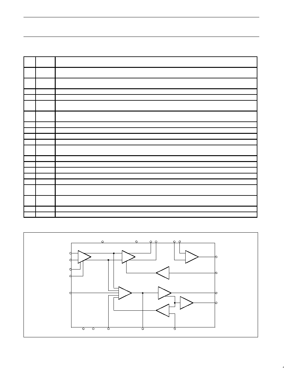
BLOCK DIAGRAM
20
19
18
17
16
15
14
13
12
11
10
9
8
7
6
5
4
3
2
1
A1
A2
A3
A4
A5
A6
A7
GATED AMP
SCHMITT TRIGGER
OUTPUT DISABLE
PEAK DETECT
LED DRIVER
HYSTERESIS
VCCA
VCCD OUT2A OUT2B
A8
IN8B IN8A
VOUT
JAM
FLAG
LED
IN1B
IN1A
CAZP
CAZN
RPKDET
GNDA
GNDD
THRESH
CPKDET
RHYST
SD00355
Figure 2. Block Diagram
Philips Semiconductors
Product specification
SA5217
Postamplifier with link status indicator
1998 Oct 07
4
RECOMMENDED OPERATING CONDITIONS
SYMBOL
PARAMETER
RATING
UNIT
V
CCA
Power supply
4.5 to 5.5
V
V
CCD
Power supply
4.5 to 5.5
V
T
A
Ambient temperature range
-40 to +85
∞
C
T
J
Operating junction temperature range
-40 to +110
∞
C
P
D
Power dissipation
300
mW
DC ELECTRICAL CHARACTERISTICS
Min and Max limits apply over the operating temperature range at V
CCA
= V
CCD
= +5.0V unless otherwise specified. Typical data applies at
V
CCA
= V
CCD
= +5.0V and T
A
= 25
∞
C.
SYMBOL
PARAMETER
TEST CONDITIONS
LIMITS
UNIT
SYMBOL
PARAMETER
TEST CONDITIONS
Min
Typ
Max
UNIT
I
CCA
Analog supply current
30
41.2
mA
I
CCD
Digital supply current (TTL, Flag, LED)
10
13.5
mA
V
I1
A1 input bias voltage (A,B inputs)
3.08
3.4
3.70
V
V
O2
A1 output bias voltage (A,B outputs)
3.10
3.8
4.50
V
V
I8L
A8 input bias voltage Low (A,B inputs)
3.40
3.55
3.68
V
V
I8H
A8 input bias voltage High (A,B inputs)
3.68
3.91
4.12
V
V
OH
High-level TTL output voltage
I
OH
=-200
µ
A
2.4
3.4
V
V
OL
Low-level TTL output voltage
I
OL
=8mA
0.3
0.4
V
I
OH
High-level TTL output current
V
OUT
=2.4V
-40
-24.4
mA
I
OL
Low-level TTL output current
V
OUT
=0.4V
7.0
30
mA
I
OS
Short-circuit TTL output current
V
OUT
=0.0V
-95
mA
V
THRESH
Threshold bias voltage
Pin 3 Open
0.75
V
V
RPKDET
RPKDET
Pin 11 Open
0.72
V
V
RHYST
RHYST bias voltage
Pin 12 Open
0.72
V
V
IHJ
High-level jam input voltage
2.0
V
V
ILJ
Low-level jam input voltage
0.8
V
I
IHJ
High-level jam input current
V
IJ
=2.7V
30
µ
A
I
ILJ
Low-level jam input current
V
IJ
=0.4V
-485
-240
µ
A
V
OHF
High-level flag output voltage
I
OH
=-80
µ
A
2.4
3.8
V
V
OLF
Low-level flag output voltage
I
OL
=3.2mA
0.33
0.4
V
I
OHF
High-level flag output current
V
OUT
=2.4V
-18
-5
mA
I
OLF
Low-level flag output current
V
OUT
=0.4V
3.25
10
mA
I
SCF
Short-circuit flag output current
V
OUT
=0.0V
-61
-40
-26
mA
I
LEDH
LED ON maximum sink current
V
LED
=3.0V
8
22
80
mA

Philips Semiconductors
Product specification
SA5217
Postamplifier with link status indicator
1998 Oct 07
5
AC ELECTRICAL CHARACTERISTICS
Min and Max limits apply over the operating temperature range at V
CCA
= V
CCD
= +5.0V unless otherwise specified. Typical data applies at
V
CCA
= V
CCD
= +5.0V and T
A
= 25
∞
C.
SYMBOL
PARAMETER
TEST CONDITIONS
LIMITS
UNIT
SYMBOL
PARAMETER
TEST CONDITIONS
Min
Typ
Max
UNIT
f
OP
Maximum operating frequency
Test circuit
60
75
MHz
V
INH
Maximum Functional A1 input signal (single en-
ded)
Test Circuit
1.6
V
P-P
Minimum Functional A1 input signal (single-en-
ded)
Test CIrcuit
6
mV
P-P
Minimum Functional A1 input signal (differential)
3
P P
V
INL
Minimum input sensitivity for output BER
10
≠9
(single-ended)
PRBS = 2
23
1
9
mV
Minimum input sensitivity for output BER
10
≠9
(differential)
PRBS = 2
23
≠1
4.5
mV
P-P
R
IN1
Input resistance (differential at IN
1
)
PRBS = 2
23
≠1
1200
C
IN1
Input capacitance (differential at IN
1
)
2
pF
R
IN8
Input resistance (differential at IN
2
)
2000
C
IN2
Input capacitance (differential at IN
2
)
2
pF
R
OUT2
Output resistance (differential at OUT
2
)
25
C
OUT2
Output capacitance (differential at OUT
2
)
2
pF
V
S
Hysteresis voltage range (single-ended)
Test circuit, T
A
= 25
∞
C
10
mV
V
HYS
Hysteresis voltage range (differential)
A
R
RHYST
=5k R
THRESH
=33k
5
mV
P-P
V
THR
Threshold voltage (single-ended)
(FLAG Low) Test circuit,
@ 50MHz
19
mV
P-P
THR
Threshold voltage (differential)
R
RHYST
=4k R
THRESH
=33k
9.5
P P
t
TLH
TTL Output Rise Time 20% to 80%
Test Circuit
1.3
ns
t
THL
TTL Output Fall Time 80% to 20%
Test Circuit
1.2
ns
t
RFD
t
TLH
/t
THL
mismatch
0.1
ns
t
PWD
Pulse width distortion of output
50mV
P-P
, 1010. . .input
Distortion =
T
H
*
T
L
T
H
)
T
L
10
2
TBD
%
1
2
3
4
5
6
7
8
9
10
20
19
18
17
16
15
14
13
12
11
NE5217
LED
THRESH
FLAG
JAM
125
33k
15pF
400
10k
4k
25
50
VCC
+5V
VIN
VOUT
VOUT
GNDD
VCCA
VCCD
GNDA
CPKDET
IN1B
IN1A
CAZP
CAZN
OUT2B
IN8B
OUT2A
IN8A
RHYST
RPKDET
0.1
µ
F
0.1
µ
F
0.1
µ
F
0.1
µ
F
0.1
µ
F
0.1
µ
F
0.1
µ
F
10
µ
F
100
µ
H
100
µ
H
SD00356
Figure 3. AC Test Circuit

Philips Semiconductors
Product specification
SA5217
Postamplifier with link status indicator
1998 Oct 07
6
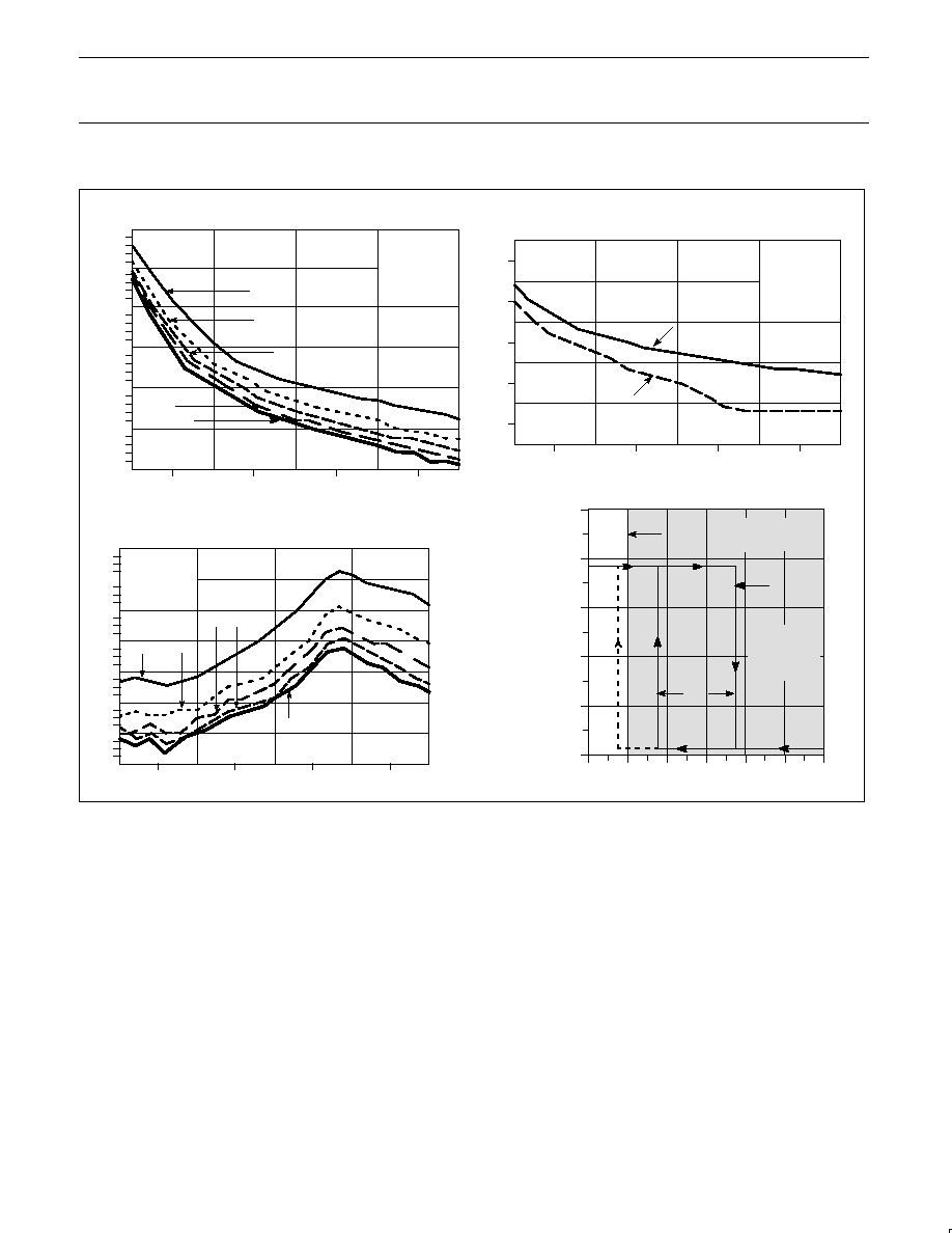
TYPICAL PERFORMANCE CHARACTERISTICS
Analog Supply Current vs Temperature
Digital Supply Current vs Temperature
≠60
≠40
≠20
0
20
40
60
80
100
120
36
34
32
30
28
26
24
ANALOG
SUPPL
Y
CURRENT (mA)
VCC = 5.25V
VCC = 5.00V
VCC = 4.75V
TEMPERATURE (
∞
C)
≠60
≠40
≠20
0
20
40
60
80
100
120
12.0
11.5
11.0
10.5
10.0
9.5
9.0
DIGIT
AL
SUPPL
Y
CURRENT (mA)
VCC = 5.25V
VCC = 5.00V
VCC = 4.75V
TEMPERATURE (
∞
C)
SD00357
Figure 4. Typical Performance Characteristics
Philips Semiconductors
Product specification
SA5217
Postamplifier with link status indicator
1998 Oct 07
7
TYPICAL PERFORMANCE CHARACTERISTICS (continued)
Threshold vs R
THRESH
for Different Values of R
HYST
(Driven Single Ended)
30
40
10
20
30
40
50
15
20
25
35
45
6k
5k
4k
3k
2k
THRESHOLD (mV )
P≠P
RTHRESH (k
)
VCC
= 5V
TA
= 27
∞
C
F = 60MHz
On/Off Voltage vs R
THRESH
(Driven Single Ended)
RTHRESH (k
)
0
10
20
30
40
50
10
20
30
40
50
OFF
ON
VCC
= 5V
T
A
= 27
∞
C
F = 60MHz
RHYST
= 4k
V (mV )
IN
P≠P
Hysteresis vs R
THRESH
for Different Values of R
HYST
(Driven Single Ended)
2
4
6
8
10
12
14
16
10
20
30
40
50
6k
5k
4k
3k
2k
VCC
= 5V
TA = 27
∞
C
F = 60MHz
RTHRESH
(k
)
HYST (mV )
P≠P
5
4
3
2
1
0N
0
5
10
15
20
25
30
VHYS
VIN1
RTHRESH = 33k
RHYST
= 4k
VTHR
FORWARD
ACTIVE
REGION
(shaded)
OFF
VIN
(mVP-P)
Hysteresis and Forward Active Region
FLAG (V)
0
SD00358
Figure 5. Typical Performance Characteristics (cont)
THEORY OF OPERATION AND APPLICATION
The SA5217 postamplifier is a highly integrated chip that provides
up to 60dB of gain at 60MHz, to bring mV level signals up to TTL
levels.
The SA5217 contains eight amplifier blocks (see Block Diagram).
The main signal path is made up of a cascade of limiting stages: A1,
A2 and A8. The A3-A4-A7 path performs a wideband full-wave
rectification of the input signal with adjustable hysteresis and decay
times. It outputs a TTL High on the "FLAG" output (Pin 5) when the
input is below a user adjustable threshold. An on-chip LED driver
turns the external LED to the On state when the input signal is
above the threshold. In a typical application the "FLAG" output is
tied back tot he "JAM" input; forcing the "JAM" input to TTL High will
latch the TTL Data Out at the last logical state.
Threshold voltage and hysteresis voltage range are adjustable with
resistors R
THRESH
and R
HYST
. The typical values given in the data
sheet will result in performance shown in the graph "Hysteresis and
Forward Active Region". A minority of parts may be sensitive
enough that FLAG High (Off) occurs below the minimum functional
input signal level, V
IN1
. This condition is shown by the dotted line in
the graph. Such parts may require adjustment of R
THRESH
if it is
important to guarantee that an output signal is present for the full
hysteresis range. If this is not important, R
THRESH
may be adjusted
to give a FLAG Low for lower level input signals.
An auto-zero loop allows the SA5217 to be directly connected to a
transimpedance amplifier such as the SA5210, SA5211, or
SA5212A without coupling capacitors. This auto-zero loop cancels
the transimpedance amplifier's DC offset, the SA5217 A1 offset, and
the data-dependent offset in the PIN diode/transimpedance amplifier
combination.
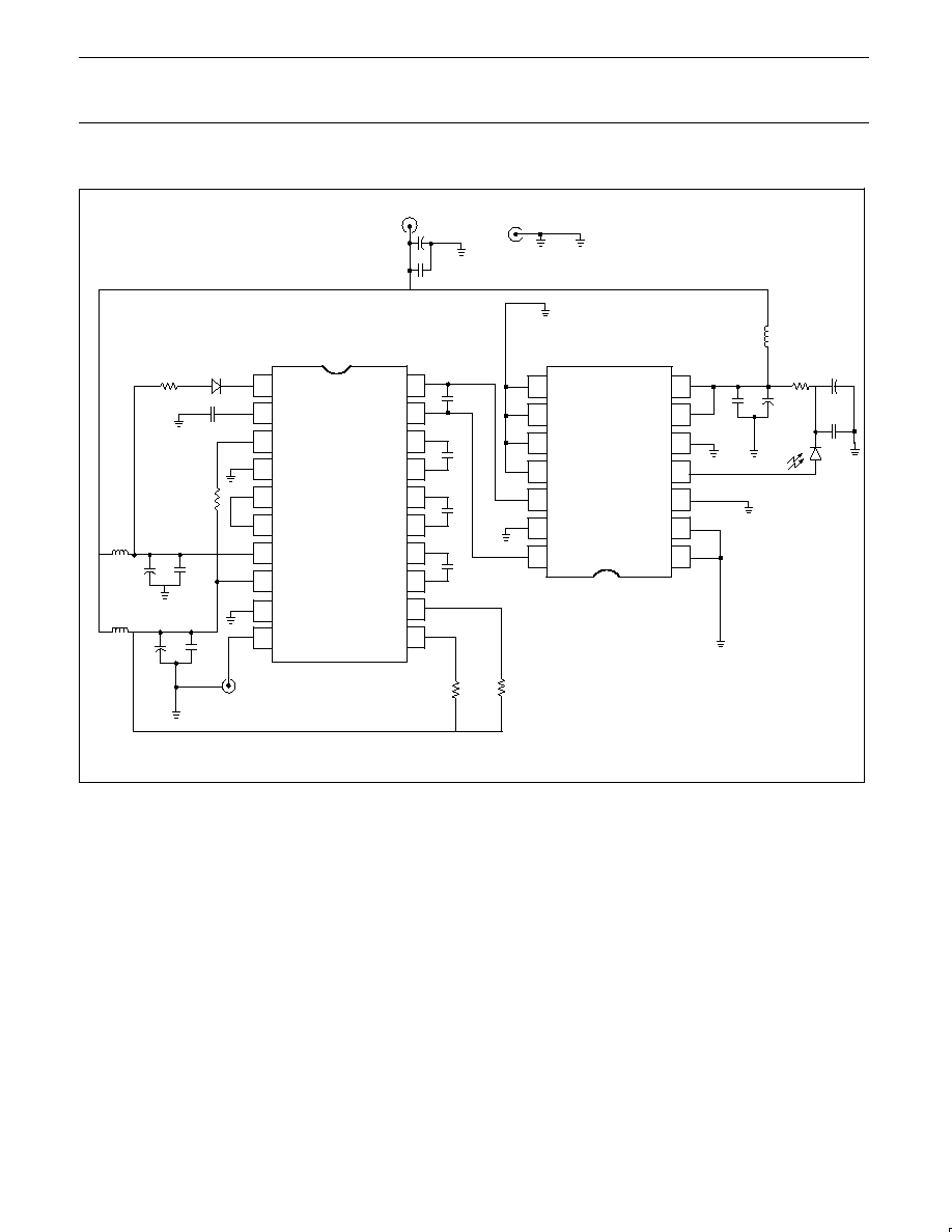
A typical application of the SA5217 postamplifier is depicted in
Figure 6. The system uses the SA5211 transimpedance amplifier
which has a 28k differential transimpedance gain and a -3dB
bandwidth of 140MHz. this typical application is optimized for a
50Mb/s Non Return to Zero (NRZ) bit stream.
As the system's gain bandwidth product is very high, it is crucial to
employ good RF design and printed circuit board layout techniques
to prevent the system from becoming unstable.
Philips Semiconductors
Product specification
SA5217
Postamplifier with link status indicator
1998 Oct 07
8
1
2
3
4
5
6
7
8
9
10
11
12
13
14
15
16
17
18
19
20
1
2
3
4
5
6
7
8
9
10
11
12
13
14
LED
CPKDET
THRESH
GNDA
FLAG
JAM
VCCD
VCCA
GNDD
TTLOUT
IN1B
IN1A
CAZP
CAZN
OUT2B
IN8B
OUT2A
IN8A
RHYST
RPKDET
NE5217
GND
GND
GND
OUT1
GND
GND
OUT2
VCC1
VCC2
NC
IIN
NC
GND
GND
NE5210
R2
220
D1
LED
C11
100pF
100pF
C7
.01
µ
F
47
µ
F
C1
C2
GND
+VCC
0.1
µ
F
0.1
µ
F
0.1
µ
F
R4
4k
R3
33k
VOUT (TTL)
L3
10
µ
H
L2
10
µ
H
C12
C13
.01
µ
F
.01
µ
F
C14
C15
10
µ
F
10
µ
F
C8
C9
C10
L1
10
µ
H
BPF31
OPTICAL
INPUT
R1
100
C5
1.0
µ
F
C6
.01
µ
F
.01
µ
F
C4
10
µ
F
C3
NOTE:
THE NE5210/NE5217 combination can operate at data rates in excess of 100Mb/s NRZ
R5
10k
SD00359
Figure 6. A 50Mb/s Fiber Optic Receiver
For more information on this application, please refer to Application
Brief AB1432.
Die Sales Disclaimer
Due to the limitations in testing high frequency and other parameters
at the die level, and the fact that die electrical characteristics may
shift after packaging, die electrical parameters are not specified and
die are not guaranteed to meet electrical characteristics (including
temperature range) as noted in this data sheet which is intended
only to specify electrical characteristics for a packaged device.
All die are 100% functional with various parametrics tested at the
wafer level, at room temperature only (25
∞
C), and are guaranteed to
be 100% functional as a result of electrical testing to the point of
wafer sawing only. Although the most modern processes are
utilized for wafer sawing and die pick and place into waffle pack
carriers, it is impossible to guarantee 100% functionality through this
process. There is no post waffle pack testing performed on
individual die.
Since Philips Semiconductors has no control of third party
procedures in the handling or packaging of die, Philips
Semiconductors assumes no liability for device functionality or
performance of the die or systems on any die sales.
Although Philips Semiconductors typically realizes a yield of 85%
after assembling die into their respective packages, with care
customers should achieve a similar yield. However, for the reasons
stated above, Philips Semiconductors cannot guarantee this or any
other yield on any die sales.
Philips Semiconductors
Product specification
SA5217
Postamplifier with link status indicator
1998 Oct 07
9
………………
………………
………………
………………
………………
………………
………………
………………
1
2
3
4
5
6
7
8
9
10
11
12
13
14
15
16
17
18
19
20
GNDA
GNDD
VCCA
VCCD
ECN No.: 05379
1992 Jan 27
SD00491
THRESH
CPKDET
LED
FLAG
JAM
IN1B
IN1A
CAZP
CAZN
OUT2B
OUT2A
IN8B
IN8A
RHYST
RPKDET
VOUT
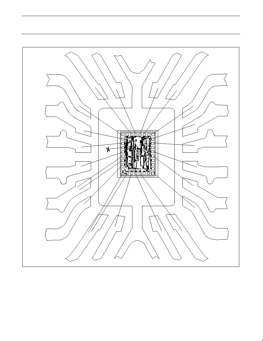
Figure 7. SA5217 Bonding Diagram
Philips Semiconductors
Product specification
SA5217
Postamplifier with link status indicator
1998 Oct 07
10
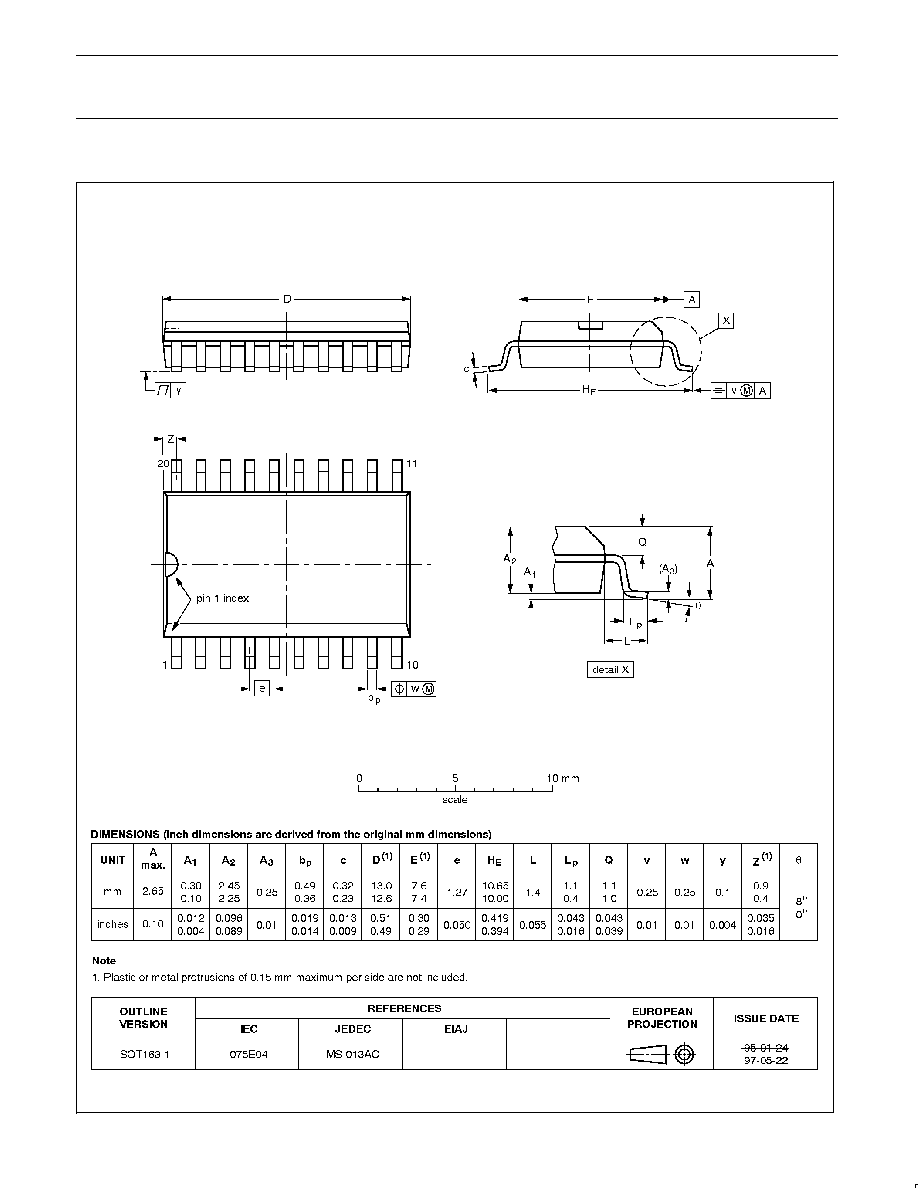
SO20:
plastic small outline package; 20 leads; body width 7.5 mm
SOT163-1

Philips Semiconductors
Product specification
SA5217
Postamplifier with link status indicator
1998 Oct 07
11
NOTES

Philips Semiconductors
Product specification
SA5217
Postamplifier with link status indicator
1998 Oct 07
12
Definitions
Short-form specification -- The data in a short-form specification is extracted from a full data sheet with the same type number and title. For
detailed information see the relevant data sheet or data handbook.
Limiting values definition -- Limiting values given are in accordance with the Absolute Maximum Rating System (IEC 134). Stress above one
or more of the limiting values may cause permanent damage to the device. These are stress ratings only and operation of the device at these or
at any other conditions above those given in the Characteristics sections of the specification is not implied. Exposure to limiting values for extended
periods may affect device reliability.
Application information -- Applications that are described herein for any of these products are for illustrative purposes only. Philips
Semiconductors make no representation or warranty that such applications will be suitable for the specified use without further testing or
modification.
Disclaimers
Life support -- These products are not designed for use in life support appliances, devices or systems where malfunction of these products can
reasonably be expected to result in personal injury. Philips Semiconductors customers using or selling these products for use in such applications
do so at their own risk and agree to fully indemnify Philips Semiconductors for any damages resulting from such application.
Right to make changes -- Philips Semiconductors reserves the right to make changes, without notice, in the products, including circuits, standard
cells, and/or software, described or contained herein in order to improve design and/or performance. Philips Semiconductors assumes no
responsibility or liability for the use of any of these products, conveys no license or title under any patent, copyright, or mask work right to these
products, and makes no representations or warranties that these products are free from patent, copyright, or mask work right infringement, unless
otherwise specified.
Philips Semiconductors
811 East Arques Avenue
P.O. Box 3409
Sunnyvale, California 94088≠3409
Telephone 800-234-7381
©
Copyright Philips Electronics North America Corporation 1998
All rights reserved. Printed in U.S.A.
Date of release: 10-98
Document order number:
9397 750 04627
Philips
Semiconductors
Data sheet
status
Objective
specification
Preliminary
specification
Product
specification
Product
status
Development
Qualification
Production
Definition
[1]
This data sheet contains the design target or goal specifications for product development.
Specification may change in any manner without notice.
This data sheet contains preliminary data, and supplementary data will be published at a later date.
Philips Semiconductors reserves the right to make chages at any time without notice in order to
improve design and supply the best possible product.
This data sheet contains final specifications. Philips Semiconductors reserves the right to make
changes at any time without notice in order to improve design and supply the best possible product.
Data sheet status
[1]
Please consult the most recently issued datasheet before initiating or completing a design.