 | –≠–ª–µ–∫—Ç—Ä–æ–Ω–Ω—ã–π –∫–æ–º–ø–æ–Ω–µ–Ω—Ç: NE5560 | –°–∫–∞—á–∞—Ç—å:  PDF PDF  ZIP ZIP |
Philips Semiconductors
Product specification
NE/SE5560
Switched-mode power supply control circuit
1
1994 Aug 31
853-0125 13721
DESCRIPTION
The NE/SE5560 is a control circuit for use in switched-mode power
supplies. This single monolithic chip incorporates all the control and
housekeeping (protection) functions required in switched-mode
power supplies, including an internal temperature-compensated
reference source, internal Zener references, sawtooth generator,
pulse-width modulator, output stage and various protection circuits.
FEATURES
∑
Stabilized power supply
∑
Temperature-compensated reference source
∑
Sawtooth generator
∑
Pulse-width modulator
∑
Remote on/off switching
∑
Current limiting
∑
Low supply voltage protection
∑
Loop fault protection
∑
Demagnetization/overvoltage protection
∑
Maximum duty cycle clamp
∑
Feed-forward control
∑
External synchronization
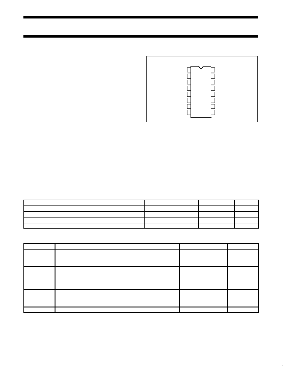
PIN CONFIGURATION
D, F, N Packages
1
2
3
4
5
6
7
8
9
10
11
12
13
14
16
15
VCC
VZ
FEEDBACK
GAIN
MODULATOR
DUTY CYCLE CONTROL
RT
CT
FEEDFORWARD
OUTPUT (COLL)
OUTPUT (EMIT)
DEMAG: OVERVOLTAGE
GND
CURRENT LIMITING
REMOTE ON/OFF
EXTERNAL SYNC
SL00360
Figure 1. Pin Configuration
ORDERING INFORMATION
DESCRIPTION
TEMPERATURE RANGE
ORDER CODE
DWG #
16-Pin Plastic Dual In-Line Package (DIP)
0 to 70
∞
C
NE5560N
SOT38-4
16-Pin Plastic Small Outline Large (SOL) Package
0
∞
C to 70
∞
C
NE5560D
SOT162-1
16-Pin Plastic Dual In-Line Package (DIP)
-55
∞
C to 125
∞
C
SE5560N
SOT38-4
16-Pin Cerdip Dual In-Line Package (CERDIP)
-55
∞
C to 125
∞
C
SE5560F
0582B
ABSOLUTE MAXIMUM RATINGS
SYMBOL
PARAMETER
RATING
UNIT
Supply
1
V
CC
Voltage-forced mode
+18
V
I
CC
Current-fed mode
30
mA
Output transistor (at 20-30V max)
I
OUT
Output current
40
mA
Collector voltage (Pin 15)
V
CC
+1.4V
V
Max. emitter voltage (Pin 14)
+5
V
T
A
Operating ambient temperature range
SE5560
-55 to +125
∞
C
NE5560
0 to 70
∞
C
T
STG
Storage temperature range
-65 to +150
∞
C
NOTES:
1. Does not include current for timing resistors or capacitors.
Philips Semiconductors
Product specification
NE/SE5560
Switched-mode power supply control circuit
1994 Aug 31
2
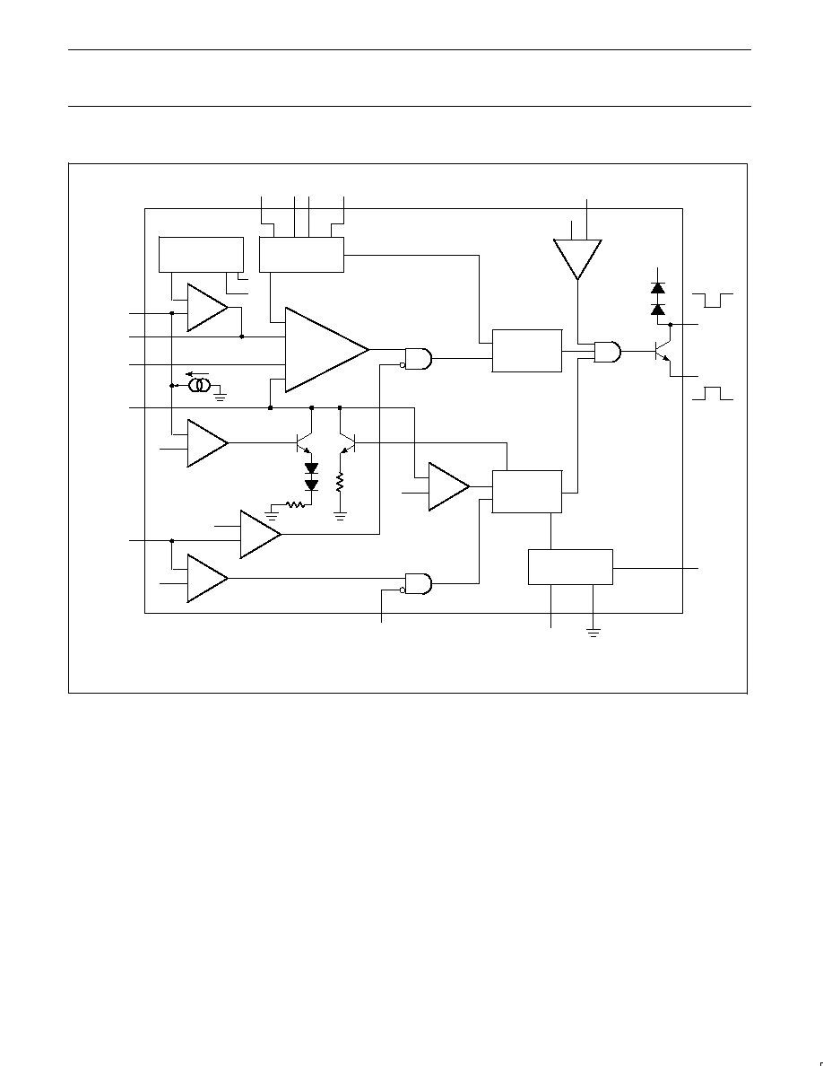
BLOCK DIAGRAM
NOTE:
1. See Voltage/Current fed supply characteristic curve.
FEED
FORWARD
EXTERNAL
SYNC INPUT
DEMAGNETIZATION
OVER-VOLTAGE PROTECTION
REFERENCE
VOLTAGE
SAWTOOTH
GENERATOR
FEEDBACK
VOLTAGE
GAIN ADJUST
MODULATOR
INPUT
CUTY CYCLE
CONTROL
CURRENT
LIMITING
+
≠
0.48V
0.6V
+
0.6V
0.6V
0.48V
+
≠
≠
+
+
≠
≠
+
PULSE WIDTH
MODULATOR
≠
+
0.6V
S
R
LATCH
Q
R
S
START
STOP
REMOTE
ON/OFF
STABILIZED
SUPPLY
+
≠
0.6V
3
4
5
8
11
10
1
12
2
14
15
13
9
8
7
16
OUTPUTS
CT
RT
VZ
VCC
1k
100
OC1
Q1
+
≠
VCC
SL00361
Figure 2. Block Diagram

Philips Semiconductors
Product specification
NE/SE5560
Switched-mode power supply control circuit
1994 Aug 31
3
DC ELECTRICAL CHARACTERISTICS
T
A
=25
∞
C, V
CC
=12V, unless otherwise specified.
SYMBOL
PARAMETER
TEST CONDITIONS
SE5560
NE5560
UNIT
SYMBOL
PARAMETER
TEST CONDITIONS
Min
Typ
Max
Min
Typ
Max
UNIT
Reference sections
V
REF
Internal reference voltage
25
∞
C
3.69
3.72
3.81
3.57
3.72
3.95
V
Over temperature
3.65
3.85
3.53
4.00
V
Temperature coefficient of V
REF
-100
-100
ppm/
∞
C
V
Z
Internal Zener reference
I
L
=-7mA
7.8
8.4
8.8
7.8
8.4
8.8
V
Temperature coefficient of V
Z
200
200
ppm/
∞
C
Oscillator section
Frequency range
Over temperature
50
100k
50
100k
Hz
Initial accuracy oscillator
R=5k
5
5
%
Duty cycle range
f
O
=20kHz
0
98
0
98
%
Modulator
Modulation input current
Voltage at Pin 5=2V Over
temperature
0.2
20
0.2
20
µ
A
Housekeeping function
I
IN`
Pin 6, input current
At 2V
I
IN`
Pin 6, input current
Over temperature
0.2
20
0.2
20
µ
A
Pin 6, duty cycle limit control
Pin 6, duty cycle limit control
For 50% max duty cycle
Pin 6, duty cycle limit control
15kHz to 50kHz/41% of V
Z
40
50
60
40
50
60
% of duty
cycle
Pin 1, low supply voltage
protection thresholds
8
9.0
10.5
8
9.0
10.5
V
Pin 3, feedback loop protection trip
threshold
400
600
720
400
600
720
mV
At 2V
Pin 3, pull-up current
-7
-15
-35
-7
-15
-35
µ
A
Pin 13,
demagnetization/over-voltage
protection trip on threshold
Over temperature
470
600
720
470
600
720
mV
At 0.25V
I
IN
Pin 13, input current
25
∞
C
-0.6
-10
-0.6
-10
µ
A
Over temperature
-20
-20
Pin 16, feed-forward duty cycle
control
Voltage at Pin 16=2V
Z
30
40
50
30
40
50
% original
duty cycle
At 16V, V
CC
=18V
*Pin 16, feed-forward input current
25
∞
C
0.2
5
0.2
5
µ
A
Over temperature
10
10
µ
A
External synchronization
Pin 9 Off
0
0.8
0
0.8
V
On
2
V
Z
2
V
Z
V
Sink current
Voltage at Pin 9=0V, 25
∞
C
-65
-100
-65
-125
µ
A
Over temperature
-125
-125
µ
A
Remote
Pin 10 Off
0
0.8
0
0.8
V
On
2
V
Z
2
V
Z
V
At 0V
Sink current
25
∞
C
-85
-100
-85
-125
µ
A
Over temperature
-125
-125
µ
A

Philips Semiconductors
Product specification
NE/SE5560
Switched-mode power supply control circuit
1994 Aug 31
4
DC ELECTRICAL CHARACTERISTICS
(Continued)
SYMBOL
PARAMETER
TEST CONDITIONS
SE5560
NE5560
UNIT
SYMBOL
PARAMETER
TEST CONDITIONS
Min
Typ
Max
Min
Typ
Max
UNIT
Current limiting
I
IN
Pin 11 Input current
Voltage at
Pin 11=250mV
-2
-20
-2
-20
µ
A
25
∞
C
Over temperature
-40
-40
µ
A
Single pulse inhibit delay
Inhibit delay time for 20%
overdrive at 40mA I
OUT
0.7
0.8
0.7
0.8
µ
s
OC2
Trip Levels: Shut down, slow start,
low level
0.500
0.600
0.700
0.500
0.600
0.700
V
OC1
Current limit, high level
0.400
0.480
0.560
0.400
0.560
0.500
V
OC
Low Level in terms of high level,
OC
2
0.750
0.800
0.850
0.750
0.800
0.850
V
Error amplifier
V
OH
Output voltage swing
6.2
9.5
6.2
9.5
V
V
OL
Output voltage swing
0.7
0.7
V
Open-loop gain
54
60
54
60
dB
R
F
Feedback resistor
10k
10k
BW
Small-signal bandwidth
3
3
MHz
Output stage
V
CE
(SAT) I
C
=40mA
0.5
0.5
V
Output current (Pin 15)
40
40
mA
Max. emitter voltage (Pin 14)
5
6
5
6
V
Supply voltage/current
1
I
CC
Supply current
I
Z
=0, voltage-forced,
V
CC
=12V, 25
∞
C
10
10
mA
Over temp.
15
15
mA
V
CC
Supply voltage
I
CC
=10mA current-fed
20
23
19
24
V
V
CC
Supply voltage
I
CC
=30mA current-fed
20
30
20
30
V
NOTES:
1. Does not include current for timing resistors or capacitors.

Philips Semiconductors
Product specification
NE/SE5560
Switched-mode power supply control circuit
1994 Aug 31
5
MAXIMUM PIN VOLTAGES
NE5560
Pin No
Function
Maximum Voltage
1
V
CC
See Note 1
2
V
Z
Do not force (8.4V)
3
Feedback
V
Z
4
Gain
5
Modulator
V
Z
6
Duty Cycle Control
V
Z
7
R
T
Current force mode
8
C
T
9
External Sync
V
Z
10
Remote On/Off
V
Z
11
Current Limiting
V
CC
12
GND
GND
13
Demagnetization/Overvoltage
V
CC
14
Output (Emit)
V
Z
15
Output (Collector)
V
CC
+2V
BE
16
Feed-forward
V
CC
NOTES:
1. When voltage-forced, maximum is 18V; when current-fed, maximum is 30mA. See voltage-/current-fed supply characteristic curve.
TYPICAL PERFORMANCE CHARACTERISTICS
60
50
40
30
20
10
0
1k
10k
100k
1M
10M
FREQUENCY (Hz)
GAIN (dB)
Open-Loop Gain
0
≠30
≠60
≠90
≠120
≠150
≠180
1k
10k
100k
1M
10M
FREQUENCY (Hz)
PHASE
ANGLE (DEG)
Open-Loop Phase
Error Amplifier
SL00362
Figure 3. Typical Performance Characteristics

Philips Semiconductors
Product specification
NE/SE5560
Switched-mode power supply control circuit
1994 Aug 31
6
TYPICAL PERFORMANCE CHARACTERISTICS
(Continued)
MAX (%)
(%)
V
CC
Pd MAX (W)
1.0
50
24
TA
OPERATING CURVE
≠60
∞
C
25
∞
C
70
∞
C
125
∞
C
SE
NE
Power Derating Curve
mA
20
10
0
0
10
20
30
V
NE5560
Voltage-/Current-Fed
Supply Characteristics
VCC
GND
12
1
VS
RVCC
VCC
Current-Fed Dropping Resistor
SEE DC ELECTRICAL
CHARACTERISTICS
FOR CURRENT FED
VCC RANGE
R
VCC
+
V
S
*
V
CC
(10 20mA)
100
90
80
70
60
50
40
30
20
10
0
1
2
3
4
5
6
V4,5,6 (V)
Transfer Curve of Pulse-Width
Modular Duty Cycle vs Input Voltage
12
R1
R2
2
6
DUTY
CYCLE
CONTROL
MAXIMUM DUTY
CYCLE (%)
100
90
80
70
60
50
40
30
20
10
0
0.1 0.2
0.3 0.4 0.5 0.6 0.7 0.8 0.9 1
R
2
R
1
*
R
2
Graph for Determining
MAX
(%)
R1 + R2
(
)
SOFT ST
ART DUTY
CYCLE %
103
104
2
3
4
5
6 7 8 9
2
80
70
60
50
40
30
20
10
MAX 90%
MAX 70%
MAX 50%
MAX 30%
≠
+
7
6
5
4
3
2
1
0.9
0.8
0.7
0.6
0.5
0.4
0.3
0.2
0.1
4
3
RS
R1
VREF(3.72V)
VO/VREF (%)
10
20
30
40
50
60
70
80
90
Regulation vs Error
Amp Closed Gain
Soft-Start Min. Duty Cycle vs R
1
+ R
2
R
f
R
S
+
20
R
f
R
S
+
100
R
f
R
S
+
500
SL00363
Figure 4. Typical Performance Characteristics

Philips Semiconductors
Product specification
NE/SE5560
Switched-mode power supply control circuit
1994 Aug 31
7
TYPICAL PERFORMANCE CHARACTERISTICS
(Continued)
DUTY
CYCLE
1000
100
90
80
70
60
50
40
30
20
10
9
8
7
6
5
4
3
2
1
R=10k
R=20k
R=40k
R=5k
2
2.5
3
3.5
4
4.5
CnF)
f(kHz)
Typical Frequency Plot vs R
T
and
C
T
100
90
80
70
60
50
40
30
20
10
1
1.5
2
2.5
V
16
V
Z
SL00364
Figure 5. Typical Performance Characteristics
THEORY OF OPERATION
The following functions are incorporated:
≠ A temperature-compensated reference source.
≠ An error amplifier with Pin 3 as input. The output is connected
to Pin 4 so that the gain is adjustable with external resistors.
≠ A sawtooth generator with a TTL-compatible synchronization
input (Pins 7, 8, 9).
≠ A pulse-width modulator with a duty cycle range from 0 to 95%.
The PWM has two additional inputs:
Pin 6 can be used for a precise setting of
MAX
Pin 5 gives a direct access to the modulator, allowing for real
constant-current operation:
≠ A gate at the output of the PWM provides a simple dynamic
current limit.
≠ A latch that is set by the flyback of the sawtooth and reset by
the output pulse of the above mentioned gate prohibits double
pulsing.
≠ Another latch functions as a start-stop circuit; it provides a fast
switch-off and a slow start.
≠ A current protection circuit that operates via the start-stop
circuit. This is a combined function with the current limit circuit,
therefore Pin 11 has two trip-on levels; the lower one for
cycle-by-cycle current limiting, the upper one for current
protection by means of switch-off and slow-start.
≠ A TTL-compatible remote on/off input at Pin 10, also operating
via the start-stop circuit.
≠ An inhibit input at Pin 13. The output pulse can be inhibited
immediately.
≠ An output gate that is commanded by the latches and the inhibit
circuit.
≠ An output transistor of which both the collector (Pin 15) and the
emitter (Pin 14) are externally available. This allows for normal
or inverse output pulses.
≠ A power supply that can be either voltage- or current-driven
(Pins 1 and 12). The internally-generated stabilized output
voltage VZ is connected to Pin 2.
≠ A special function is the so-called feed-forward at Pin 16. The
amplitude of the sawtooth generator is modulated in such a way
that the duty cycle becomes inversely proportional to the
voltage on this pin:
~ 1/V16.
≠ Loop fault protection circuits assure that the duty cycle is
reduced to zero or a low value for open- or short-circuited
feedback loops.
Stabilized Power Supply (Pins 1, 2, 12)
The power supply of the NE5560 is of the well known series
regulation type and provides a stabilized output voltage of typically
8.5V.
This voltage V
Z
is also present at Pin 2 and can be used for precise
setting of
MAX
and to supply external circuitry. Its max. current
capability is 5mA.
The circuit can be fed directly from a DC voltage source between
10.5V and 18V or can be current-driven via a limiting resistor. In the
latter case, internal pinch-off resistors will limit the maximum supply
voltage: typical 23V for 10mA and max. 30V for 30mA.
The low supply voltage protection is active when V
(1-12)
is below
10.5V and inhibits the output pulse (no hysteresis).
When the supply voltage surpasses the 10.5V level, the IC starts
delivering output pulses via the slow-start function.

Philips Semiconductors
Product specification
NE/SE5560
Switched-mode power supply control circuit
1994 Aug 31
8
The current consumption at 12V is less than 10mA, provided that no
current is drawn from V
Z
and R
(7-12)
20k
.
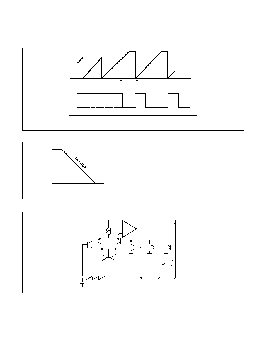
The Sawtooth Generator
Figure 6 shows the principal circuitry of the oscillator. A resistor
between Pin 7 and Pin 12 (GND) determines the constant current
that charges the timing capacitor C
(8-12)
.
This causes a linear increasing voltage on Pin 8 until the upper level
of 5.6V is reached. Comparator H sets the RS flip-flop and Q1
discharges C
(8-12)
down to 1.1V, where comparator L resets the
flip-flop. During this flyback time, Q2 inhibits the output.
Synchronization at a frequency lower than the free-running
frequency is accomplished via the TTL gate on Pin 9. By activating
this gate (V
9
<2V), the setting of the sawtooth is prevented. This is
indicated in Figure 7.
Figure 8 shows a typical plot of the oscillator frequency against the
timing capacitor. The frequency range of the NE5560 goes from
<50Hz up to >100kHz.
Reference Voltage Source
The internal reference voltage source is based on the bandgap
voltage of silicon. Good design practice assures a temperature
dependency typically
±
100ppm/
∞
C. The reference voltage is
connected to the positive input of the error amplifier and has a
typical value of 3.72V.
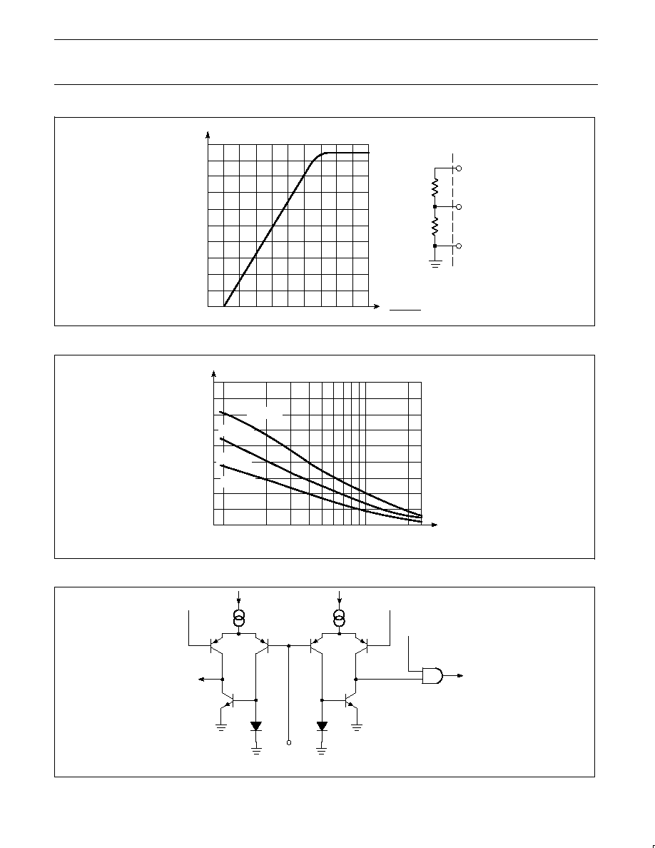
Error Amplifier Compensation
For closed-loop gains less than 40dB, it is necessary to add a
simple compensation capacitor as shown in Figures 8 and 9.
Error Amplifier with Loop-Fault Protection Circuits
This operational amplifier is of a generally used concept and has an
open-loop gain of typically 60dB. As can be seen in Figure 9, the
inverting input is connected to Pin 3 for a feedback information
proportional to V
O
.
The output goes to the PWM circuit, but is also connected to Pin 4,
so that the required gain can be set with R
S
and R
(3-4)
. This is
indicated in Figure 9, showing the relative change of the feedback
voltage as a function of the duty cycle. Additionally, Pin 4 can be
used for phase shift networks that improve the loop stability.
When the SMPS feedback loop is interrupted, the error amplifier
would settle in the middle of its active region because of the
feedback via R
(3-4)
. This would result in a large duty cycle. A current
source on Pin 3 prevents this by pushing the input voltage high via
the voltage drop over R
(3-4)
. As a result, the duty cycle will become
zero, provided that R
(3-4)
>100k. When the feedback loop is
short-circuited, the duty cycle would jump to the adjusted maximum
duty cycle. Therefore, an additional comparator is active for
feedback voltages at Pin 3 below 0.6V. Now an internal resistor of
typically 1k is shunted to the impedance on the
MAX
setting Pin 6.
Depending on this impedance,
will be reduced to a value
0
. This
will be discussed further.
The Pulse-Width Modulator
The function of the PWM circuit is to translate a feedback voltage
into a periodical pulse of which the duty cycle depends on that
feedback voltage. As can be seen in Figure 10, the PWM circuit in
the NE5560 is a long-tailed pair in which the sawtooth on Pin 8 is
compared with the LOWEST voltage on either Pin 4 (error amplifier),
Pin 5, or Pin 6 (
MAX
and slow-start). The transfer graph is given in
Figure 11. The output of the PWM causes the resetting of the output
bi-stable.
Limitation of the Maximum Duty Cycle
With Pins 5 and 6 not connected and with a rather low feedback
voltage on Pin 3, the NE5560 will deliver output pulses with a duty
cycle of
95%. In many SMPS applications, however, this high
will
cause problems. Especially in forward converters, where the
transformer will saturate when
exceeds 50%, a limitation of the
maximum duty cycle is a must.
A DC voltage applied to Pin 6 (PWM input) will set
MAX
at a value
in accordance with Figure 11. For low tolerances of
MAX
, this
voltage on Pin 6 should be set with a resistor divider from V
Z
(Pin 2).
The upper and lower sawtooth levels are also set by means of an
internal resistor divider from V
Z
, so forming a bridge configuration
with the
MAX
setting is low because tolerances in V
Z
are
compensated and the sawtooth levels are determined by internal
resistor matching rather than by absolute resistor tolerance. Figure
12 can be used for determining the tap on the bleeder for a certain
MAX
setting.
As already mentioned, Figure 13 gives a graphical representation of
this. The value
o is limited to the lower and the higher side;
∑
It must be large enough to ensure that at maximum load and mini-
mum input voltage the resulting feedback voltage on Pin 3
exceeds 0.6V.
∑
It must be small enough to limit the amount of energy in the SMPS
when a loop fault occurs. In practice, a value of 10-15% will be a
good compromise.
SET
RESET
7
8
1.1V
5.6V
N
L
≠
+
≠
+
Q1
Q2
TO OUTPUT LATCH
TO PWM
9 SYN
VZ
RT
CT
SL00365
Figure 6. Sawtooth Generator
Philips Semiconductors
Product specification
NE/SE5560
Switched-mode power supply control circuit
1994 Aug 31
9
5.6V
1.1V
INHIBIT
`SET'
SET
RESET
>2V
<0.8V
VS
VS
SL00366
Figure 7. Sawtooth Oscillator Synchronization
60dB
SLOPE
20dB/DECADE
1kHz
10kHz
1MHz
SL00367
Figure 8. Error Amplifier Compensation Open-Loop Gain
(+)
8
3.72V
3
+
≠
ERROR
AMP
PWM
OUT
(≠)
(≠) O.C.
(≠)
START/
STOP
RESET
4
5
6
SL00368
Figure 9. Error Amplifier

Philips Semiconductors
Product specification
NE/SE5560
Switched-mode power supply control circuit
1994 Aug 31
10
a. Duty Cycle --
-- % Regulation
b. Pulse-Width Modulation
(+)
8
3.72V
3
+
≠
ERROR
AMP
PWM
OUT
(≠)
(≠) O.C.
(≠)
START/
STOP
RESET
4
5
6
≠
+
7
6
5
4
3
2
1
0.9
0.8
0.7
0.6
0.5
0.4
0.3
0.2
0.1
4
3
RS
R1
VREF(3.72V)
VO/VREF (%)
10
20
30
40
50
60
70
80
90
R
f
R
S
+
20
R
f
R
S
+
100
R
f
R
S
+
500
SL00369
Figure 10.
100
90
80
70
60
50
40
30
20
10
0
1
2
3
4
5
6
(%)
V4,5,6 (V)
SL00370
Figure 11. Transfer Curve of Pulse-Width Modulator
Duty Cycle vs Input Voltage
Extra PWM Input (Pin 5)
The PWM has an additional inverting input: Pin 5. It allows for
attacking the duty cycle via the PWM circuit, independently from the
feedback and the
MAX
information. This is necessary when the
SMPS must have a real constant-current behavior, possibly with a
fold-back characteristic. However, the realization of this feature must
be done with additional external components. When not used, Pin 5
should be tied to Pin 6.
Philips Semiconductors
Product specification
NE/SE5560
Switched-mode power supply control circuit
1994 Aug 31
11
MAX (%)
12
R1
R2
2
6
DUTY
CYCLE
CONTROL
MAXIMUM DUTY
CYCLE (%)
100
90
80
70
60
50
40
30
20
10
0
0.1
0.2
0.3
0.4
0.5
0.6
0.7
0.8
0.9
1
R
2
R
1
*
R
2
SL00371
Figure 12. Graph for Determining
MAX
(%)
R1 + R2
(
)
SOFT ST
ART DUTY
CYCLE %
103
104
2
3
4
5
6 7 8 9
2
80
70
60
50
40
30
20
10
MAX 90%
MAX 70%
MAX 50%
MAX 30%
SL00372
Figure 13. Soft-Start Minimum Duty Cycle vs R
1
+ R
2
0.6V
START
STOP
11
0.48V
from
PWM
RESET
OF OUTPUT
BISTABLE
SL00373
Figure 14. Current Protection Input
Philips Semiconductors
Product specification
NE/SE5560
Switched-mode power supply control circuit
1994 Aug 31
12
V11 (CURRENT LIMITING)
NORMAL OPERATING
POINT
LEVEL 1 LEVEL 2
.48
.60 (V)
RELA
TIVE I (mA)
OUT
OC1
OC2
SL00374
Figure 15. Output Characteristics
Dynamic Current Limit and Current Protection
(Pin 11)
In many applications, it is not necessary to have a real
constant-current output of the SMPS.
Protection of the power transistor will be the prime goal. This can be
realized with the NE5560 in an economical way. A resistor (or a
current transformer) in the emitter of the power transistor gives a
replica of the collector current. This signal must be connected to Pin
11. As can be seen in Figure 14, this input has two comparators with
different reference levels. The output of the comparator with the
lower 0.48V reference is connected to the same gate as the output
of the PWM.
When activated, it will immediately reset the output flip-flop, so
reducing the duty cycle. The effectiveness of this cycle-by-cycle
current limit diminishes at low duty cycle values. When
becomes
very small, the storage time of the power transistor becomes
dominant. The current will now increase again, until it surpasses the
reference of the second comparator. The output of this comparator
activates the start-stop circuit and causes an immediate inhibit of the
output pulses. After a certain deadtime, the circuit starts again with
very narrow output pulses. The effect of this two-level current
protection circuit is visualized in Figure 15.
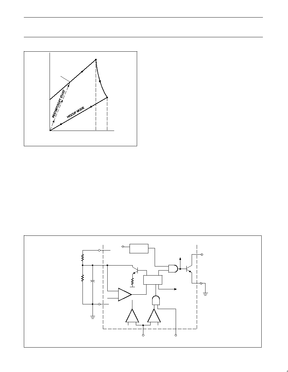
The Start-Stop Circuit
The function of this protection circuit is to stop the output pulses as
soon as a fault occurs and to keep the output stopped for several
periods. After this dead-time, the output starts with a very small,
gradually increasing duty cycle. When the fault is persistent, this will
cause a cyclic switch-off/switch-on condition. This "hiccup" mode
effectively limits the energy during fault conditions. The realization
and the working of the circuit are indicated in Figures 12 and 13.
The dead time and the soft-start are determined by an external
capacitor that is connected to Pin 6 (
MAX
setting).
An RS flip-flop can be set by three different functions:
1. Remote on/off on Pin 10.
2. Overcurrent protection on Pin 11.
3. Low supply voltage protection (internal).
As soon as one of these functions cause a setting of the flip-flop, the
output pulses are blocked via the output gate. In the same time
transistor Q1 is forward-biased, resulting in a discharge of the
capacitor on Pin 6.
The discharging current is limited by an internal 150
resistor in the
emitter of Q1. The voltage at Pin 6 decreases to below the lower
level of the sawtooth. When V6 has dropped to 0.6V, this will
activate a comparator and the flip-flop is reset. The output stage is
no longer blocked and Q1 is cut off. Now V
Z
will charge the
capacitor via R1 to the normal
MAX
voltage. The output starts
delivering very narrow pulses as soon as V6 exceeds the lower
sawtooth level. The duty cycle of the output pulse now gradually
increases to a value determined by the feedback on Pin 3, or by the
static
MAX
setting on Pin 6.
15
14
2
6
12
11
10
LATCH
START/
STOP
SET
RESET
0.6V
0.48V
0.6V
LOW SUPPLY
VOLTAGE
PROTECTION
100
R1
R2
CSS
Q1
Q2
PWM
VZ
SL00375
Figure 16. Start-Stop Circuit

Philips Semiconductors
Product specification
NE/SE5560
Switched-mode power supply control circuit
1994 Aug 31
13
INCREASES
V6
V15
SET
RESET
CHARGE
.6V
5.6V
SAWTOOTH
1.1V
DISCHARGE
DEAD
TIME
SL00376
Figure 17. Start-Stop Circuit
Remote On/Off Circuit (Pin 10)
In systems where two or more power supplies are used, it is often
necessary to switch these supplies on and off in a sequential way.
Furthermore, there are many applications in which a supply must be
switched by a logical signal. This can be done via the
TTL-compatible remote on/off input on Pin 10. The output pulse is
inhibited for levels below 0.8V. The output of the IC is no longer
blocked when the remote on/off input is left floating or when a
voltage >2V is applied. Start-up occurs via the slow-start circuit.
The Output Stage
The output stage of the NE5560 contains a flip-flop, a push-pull
driven output transistor, and a gate, as indicated in Figure 18. The
flip-flop is set by the flyback of the sawtooth. Resetting occurs by a
signal either from the PWM or the current limit circuit. With this
configuration, it is assured that the output is switched only once per
period, thus prohibiting double pulsing. The collector and emitter of
the output transistor are connected to respectively Pin 15 and Pin
14, allowing for normal or inverted output pulses. An
internally-grounded emitter would cause intolerable voltage spikes
over the bonding wire, especially at high output currents.
This current capability of the output transistor is 40mA peak for V
CE
0.4V. An internal clamping diode to the supply voltage protects the
collector against overvoltages. The max. voltage at the emitter (Pin
14) must not exceed +5V. A gate, activated by one of the set or
reset pulses, or by a command from the start-stop circuit will
immediately switch-off the output transistor by short-circuiting its
base. The external inhibitor (Pin 13) operates also via this base.
Demagnetization Sense
As indicated in Figure 18, the output of this NPN comparator will
block the output pulse, when a voltage above 0.6V is applied to Pin
13. A specific application for this function is to prevent saturation of
forward-converter transformers. This is indicated in Figure 19.
Feed-Forward (Pin 16)
The basic formula for a forward converter is
V
OUT
+
dV
IN
n
(n
+ transformer ratio)
This means that in order to keep V
OUT
at a constant value, the duty
cycle
must be made inversely proportional to the input voltage. A
pre-regulation (feed-forward) with the function
~1/V
IN
can ease the
feedback-loop design.
"I" "I" "n"
NOTES:
The signal V13 can be derived from the demagnetizing winding in
a forward converter as shown below.
FLYBACK
SET
RESET
FROM START STOP
0.6V
13
14
15
+
≠
VZ
VZ
V1
B
H
P1
P2
S1
+
≠
SL00377
Figure 18. Output Stage
This loop now only has to regulate for load variations which require
only a low feedback gain in the normal operation area. The
transformer of a forward converter must be designed in such a way
Philips Semiconductors
Product specification
NE/SE5560
Switched-mode power supply control circuit
1994 Aug 31
14
that it does not saturate, even under transient conditions, where the
max. inductance is determined by
MAX
◊
V
IN
max. A regulation of
MAX
~1/V
IN
will allow for a considerable reduction or simplification of
the transformer. The function of
~1/V
IN
can be realized by using
Pin 16 of the NE5560.
ON
ON
ON
T
T
T
1
1
2
2
3
3
(50)
SL00378
Figure 19. Output Stage Inhibit
Figure 20 shows the electrical realization. When the voltage at Pin
16 exceeds the stabilized voltage V
Z
(Pin 2), it will increase the
charging current for the timing capacitor on Pin 8.
The operating frequency is not affected, because the upper trip level
for sawtooth increases also. Note that the
MAX
voltage on Pin 6
remains constant because it is set via V
Z
. Figure 21 visualizes the
effect on
MAX
and the normal operating duty cycle
. For V
16
=2
◊
V
Z
,
these duty cycles have halved. The graph for
=f(V
16
) is given in
Figure 22.
NOTE:
V
16
must be less than Pin 1 voltage.
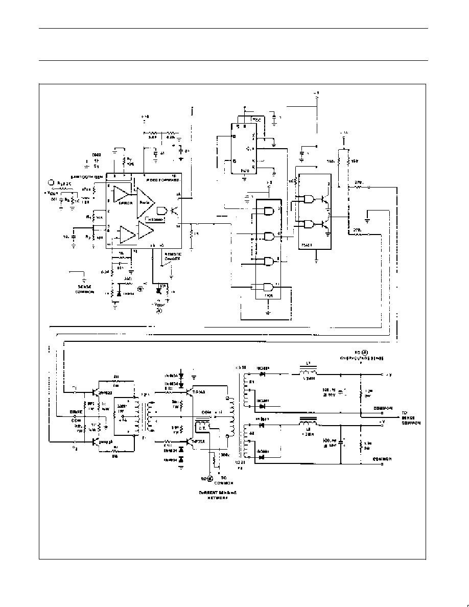
APPLICATIONS
NE/SE5560 Push-Pull Regulator
This application describes the use of the Philips Semiconductors
NE/SE5560 adapted to function as a push-pull switched mode
regulator, as shown in Figures 23 and 24.
Input voltage range is +12V to +18V for a nominal output of +30V
and -30V at a maximum load current of 1A with an average
efficiency of 81%.
Features include feed-forward input compensation, cycle-to-cycle
drive current protection and other voltage sensing, line (to positive
output) regulation <1% for an input range of +13V to +18V and load
regulation to positive output of <3% for
I
L
(+) of 0.1 to 1A.
The main pulse-width modulator operates to 48kHz with power
switching at 24kHz.
FEED-FORWARD
16
2
6
7
8
DO NOT EXCEED VCC
CSS
R1
R2
RT
CT
MAX
INPUT
SL00379
Figure 20. External
Maximum Control
WORKING
LEVEL
MAX
LEVEL
d
MAX
1
d
MAX
2
VZ
V16
2XVZ
T
T
SL00380
Figure 21. Feed-Forward Circuitry
DUTY
CYCLE
100
90
80
70
60
50
40
30
20
10
1
1.5
2
2.5
V
16
V
Z
SL00381
Figure 22. Feed-Forward Regulation

Philips Semiconductors
Product specification
NE/SE5560
Switched-mode power supply control circuit
1994 Aug 31
15
NOTES:
Power ground and signal ground must be kept separated
T1, Primary = 130T (C.T.) #26
Secondary = 18T (C.T.) #22
Core = Ferroxcube 3622
3C8 material
C.T. = 50T #26 0n
Ferroxcube 2616 core (3C8)
F2D bobbin
T2, Primary = 16T (C.T.) #18 Secondaries (each) 52T (C.T.) #22
Core = Ferroxcube 4229 3C8 material
L1, L2 = 120T #20 on single gapped EC35 Ferroxcube core. 3C8 material.
SL00382
Figure 23. NE/SE5560 Push-Pull Switched-Mode Regulated Supply with CMOS Drive Conversion Logic
Philips Semiconductors
Product specification
NE/SE5560
Switched-mode power supply control circuit
1994 Aug 31
16
NOTES:
Power ground and signal ground must be kept separated
T1, Primary = 130T (C.T.) #26
Secondary = 18T (C.T.) #22
Core = Ferroxcube 3622
3C8 material
C.T. = 50T #26 0n
Ferroxcube 2616 core (3C8)
F2D bobbin
T2, Primary = 16T (C.T.) #18 Secondaries (each) 52T (C.T.) #22
Core = Ferroxcube 4229 3C8 material
L1, L2 = 120T #20 on single gapped EC35 Ferroxcube core. 3C8 material.
SL00383
Figure 24. NE/SE5560 Push-Pull Switched-Mode Regulated With TTL Drive Conversion Logic