 | ÐлекÑÑоннÑй компоненÑ: NE57814 | СкаÑаÑÑ:  PDF PDF  ZIP ZIP |
Äîêóìåíòàöèÿ è îïèñàíèÿ www.docs.chipfind.ru

Philips
Semiconductors
NE57814
DDR memory termination regulator with
standby mode and enhanced efficiency
Product data
Supersedes data of 2003 Jan 22
2003 Apr 03
INTEGRATED CIRCUITS
Philips Semiconductors
Product data
NE57814
DDR memory termination regulator with
standby mode and enhanced efficiency
2
2003 Apr 03
DESCRIPTION
The NE57814 is designed to provide power for termination of a DDR
memory bus. It significantly reduces parts count, board space, and
overall system cost over previous switching solutions. The NE57814
has an independent power source pin (V
D
) for further reducing the
operational power and a standby low-power mode for
energy-sensitive portable applications.
The DDR terminator regulator provides a very accurate reference
(RefOut) and termination voltage (V
TT
) which is one-half of the RAM
supply voltage over wide range of current demand.
HSO8 (TOP)
HSO8 (BOTTOM)
FEATURES
·
Fast transient response time
·
Over-temperature protection
·
Over-current protection
·
Commercial (0
°
C to 70
°
C) temperature range
·
High bandwidth drivers minimize requirement for output hold-up
filter capacitors
·
Internal divider maintains termination voltage at
1
/
2
memory
supply voltage
·
RefOut output pin for other memory and control components
APPLICATIONS
·
Laptop computers
·
Desktop microcomputer systems
·
Workstations
·
Set-top boxes
·
Servers
·
Networking routers and switches
·
Video display systems
·
Personal video recorders
·
Game machines
·
Embedded systems
SIMPLIFIED SYSTEM DIAGRAM
DIMM0
DIMM1
Control & Address
Data
NE57814
RefOut
MEMORY
CONTROLLER
R
S
20
(typical)
R
T
27
(typical)
TERMINATION
POWER
V
TT
0.1
µ
F
100
µ
F
SL01877
V
TT
SENSE
V
D
V
DD
STANDBY
(OPTIONAL)
ExtRefIn
(OPTIONAL)
Figure 1. Simplified system diagram.
Philips Semiconductors
Product data
NE57814
DDR memory termination regulator with
standby mode and enhanced efficiency
2003 Apr 03
3
ORDERING INFORMATION
TYPE NUMBER
PACKAGE
TEMPERATURE
TYPE NUMBER
NAME
DESCRIPTION
VERSION
RANGE
NE57814DD
HSO8
plastic thermal enhanced small outline package; 8 leads;
body width 3.9 mm; exposed die pad
SOT786-2
0
°
C to +70
°
C
PIN CONFIGURATION
1
2
3
4
5
6
7
8
V
SS
V
TT
SENSE
V
TT
V
D
RefOut
STANDBY
ExtRefIn
V
DD
SL01878
Figure 2. Pin configuration.
PIN DESCRIPTION
PIN
SYMBOL
DESCRIPTION
1
V
SS
Terminator ground
2
V
TT
SENSE
V
TT
remote sense.
Connect to pin 3 (V
TT
)
3
V
TT
Terminator voltage output
4
V
D
V
TT
output MOSFET drain
5
V
DD
DDRAM supply voltage
6
ExtRefIn
Reference node used for external
control of V
TT
7
STANDBY
Places device into standby mode
(active-LOW)
8
RefOut
Buffered V
TT
reference output, used
for cascading terminators
NOTE:
1. The thermal heatspreader connects electrically to V
SS
internally
and provides enhancement to thermal conductivity, but it should
not be used as the primary connection to ground. Device
specifications apply to use of the V
SS
pin as the connection to
ground.
MAXIMUM RATINGS
SYMBOL
PARAMETER
MIN.
TYP.
MAX.
UNIT
V
DD
V
DD
to V
SS
voltage
0.3
+3.6
V
T
amb
Operating ambient temperature
0
+70
°
C
T
stg
Storage temperature
40
+165
°
C
T
j
Junction temperature
160
°
C
R
th(j-a)
Thermal resistance, junction to ambient (Note 1)
38.5
°
C/W
P
Power dissipation (Note 1)
2.1
W
NOTE:
1. Tested on a minimum footprint on a four-layer PCB per JEDEC specification JESD51-7.
Philips Semiconductors
Product data
NE57814
DDR memory termination regulator with
standby mode and enhanced efficiency
2003 Apr 03
4
ELECTRICAL CHARACTERISTICS
T
amb
= 0
°
C to +70
°
C; V
DD
= 2.5 V; V
D
= 2.5 V, unless otherwise specified.
SYMBOL
PARAMETER
CONDITIONS
MIN.
TYP.
MAX.
UNIT
V
TT
Output voltage
ExtRefIn not connected
V
DD
/2
V
Output voltage accuracy error
V
TT
V
DD
/2; I
TT
= 0 A
15
+15
mV
V
DD
Supply voltage
1.6
3.6
V
V
D
Supply voltage on pin V
D
1.6
3.6
V
I
Q(OP)
Operating supply current
I
TT
= 0 A
14
30
mA
I
TT
Output current (Note 5)
V
D
= V
DD
= 2.5 V to 3.6 V
3.5
+3.5
A
V
D
= V
DD
= 1.6 V
2.5
+2.5
A
I
Q(SD)
Standby quiescent current
Standby asserted
1.2
1.35
mA
V
TT
Load regulation
I
TT
=
±
1.0 A
±
6
mV
I
TT
=
±
3.5 A
18
+18
mV
C
LOAD
Min. load capacitance (Note 2)
Stable operation
50
100
µ
F
External Reference In
V
ExtRefIn
ExtRefIn voltage range
0.8
V
DD
0.8
V
R
in
ExtRefIn input impedance
35
50
k
V
ExtRefIn
V
TT
Output voltage accuracy
I
TT
= 0 A
15
+15
mV
Line regulation
V
ExtRefIn
= 1.25 V;
V
DD
= 2.25 V to 3.6 V
6
+6
mV
Reference Out
V
ERRREF
Voltage reference out (Note 4)
accuracy error, V
ExtRefIn
V
RefOut
I
RefOut
= 0 A
15
+15
mV
I
RefOut
Reference Out current limit
source or sink
2.2
3
mA
C
LOAD
Load capacitance
Stable operation
0.1
µ
F
Power Stage
I
lim
Current limit
3.6
4.5
6.5
A
R
ds(on)
Source transistor on-resistance
0.18
0.32
T
lim
Temperature shutdown
+150
°
C
Temperature shutdown hysteresis
20
°
C
NOTE:
1. Limits are 100% production tested at 25
°
C. Limits over the operating temperature range are guaranteed through correlation using Statistical
Quality Control (SQC) methods.
2. Ceramic capacitors. Low ESR Electrolytic capacitors are not required for stability, but may be needed for the application.
3. Voltage Accuracy referred to voltage at the center node of the V
ref
resistor divider.
4. RefOut voltage referenced to
1
/
2
V
DD
.
5. See Figure 15 for the Safe Operating Area versus Temperature.
Philips Semiconductors
Product data
NE57814
DDR memory termination regulator with
standby mode and enhanced efficiency
2003 Apr 03
5
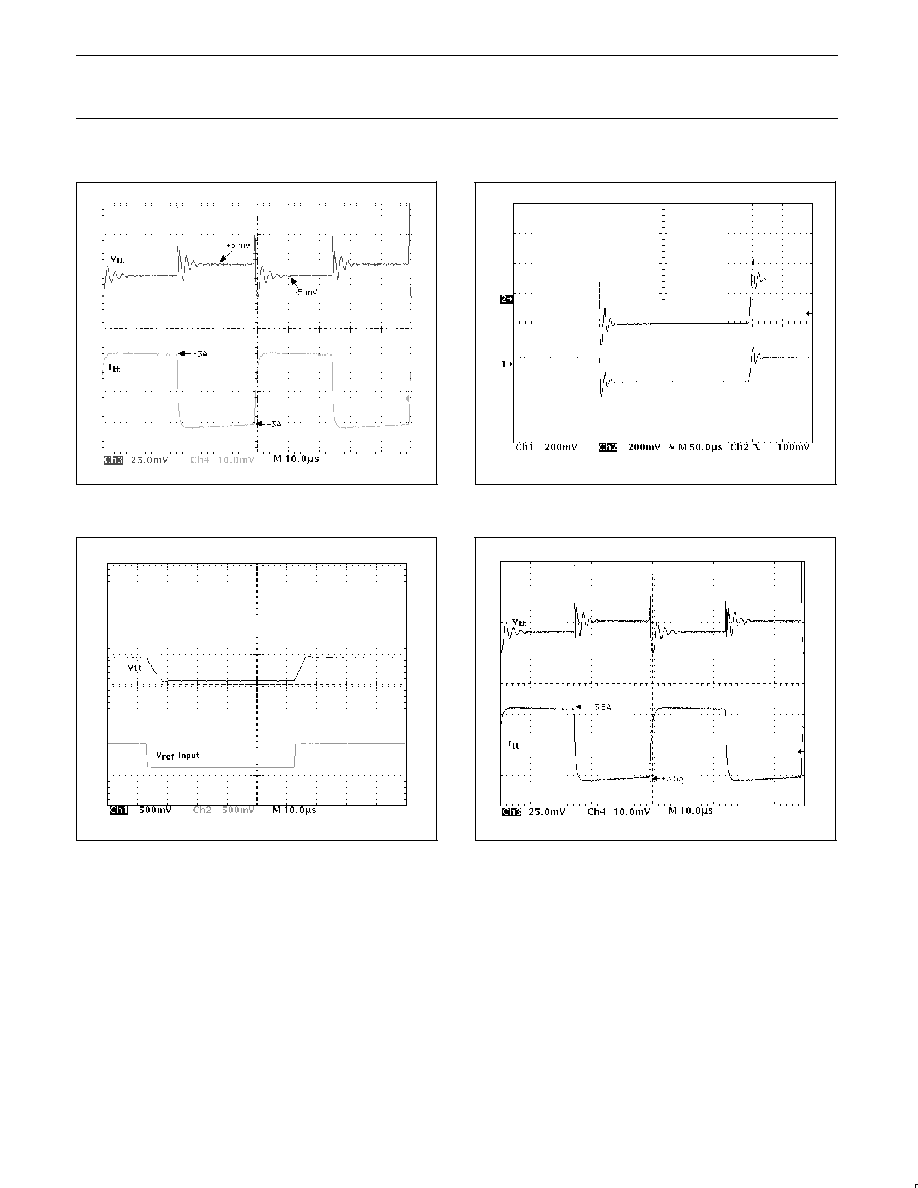
TYPICAL PERFORMANCE CURVES
SL01687
Figure 3. V
TT
transient response
(output filter 50
µ
F ceramic)
SL01688
Figure 4. V
DD
-to-V
TT
response
(output filter 50
µ
F ceramic)
SL01686
Figure 5. V
ref
-to-V
TT
transient response
(output filter 820
µ
F + 50
µ
F ceramic)
SL01685
Figure 6. V
ref
-to-V
TT
transient response
(output filter 50
µ
F ceramic)
Philips Semiconductors
Product data
NE57814
DDR memory termination regulator with
standby mode and enhanced efficiency
2003 Apr 03
6
1.200
1.210
1.220
1.230
1.240
1.250
1.260
1.270
1.280
1.290
1.300
6
5
4
3
2
1
0
1
2
3
4
5
6
Amps
V
olts
OUTPUT SINK
OUTPUT SOURCE
NORMAL OPERATING REGION
SL01684
Figure 7. Output regulation.
Philips Semiconductors
Product data
NE57814
DDR memory termination regulator with
standby mode and enhanced efficiency
2003 Apr 03
7
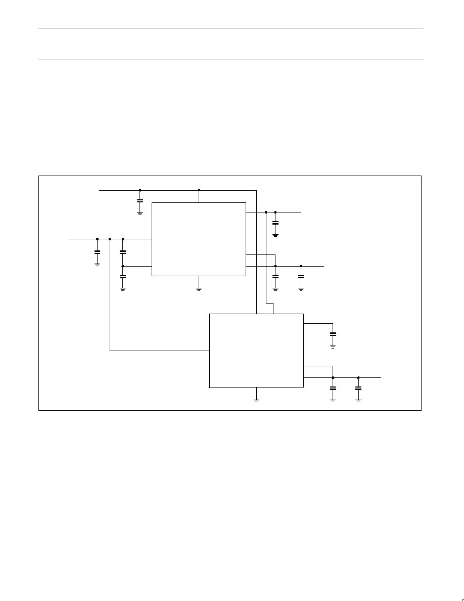
TECHNICAL DISCUSSION
The NE57814 supplies power to the DDR memory bus termination
resistors at one-half the voltage supplied to the memory ICs or
DIMMs. The DDR memory bus can only have one output drive any
one bus line at any one time. So the load on the DDR termination
system is a matter of the number of bus lines being terminated and
the termination resistor values. The memory size (that is the MB) of
memory space is not relevant. A typical DDR memory system is
seen in Figure 8. Each bus input/output pin on the bus has a series
20
resistor connected to it. The bus is terminated to the DDR
terminator though a 27 to 50
resistance. The memory system will
then require current from the terminator output only when the
instantaneous value of the aggregate bus does not correspond to
equal amounts of 1s and 0s. When memory bus speeds are in the
200300 MHz region, the period of any single bus state is extremely
small. This creates two bus loading conditions: the high frequency
condition which is caused by the instantaneous numbers of 1s and
0s, and the low frequency condition caused by mainly the address
bus being oriented towards the top or bottom of the memory space.
This creates two relatively independent output-filtering situations for
the DDR terminator: the high frequency bus speed, and the
low-frequency address skew of the processor system. Each should
be examined separately.
Figure 9 models the V
TT
loading condition of each bus line
equivalent circuit during operation and with terminating resistors.
This yields the worst case current loading equation:
I
O(max)
+
N
DDR
V
DD
2(
R
T
)
R
S
)
Where:
N
DDR
is the total number of terminated control, address and data
lines within the DDR memory system (typically 192).
R
T
is the value of the terminating resistors.
R
S
is the value of the series resistors from the active output
driver.
Hence the worst-case current loading condition for the typical DDR
memory is 194 terminated bus lines, and there are either all 1s or all
0s for an instant. If the terminator resistances are R
T
= 27
and
R
S
= 20
, then this results in a momentary instantaneous output
current of either + or 3.3 Amperes.
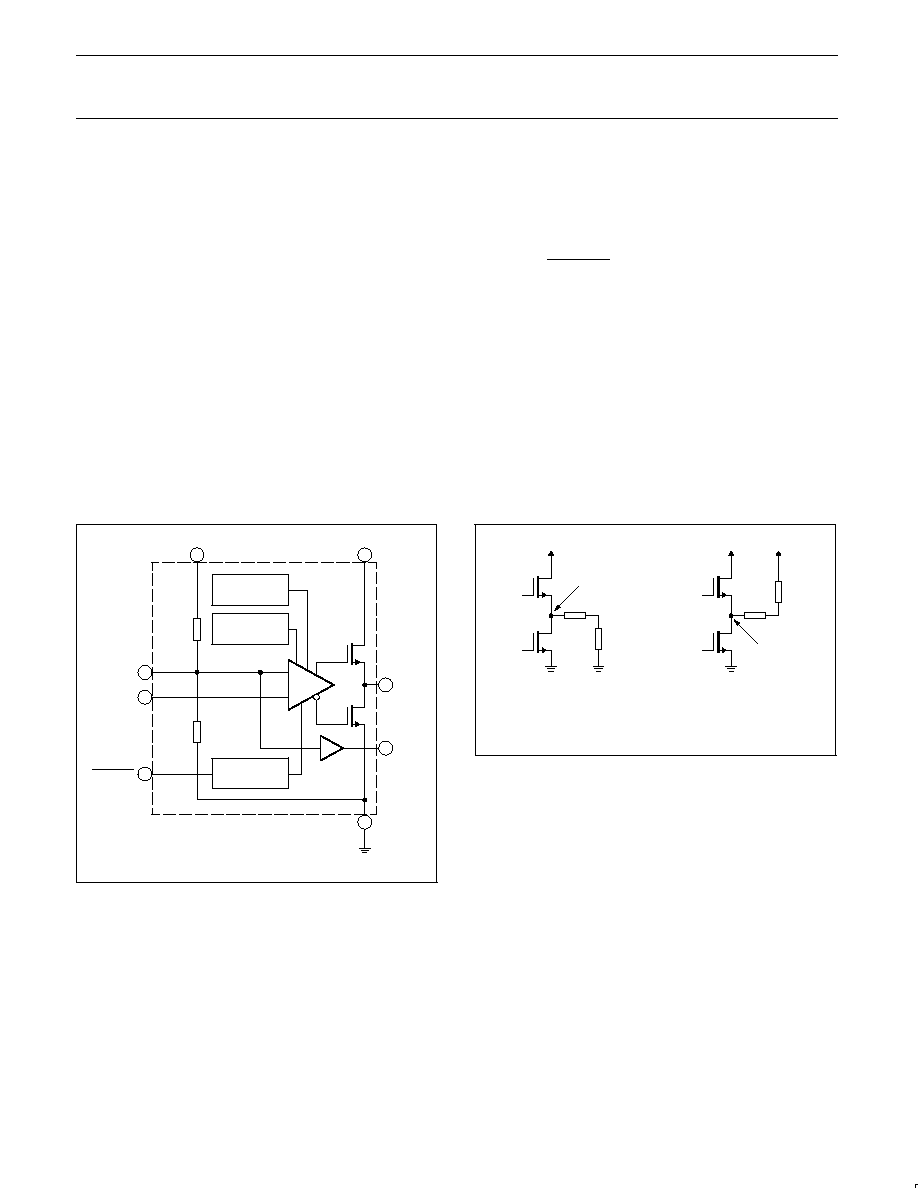
SL01879
V
TT
100 k
V
SS
ExtRefIn
OVERCURRENT
CONTROL
OVERTEMP
CONTROL
3
1
6
RefOut
8
4
V
D
5
V
DD
V
TT
SENSE
2
100 k
POWER
MANAGER
STANDBY 7
Figure 8. Functional diagram.
SL01880
V
D
V
D
V
DD
V
SS
V
SS
V
SS
V
TT
V
TT
R
T
R
S
R
T
R
S
A.
"1" DATA
B.
"0" DATA
Figure 9. The model for a single bus line for the DDR system.

Philips Semiconductors
Product data
NE57814
DDR memory termination regulator with
standby mode and enhanced efficiency
2003 Apr 03
8
APPLICATION INFORMATION
The NE57814 is intended for DDR memory termination systems
which require small space, low cost, high output transient current
dynamic range, and higher efficiency than the traditional linear DDR
terminator. The increased efficiency is gained by being able to draw
its output current from a lower voltage than the DDR RAM V
DD
voltage. As much as a 40 percent in the overall efficiency can be
gained by operating the output stage from a voltage source of
0.25 V above the output V
TT
voltage. This gives it a distinct benefit
in portable applications.
The standby mode turns OFF the V
TT
amplifier and 3-states the V
TT
output. The RefOut pin is still active for use elsewhere within the
system.
Using the STANDBY signal
The NE57814 provides a STANDBY pin that can be used to put the
device into low-power mode. When STANDBY is asserted (LOW),
the V
TT
power amplifier is turned off and the V
TT
output is 3-stated.
This brings the quiescent current of the entire device to less than
800
µ
A. The internal reference divider (ExtRefIn pin) and the
reference amplifier will remain active, allowing those circuits
requiring a reference during the STANDBY state to remain active.
If STANDBY is not externally connected, an internal 10 k
resistor
biases the control logic to V
DD
causing the output sections to be
turned on and the NE57814 operates normally.
Output filtering
There are two components to the memory signal load: a high
frequency component caused by the 266 MHz plus speed of the
address, data, and control buses, and a low frequency component
caused by the time-average skew of all of the bus states away from
an equal number of 1s and 0s. All electrolytic and tantalum
capacitors appear inductive at the high frequencies. Therefore two
types of capacitors are needed for the output filtering.
For a 256 MB memory space, for example, approximately 100
µ
F of
ceramic surface mount ceramic capacitors should be evenly
distributed across the physical memory layout. Depending upon the
PCB noise environment, this could be 10 pieces of 10
µ
F, 20 pieces
of 5
µ
F, and so on. These are the high frequency filter, represented
by C
out
(HF) in the illustrations. One half of the high frequency filter
capacitors should be connected to V
DD
and the other half to V
SS
so
that the output will better track any variations in the V
DD
voltage.
Filtering the lower frequencies of the DDR load usually requires
larger, low-ESR capacitors such as tantalum or low-ESR electrolytic
capacitors, shown as C
out
(LF) in the illustrations.
This is where the NE57814 excels. Because of its fast input and
output transient responses, very small or no additional large
capacitors are needed. Worst-case system analysis has shown that
an additional 110
µ
F of capacitance is needed for each microsecond
lag in the response time of the DDR regulator. The NE57814
responds in within one microsecond, so this requirement can be
filled by the 100
µ
F of ceramic capacitors already on the output.
Additional studies have shown that other regulators, which cannot
directly source the maximum instantaneous current demanded from
the termination system, must have an additional 75
µ
F of
capacitance for each ampere of insufficient output drive.
Together, the fast output response and peak drive current
capabilities make the NE57814 the ideal choice for DDR
termination.
Philips Semiconductors
Product data
NE57814
DDR memory termination regulator with
standby mode and enhanced efficiency
2003 Apr 03
9
High efficiency operating mode
The NE57814 is designed for portable applications such as laptop
computers and other battery operated computer systems requiring
DDR memory. The standby mode 3-states the V
TT
output and
unpowers most of the NE57814, which is very desirable for portable
applications. The RefOut pin is still active for use elsewhere within
the system.
The V
D
pin on the NE57814 allows the DDR termination system to
operate with reduced output power dissipation. The V
D
voltage can
be lowered to approximately +0.25 volts above the V
TT
output
voltage.
The high-efficiency method draws its V
TT
current, not from the
memory V
DD
line but from a lower voltage, V
D
. This will decrease
the loss within the terminator when it sources current to the V
TT
line.
The V
D
voltage required depends on the load current sourced and is
given by V
D(min)
= V
TT
+ 0.3(I
TT(source)
). I
TT
is expressed in amps.
The V
DD
voltage is still used to set the V
ref
voltage to the memory
devices.
As much as a 65 percent overall efficiency can be gained by
operating the output stage from a voltage source of 0.25 V above
the output V
TT
voltage during the sourcing condition. This gives it a
distinct benefit in portable applications.
The efficiency of the DDR terminator during the sourcing and sinking
states of the NE57814 can be determined by the following
calculations:
Sourcing:
Efficiency(sourcing)
+
(
V
TT
) (
I
TT
)
(
I
Q
) (
V
DD
)
)
(
V
D
*
V
TT
) (
I
TT
)
100
This can be between 81 and 82.5 percent when the NE57814 is
sourcing current.
Sinking:
Efficiency(sinking)
+
(
V
TT
) (
I
TT
)
(
I
Q
) (
V
DD
)
)
(
V
TT
) (
I
TT
)
100
This is approximately 49.5 percent.
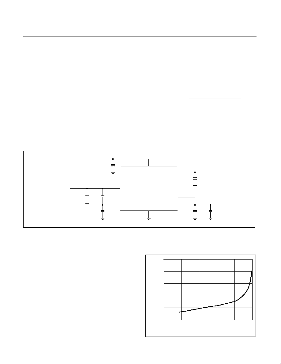
SL01884
V
DD
5
ExtRefIn
6
V
SS
1
V
TT
3
V
TT
SENSE
2
RefOut
8
V
D
4
V
ref
V
TT
50
µ
F
(Y5V)
0.1
µ
F
(Y5V)
NE57814
470
µ
F
(Electro)
0.1
µ
F
(Y5V)
0.1
µ
F
(Y5V)
INPUT VOLTAGE
( > V
TT
+ 0.25 V )
10
µ
F
(Y5V)
V
DD
VOLTAGE
Figure 10. High efficiency operation.
Less than +0.25 V between V
D
and V
TT
A voltage difference between V
D
and V
TT
of less than +0.25 V
reduces the maximum sourcing current capability of the V
TT
power
amplifier.
This reduction in output sourcing current capability can many times
be compensated for within the termination system by adding
additional low ESR electrolytic capacitors on the V
TT
output. The
typical performance of the NE57814 as the V
D
voltage approaches
V
TT
voltage (decreasing headroom voltage) can be seen in
Figure 11.
TERMINA
TION
CURRENT
(A), I
TT
SL01885
HEADROOM VOLTAGE (mV)
0
50
100
150
200
250
2.5
2.0
1.5
1.0
0.5
0
Figure 11. Typical output source current versus V
D
(at 25
°
C).
Philips Semiconductors
Product data
NE57814
DDR memory termination regulator with
standby mode and enhanced efficiency
2003 Apr 03
10
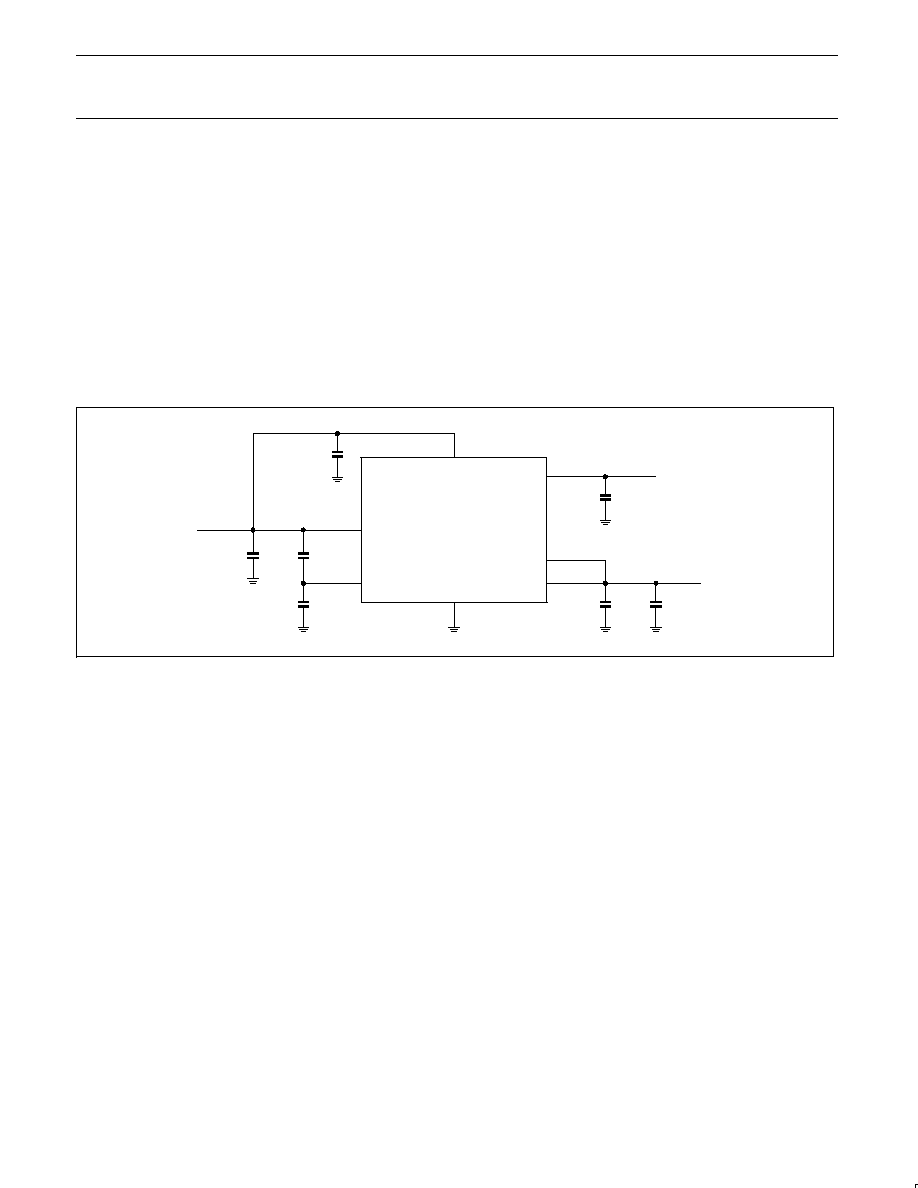
Single-supply operating mode (V
DD
supply only)
For single-supply operation, connect the V
D
pin to the V
DD
pin. This
is suitable for use in a desktop computer or other non
efficiency-sensitive application (see Figure 12).
Externally setting V
TT
The NE57814 allows use of an external reference voltage applied to
the ExtRefIn pin to set the V
TT
output voltage. This pin is used for
applications where the V
TT
voltage is not equal to V
DD
divided by 2.
The needed V
TT
voltage and current may be drawn from a power
supply bus that is not the DDR RAM supply voltage. This may have
some advantages when the system designer is attempting to better
match the power being drawn from the outputs emerging from main
system power supply.
The internal reference voltage is set by two matched 100 k
resistors connected in a resistor divider between the V
DD
and Vss
pins of the NE57814. Setting the value of V
ref
or V
TT
can be done in
two ways: by using an external resistor divider whose resistor values
are less than 5 k
each or by connecting the output of an
operational amplifier which is outputting the reference voltage to the
ExtRefIn pin.
If the external resistor divider is used, place a 0.01
µ
F ceramic
bypass capacitor between the ExtRefIn pin (pin 6) and the V
SS
pin
(pin 1). The accuracy of the new reference voltage when the
external resistor divider is used will be about 0.5 percent PLUS the
sum of the tolerances of the resistors used in the divider.
Please note that when the NE57814 is operating in this fashion, the
power dissipation of the part may increase.
SL01886
V
DD
5
ExtRefIn
6
V
SS
1
V
TT
3
V
TT
SENSE
2
RefOut
8
V
D
4
50
µ
F
(Y5V)
0.1
µ
F
(Y5V)
NE57814
470
µ
F
(Electro)
0.1
µ
F
(Y5V)
0.1
µ
F
(Y5V)
10
µ
F
(Y5V)
100
µ
F
(Electro)
Figure 12. Single-supply operation.
Philips Semiconductors
Product data
NE57814
DDR memory termination regulator with
standby mode and enhanced efficiency
2003 Apr 03
11
Cascading the NE57814 for complex memory
systems
For high-performance computer systems, such as workstations and
servers, where two or more banks of independent memory arrays
are needed, the NE57814 can be cascaded to provide two
independent, but slaved termination systems. This type of
architecture allows the termination voltages to be within 12 mV of
one another, and the V
TT
can be controlled from a single node.
Cascading NE57814 terminators offers two advantages; memory
SIMMs can be brought closer to the terminator, which improves the
system noise, and it will better distribute any heat generated by the
terminator system. Use the RefOut pin from one NE57814 to the
ExtRefIn pin for the other NE57814(s) in the system to ensure that
the V
TT
voltages are identical.
The output of the NE57814 is a very low impedance voltage source
which means that the V
TT
outputs should never be wired together.
That is, NE57814s should never be wired in parallel. This is
because the terminators would "fight" one another if their output
were different by only a few millivolts.
The cascading method can be seen in Figure 13.
SL01887
V
DD
ExtRefIn
V
SS
V
TT
V
TT
SENSE
RefOut
V
D
V
ref
V
TT
50
µ
F
(Y5V)
0.1
µ
F
(Y5V)
NE57814
470
µ
F
(Electro)
0.1
µ
F
(Y5V)
0.1
µ
F
(Y5V)
INPUT VOLTAGE
( > V
TT
+ 0.25 V )
10
µ
F
(Y5V)
100
µ
F
(Electro)
V
DD
ExtRefIn
V
SS
V
TT
V
TT
SENSE
RefOut
V
D
50
µ
F
(Y5V)
0.1
µ
F
(Y5V)
NE57814
INPUT VOLTAGE
( > V
TT
+ 0.25 V )
Figure 13. Cascading terminator systems for complex memory systems.
Philips Semiconductors
Product data
NE57814
DDR memory termination regulator with
standby mode and enhanced efficiency
2003 Apr 03
12
THERMAL DESIGN
Designing the thermal system for the NE57814 is important for its
reliable operation. The NE57814 will be operating at an average
power level less than the maximum rating of the part. In a typical
DDR terminator system the average power dissipation is between
0.8 and 1.5 watts. It is important to make sure that this average
power dissipation is less than the power capability of the package.
The terminator heatsink must be designed to accommodate the
average power as a steady state condition and be able to withstand
momentary periods of increased dissipation, say from 12 seconds.
For the single-supply application, the power dissipated by the
terminator can be calculated:
P
D
+
I
DD
V
TT
Watts
Eqn. (1)
The thermal resistance of a surface mount package is given as
R
th(j-a)
(thermal resistance from the junction to air). JESD51-7
specifies a 4-layer PCB (2oz/1oz/1oz/2oz copper) that is 4 inches on
each side. This is probably the best (or lowest thermal resistance)
one will see in any application. Most applications cannot afford the
PCB area to create this situation, but the thermal performance of a
multi-layer PCB will still provide a significant heat sinking effect. The
actual thermal resistance will be higher than the 38.5
°
C/W given for
the 4-layer JEDEC PCB.
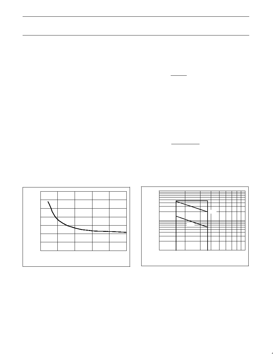
Figure 14 shows what thermal resistance one can expect for heat
sinking PCB areas less than the JEDEC specification. The
resistance can be decreased by using a double-sided PCB with
some plated through holes (vias) to help transfer the heat to the
bottom side. The thermal resistance decreases by about 34
°
C/W
for a double-sided board with vias.
THERMAL
RESIST
ANCE ( C/W)
°
SL01888
LENGTH OF SIDE OF 2 oz. COPPER AREA (mm)
0
20
40
60
80
100
55
50
45
40
35
30
25
60
Figure 14. Thermal resistance versus PCB area.
After the power is estimated, the minimum PCB area can be
determined by calculating the worst-case thermal resistance and
referring to Figure 8 to determine the PCB area. This is done by:
R
th(j-a)(min)
+
T
j
*
T
amb
P
Eqn. (2)
Where:
T
j
is the maximum desired junction temperature.
T
amb
is the highest expected local ambient temperature.
P is the estimated average power
The junction temperature should be kept below the
over-temperature cutoff threshold temperature (+140
°
C ) in normal
operation.
Using the power dissipation formula above, the highest ambient
temperature, 1.5 watts power dissipation (used only as an example)
and a junction temperature of +125
°
C, calculate the maximum
thermal resistance as follows:
R
th(ja)(min)
+
140
O
C
*
70
O
C
1.5
W
+
47
O
C W
Eqn. (3)
Looking at Figure 15, a minimum PCB island area of 225 mm
2
(15 mm length and width) is required at this power dissipation. Of
course, increasing this area will allow the NE57814 to operate at
cooler temperatures, enhancing the long-term reliability and allowing
the terminator to better handle any transient output current
demands.
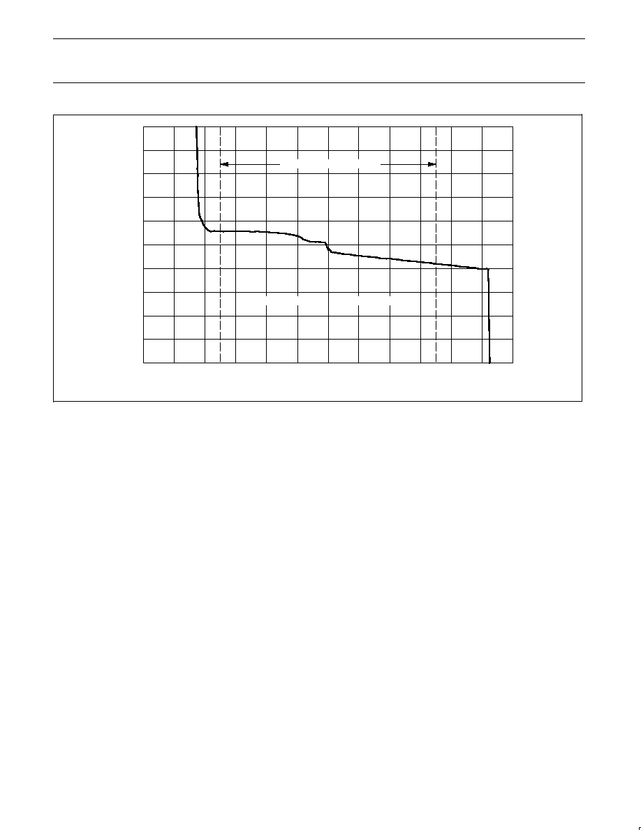
I (A)
DD
SL01873
V
DD
(V)
1
2
3
4
5
6
1
0.1
10
DC
0.5 s
7
8
9 10
Figure 15. Safe operating area of the NE57814.
Philips Semiconductors
Product data
NE57814
DDR memory termination regulator with
standby mode and enhanced efficiency
2003 Apr 03
13
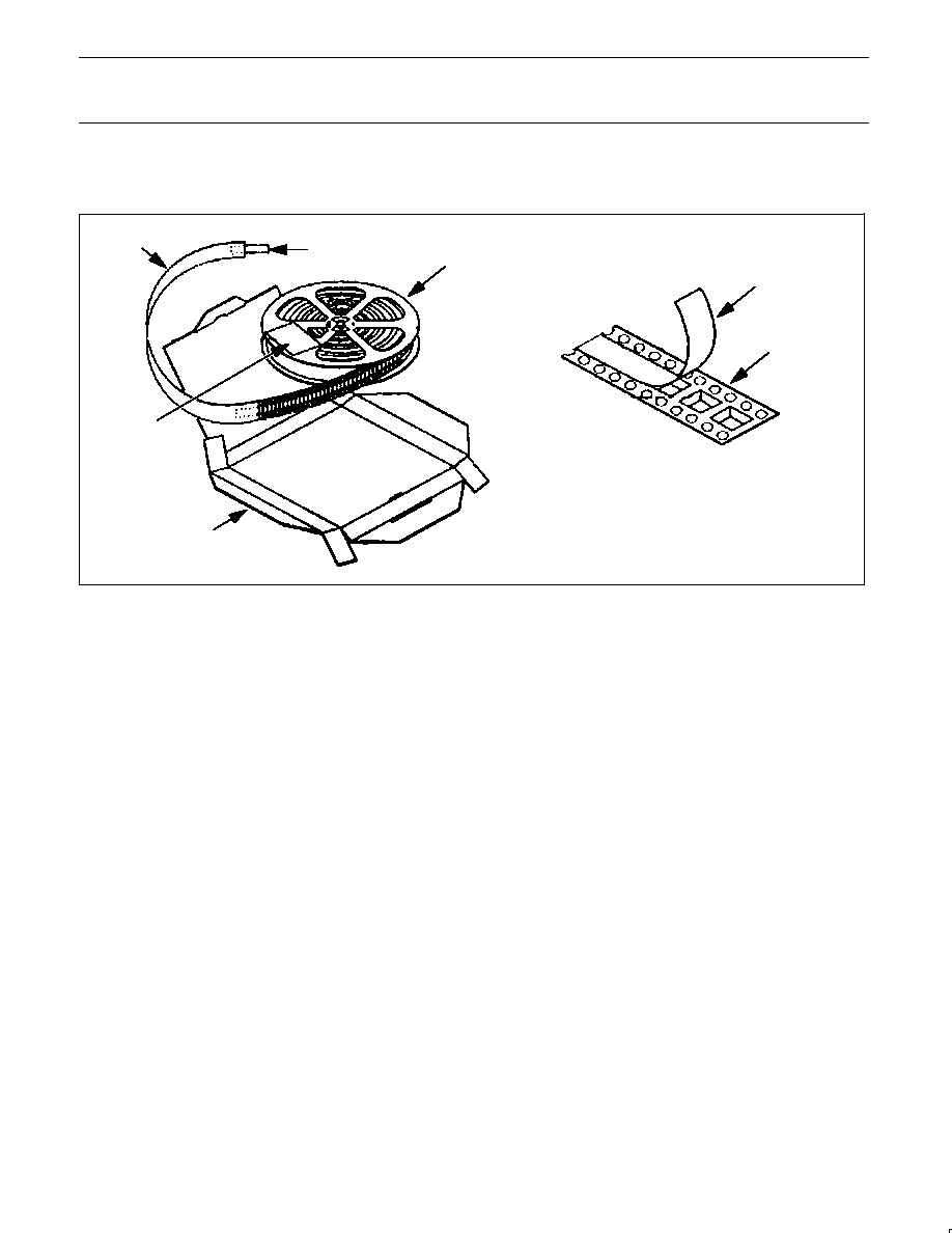
PACKING METHOD
The NE57814 is packed in reels, as shown in Figure 16.
SL01305
TAPE DETAIL
COVER TAPE
CARRIER TAPE
REEL
ASSEMBLY
TAPE
GUARD
BAND
BARCODE
LABEL
BOX
Figure 16. Tape and reel packing method.
Philips Semiconductors
Product data
NE57814
DDR memory termination regulator with
standby mode and enhanced efficiency
2003 Apr 03
14
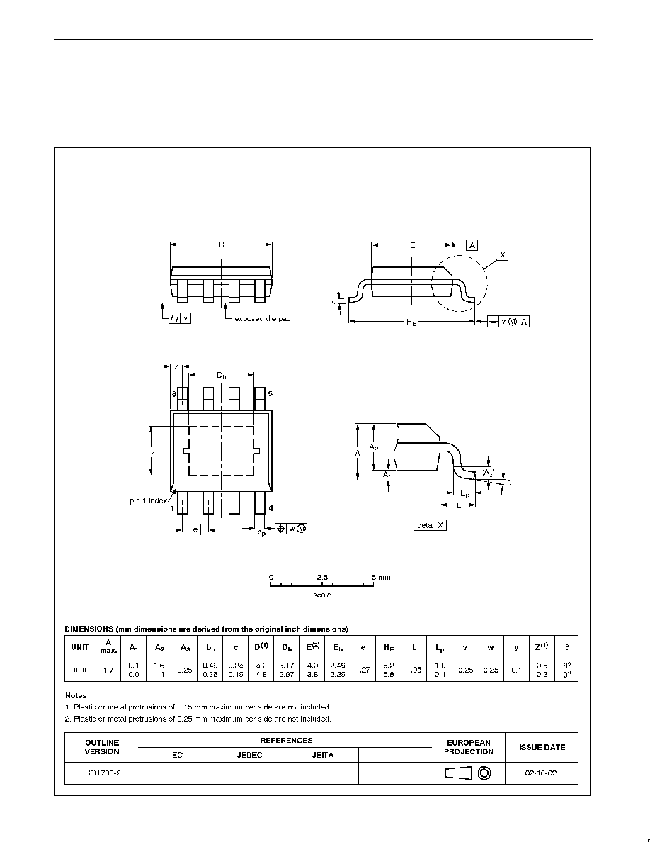
HSO8:
plastic thermal enhnaced small outline package;
8 leads; body width 3.9 mm; exposed die pad
SOT786-2
Philips Semiconductors
Product data
NE57814
DDR memory termination regulator with
standby mode and enhanced efficiency
2003 Apr 03
15
REVISION HISTORY
Rev
Date
Description
_3
20030403
Product data (9397 750 11217); ECN 853-2399 29610 of 03 March 2003;
supersedes data of 2003 Jan 22 (9397 750 10984).
Modifications:
·
Description on page 2, second paragraph: delete second sentence.
·
Electrical Characteristics table on page 4:
Symbol I
Q(OP)
: change Typ. value from 20 mA to 14 mA.
Symbol I
Q(SD)
: change Typ. value from () to 1.2 mA.
Add new Note 1, and renumber following notes and their references.
_2
20030122
Product data (9397 750 10984); ECN 853-2399 29323 dated 2002 Dec 19;
supersedes Objective data of 2002 Nov 07 (9397 750 10618).
_1
20021107
Objective data; initial version (9397 750 10618).

Philips Semiconductors
Product data
NE57814
DDR memory termination regulator with
standby mode and enhanced efficiency
2003 Apr 03
16
Definitions
Short-form specification -- The data in a short-form specification is extracted from a full data sheet with the same type number and title. For detailed information see
the relevant data sheet or data handbook.
Limiting values definition -- Limiting values given are in accordance with the Absolute Maximum Rating System (IEC 60134). Stress above one or more of the limiting
values may cause permanent damage to the device. These are stress ratings only and operation of the device at these or at any other conditions above those given
in the Characteristics sections of the specification is not implied. Exposure to limiting values for extended periods may affect device reliability.
Application information -- Applications that are described herein for any of these products are for illustrative purposes only. Philips Semiconductors make no
representation or warranty that such applications will be suitable for the specified use without further testing or modification.
Disclaimers
Life support -- These products are not designed for use in life support appliances, devices, or systems where malfunction of these products can reasonably be
expected to result in personal injury. Philips Semiconductors customers using or selling these products for use in such applications do so at their own risk and agree
to fully indemnify Philips Semiconductors for any damages resulting from such application.
Right to make changes -- Philips Semiconductors reserves the right to make changes in the products--including circuits, standard cells, and/or software--described
or contained herein in order to improve design and/or performance. When the product is in full production (status `Production'), relevant changes will be communicated
via a Customer Product/Process Change Notification (CPCN). Philips Semiconductors assumes no responsibility or liability for the use of any of these products, conveys
no license or title under any patent, copyright, or mask work right to these products, and makes no representations or warranties that these products are free from patent,
copyright, or mask work right infringement, unless otherwise specified.
Contact information
For additional information please visit
http://www.semiconductors.philips.com.
Fax: +31 40 27 24825
For sales offices addresses send e-mail to:
sales.addresses@www.semiconductors.philips.com.
©
Koninklijke Philips Electronics N.V. 2003
All rights reserved. Printed in U.S.A.
Date of release: 04-03
Document order number:
9397 750 11217
Philips
Semiconductors
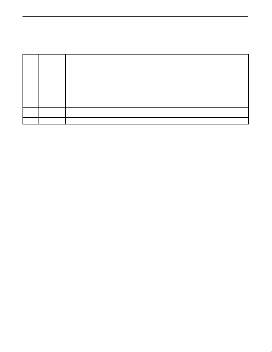
Data sheet status
[1]
Objective data
Preliminary data
Product data
Product
status
[2] [3]
Development
Qualification
Production
Definitions
This data sheet contains data from the objective specification for product development.
Philips Semiconductors reserves the right to change the specification in any manner without notice.
This data sheet contains data from the preliminary specification. Supplementary data will be published
at a later date. Philips Semiconductors reserves the right to change the specification without notice, in
order to improve the design and supply the best possible product.
This data sheet contains data from the product specification. Philips Semiconductors reserves the
right to make changes at any time in order to improve the design, manufacturing and supply. Relevant
changes will be communicated via a Customer Product/Process Change Notification (CPCN).
Data sheet status
[1] Please consult the most recently issued data sheet before initiating or completing a design.
[2] The product status of the device(s) described in this data sheet may have changed since this data sheet was published. The latest information is available on the Internet at URL
http://www.semiconductors.philips.com.
[3] For data sheets describing multiple type numbers, the highest-level product status determines the data sheet status.
Level
I
II
III
Document Outline
- DESCRIPTION
- FEATURES
- APPLICATIONS
- SIMPLIFIED SYSTEM DIAGRAM
- ORDERING INFORMATION
- PIN CONFIGURATION
- PIN DESCRIPTION
- MAXIMUM RATINGS
- ELECTRICAL CHARACTERISTICS
- TYPICAL PERFORMANCE CURVES
- TECHNICAL DISCUSSION
- APPLICATION INFORMATION
- THERMAL DESIGN
- PACKING METHOD
- PACKAGE OUTLINE
- REVISION HISTORY
- Data sheet status
- Definitions
- Disclaimers