 | –≠–ª–µ–∫—Ç—Ä–æ–Ω–Ω—ã–π –∫–æ–º–ø–æ–Ω–µ–Ω—Ç: NE600D | –°–∫–∞—á–∞—Ç—å:  PDF PDF  ZIP ZIP |


Philips Semiconductors
Product specification
NE/SA600
1GHz LNA and mixer
1993 Dec 15
49
AC ELECTRICAL CHARACTERISTICS
1,2
SYMBOL
PARAMETER
TEST CONDITIONS
LIMITS
UNITS
SYMBOL
PARAMETER
TEST CONDITIONS
≠3
TYP
+3
UNITS
LNA (V
CC
= V
CCMX
= +5V, T
A
= 25
∞
C; Enable = Hi, Test Figure 1, unless otherwise stated.)
S
21
Amplifier gain
900MHz
14.9
16
17.1
dB
S
21
Amplifier gain in thru mode
Enable = LO, 900MHz
≠9.0
-7.5
≠6.0
dB
S
21
/
T
Gain temperature sensitivity enabled
900MHz
-0.008
dB/
∞
C
S
21
/
T
Gain temperature sensitivity in thru mode
Enable = LO, 900MHz
-0.014
dB/
∞
C
S
21
/
f
Gain frequency variation
800MHz - 1.2GHz
-0.014
dB/MHz
S
12
Amplifier reverse isolation
900MHz
≠47
-42
≠37
dB
S
11
Amplifier input match
3
900MHz
≠11
-10
≠9
dB
S
22
Amplifier output match
900MHz
≠16.8
-15
≠13.2
dB
P
-1dB
Amplifier input 1dB gain compression
900MHz
≠21.2
-20
≠18.8
dBm
IP
3
Amp input 3rd-order intercept
Test Fig. 2, 900MHz
≠11.6
-10
≠8.6
dBm
Amp input 3rd-order intercept (thru mode)
Test Fig. 2, 900MHz, Enable = LO
+26
dBm
Amplifier noise figure
900MHz
1.9
2.2
2.5
dB
NF
Amp noise figure w/shunt 15nH inductor
at input
900MHz
1.7
2.0
2.3
dB
t
ON
Amplifier turn-on time
Coupling = 100pF
Coupling = 0.01
µ
F
Enable Lo
Hi
30
3
µ
s
ms
t
OFF
Amplifier turn-off time
Coupling = 100pF
Coupling = 0.01
µ
F
Enable Hi
Lo
10
1
µ
s
ms
Mixer (V
CC
= V
CCMX
= +5V, T
A
= 25
∞
C, Enable = Hi, f
LO
= 1GHz @ 0dBm, f
RF
= 900MHz, f
IF
= 100MHz, Test Fig. 1, unless otherwise stated)
VG
C
Mixer voltage conversion gain
R
L1
= R
L2
= 1k
9.5
10.4
11.3
dB
PG
C
Mixer power conversion gain
R
L1
= R
L2
= 1k
≠3.05
≠2.6
≠2.15
dB
S
11RF
Mixer input match
900MHz
≠23
-20
≠17
dB
NF
M
Mixer SSB noise figure
Test Fig. 3, 900MHz, f
IF
= 80MHz
12.2
14
15.8
dB
P
-1dB
Mixer input 1dB gain compression
900MHz
≠5.3
-4
≠2.7
dBm
IP
3INT
Mixer input third order intercept
900MHz
+5
+6
+7
dBm
IP
2INT
Mixer input second order intercept
900MHz
+18
+20
+22
dBm
G
RFM-IF
Mixer RF feedthrough
900MHz, C
IF
= 3pF
≠7
dB
G
LO-IF
Mixer LO feedthrough
900MHz, C
IF
= 3pF
-10
dB
G
LO-RFM
Local oscillator to mixer input feedthrough
900MHz
-33
dB
S
11LO
LO input match
900MHz
≠24
≠20
≠16
dB
G
LO-RF
Local oscillator to RF input feedthrough
900MHz
-46
dB
G
RFO-RFM
Filter feedthrough
900MHz
-39
dB
LNA + Mixer (V
CC
=V
CCMX
=+5V, T
A
=25
∞
C, Enable=Hi, f
LO
=1GHz @ 0dBm, f
RF
= 900MHz, f
IF
= 100MHz, Test Fig. 1, unless otherwise
stated)
PG
C
Overall power conversion gain
13.4
dB
NF
Overall noise figure
3.5
dB
IP
3
Overall input 3rd-order intercept
≠13
dBm
NOTE:
1. All meausrements include the effects of the NE/SA600 Evaluation Board (see Figure ) unless otherwise noted. Measurement system
impedance is 50
.
2. Standard deviations are estimated from design simulations to represent manufacturing variations over the life of the product.
3. With a shunt 15nH inductor at the input of the LNA, the value of S
11
is typically ≠15dB.

Philips Semiconductors
Product specification
NE/SA600
1GHz LNA and mixer
1993 Dec 15
50
14
13
12
11
4
3
2
1
NE/SA600
10
9
8
7
6
5
IMAGE
REJECTION
FILTER
POWER-DOWN
CONTROL
LO INPUT
0dBm
1.0GHz
BYPASS
RF
INPUT
900MHz
+5V
0.01
µ
F
100pF
0.1
µ
F
RF IN MX
RF OUT A
IF OUT
RFC
10
µ
H
1k
100pF
NOTES:
RATIO OF BYPASS TO SIGNAL COUPLING CAPS FOR LNA SHOULD BE 100:1
OR GREATER.
IF FILTER SHOULD BE AC COUPLED.
1k
IF FILTER
100MHz
RL2
RL1
14
13
12
11
4
3
2
1
NE/SA600
10
9
8
7
6
5
POWER-DOWN
CONTROL
LO INPUT
0dBm
1.0GHz
BYPASS
RF
INPUT
900MHz
+5V
RFC
1
µ
F
0.01
µ
F
0.1
µ
F
RF IN MX
RF OUT A
IF OUT
10
µ
H
50
0.01
µ
F
0.01
µ
F
0.01
µ
F
14
13
12
11
4
3
2
1
NE/SA600
10
9
8
7
6
5
POWER-DOWN
CONTROL
LO INPUT
0dBm
1.0GHz
BYPASS
RF
INPUT
900MHz
+5V
RFC
0.01
µ
F
100pF
0.1
µ
F
RF IN MX
RF OUT A
IF OUT
10
µ
H
1k
100pF
100pF
100pF
50
RL1
4.7pF
470nH
14
13
12
11
4
3
2
1
NE/SA600
10
9
8
7
6
5
IMAGE
REJECTION
FILTER
POWER-DOWN
CONTROL
LO INPUT
0dBm
1.0GHz
BYPASS
RF
INPUT
900MHz
+5V
RFC
1
µ
F
0.1
µ
F
RF IN MX
RF OUT A
10
µ
H
1k
RL1
0.01
µ
F
0.01
µ
F
0.01
µ
F
0.01
µ
F
IF OUT
50
4.7pF
470nH
TYPICAL APPLICATION
TEST FIGURE 1
TEST FIGURE 2
TEST FIGURE 3
0.01
µ
F
0.01
µ
F
0.01
µ
F
SR00084
Figure 3. Test Application and Test Figures 1, 2 and 3

Philips Semiconductors
Product specification
NE/SA600
1GHz LNA and mixer
1993 Dec 15
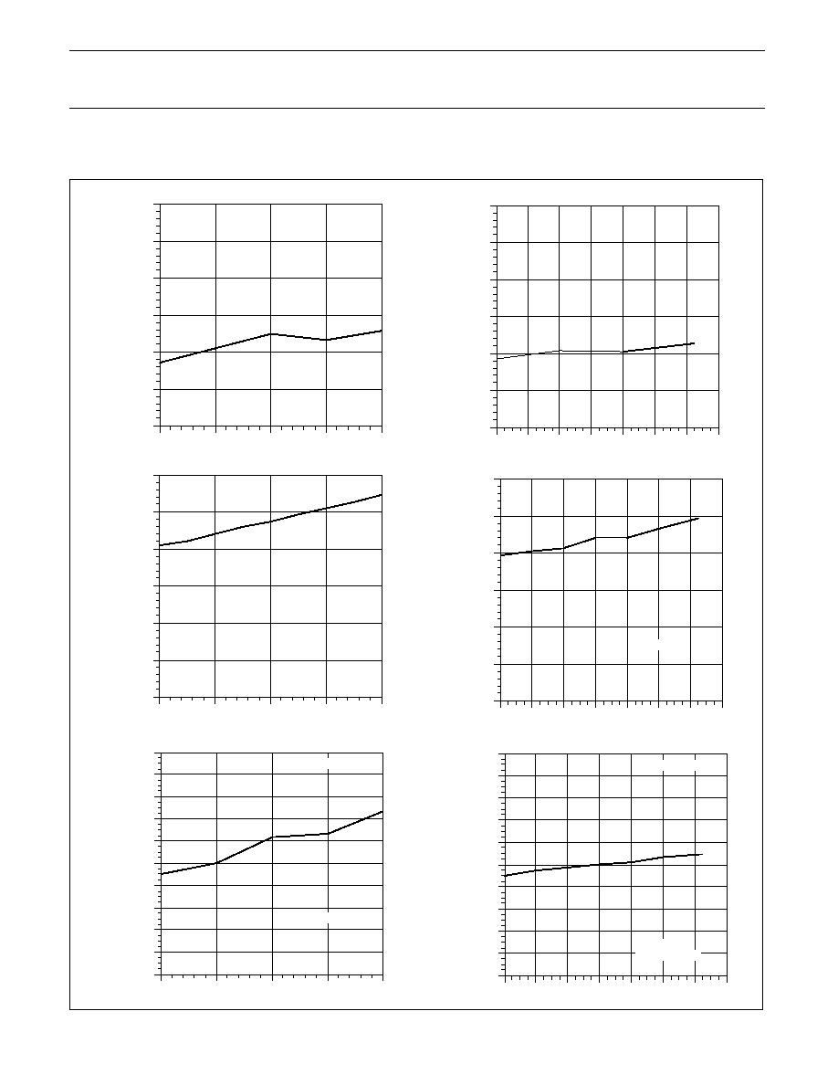
51
NOTE: All performance curves include the effects of the NE/SA600 evaluation board.
LNA S21 CHARACTERISTICS
4.5V
V
CC
= V
CCMX
5.5V, Test Figure 1, unless otherwise specified.
LNA S21 vs Frequency
40
30
20
10
0
≠10
≠20
10
100
1000
2000
FREQUENCY (MHz)
S21 MAGNITUDE (dB)
ENABLE=HI
ENABLE=LO
LNA S21 vs Frequency
20
15
10
5
0
≠5
≠10
800
900
1000
1100
1200
S21 MAGNITUDE (dB)
FREQUENCY (MHz)
ENABLE=HI
ENABLE=LO
LNA S21 Phase vs Frequency
0
800
S21 PHASE (Deg)
FREQUENCY (MHz)
900
1000
1100
1200
≠20
≠40
≠60
≠80
≠100
≠120
S21 MAGNITUDE (dB)
FREQUENCY (MHz)
LNA S21 vs Frequency and V
CC
800
900
1000
18
17.5
17
16.5
16
15.5
15
VCC = 4.5V
VCC = 5.0V
VCC = 5.5V
≠40
∞
C
800
FREQUENCY (MHz)
LNA S21 vs Frequency and Temperature
20
S21 MAGNITUDE (dB)
18
16
14
12
10
8
6
4
2
0
900
1000
1100
1200
25
∞
C
85
∞
C
≠40
∞
C
800
FREQUENCY (MHz)
LNA Thru S21 vs Frequency and Temperature
0
S21 MAGNITUDE (dB)
900
1000
1100
1200
25
∞
C
85
∞
C
≠2
≠4
≠6
≠8
≠10
≠12
SR00085
Figure 4. LNA S21 Performance Characteristics

Philips Semiconductors
Product specification
NE/SA600
1GHz LNA and mixer
1993 Dec 15
52
LNA S11/S12/S22 CHARACTERISTICS
4.5V
V
CC
= V
CCMX
5.5V, Test Figure 1, unless otherwise specified.
≠40
∞
C
800
FREQUENCY (MHz)
LNA S11 vs Frequency and Temperature
0
S1
1 MAGNITUDE (dB)
900
1000
1100
1200
25
∞
C
85
∞
C
≠2
≠4
≠6
≠8
≠10
≠12
≠14
≠16
≠18
≠20
LNA S12 vs Frequency
0
10
100
1000
2000
FREQUENCY (MHz)
S12 MAGNITUDE (dB)
ENABLE=HI
≠10
≠20
≠30
≠40
≠50
≠60
≠70
≠80
≠40
∞
C
800
FREQUENCY (MHz)
LNA S22 vs Frequency and Temperature
0
S22 MAGNITUDE (dB)
900
1000
1100
1200
25
∞
C
85
∞
C
≠2
≠4
≠6
≠8
≠10
≠12
≠14
≠16
≠18
≠20
S22
800
FREQUENCY (MHz)
LNA Thru S11 and S22 vs Frequency
0
Sii MAGNITUDE (dB)
900
1000
1100
1200
≠2
≠4
≠6
≠8
≠10
≠12
≠14
≠16
≠18
≠20
S11
SR00086
Figure 5. LNA S11/S12/S22 Performance Characteristics
Table 1.
S-Parameters
Freq. MHz
S
11
S
12
S
21
S
22
800
-9.5
-160
-46
8
17.9
125
-18.0
151
900
-9.5
-172
-43
19
16.4
105
-15.8
122
1000
-9.4
-173
-40
17
15.1
88
-14.0
98
1100
-9.1
-200
-37
12
13.8
70
-12.4
77
1200
-8.9
-216
-35
1
12.9
55
-11.1
58
Philips Semiconductors
Product specification
NE/SA600
1GHz LNA and mixer
1993 Dec 15
53
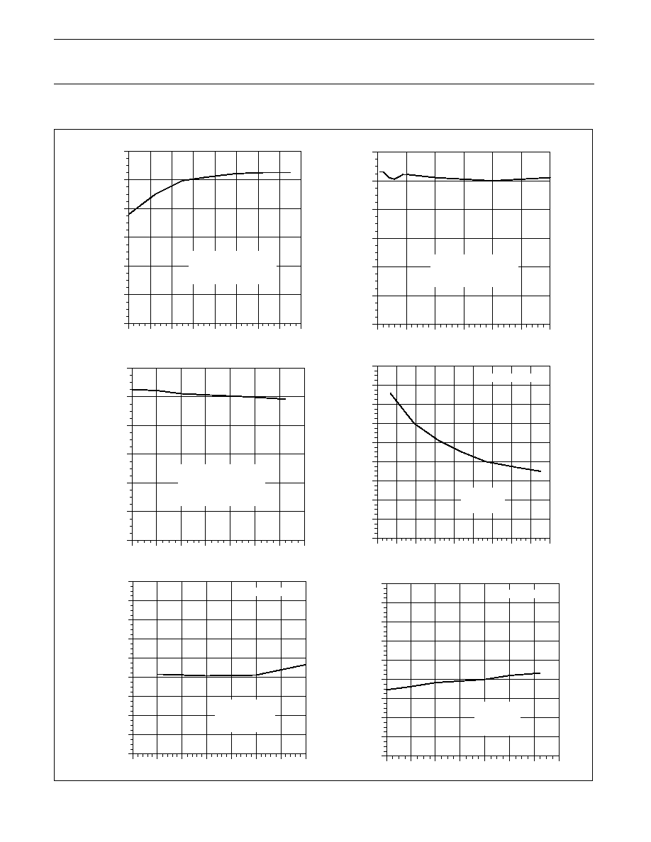
LNA OVERLOAD/NOISE/DISTORTION CHARACTERISTICS
4.5V
V
CC
= V
CCMX
5.5V, Test Fig. 1, unless otherwise specified.
800
FREQUENCY (MHz)
LNA Input 1dB Gain Compression Point vs Frequency
0
P≠1 (dBm)
900
1000
1100
1200
≠5
≠10
≠15
≠20
≠25
≠30
≠40
TEMPERATURE (
∞
C)
LNA Input 1dB Gain Compression Point vs Temperature
0
P≠1 (dBm)
≠5
≠10
≠15
≠20
≠25
≠30
≠20
0
20
40
60
80
100
800
FREQUENCY (MHz)
LNA 50
Noise Figure vs Frequency
3
NF (dB)
900
1000
1100
1200
2.5
2
1.5
1
0.5
0
LNA 50
Noise Figure vs Temperature
3
NF (dB)
2.5
2
1.5
1
0.5
0
≠40
TEMPERATURE (
∞
C)
≠20
0
20
40
60
80
100
F = 900MHz
800
FREQUENCY (MHz)
LNA Input Third-Order Intercept vs Frequency
0
IP3 (dBm)
900
1000
1100
1200
≠2
≠4
≠6
≠8
≠10
≠12
≠14
≠16
≠18
≠20
F2 = F1 + 100kHz
LNA Input Third-Order Intercept vs Temperature
0
IP3 (dBm)
≠2
≠4
≠6
≠8
≠10
≠12
≠14
≠16
≠18
≠20
F1 = 900MHz
≠40
TEMPERATURE (
∞
C)
≠20
0
20
40
60
80
100
F2 = 900.1MHz
TEST FIGURE 2
TEST FIGURE 2
SR00087
Figure 6. LNA Overload/Noise/Distortion Performance Characteristics
Philips Semiconductors
Product specification
NE/SA600
1GHz LNA and mixer
1993 Dec 15
54
MIXER GAIN/NOISE CHARACTERISTICS
4.5V
V
CC
= V
CCMX
5.5V, Test Figure 1, unless otherwise specified.
Mixer Voltage Conversion Gain vs LO Power
12
VOL
T
AGE CONVERSION GAIN (dB)
Frf = 900MHz
≠10
LO POWER (dBm)
10
8
6
4
2
0
≠8
≠6
≠4
≠2
0
2
4
6
Flo = 1GHz
Fif = 100MHz
Scaled to RL1 = RL2 = 1k
Mixer Voltage Conversion Gain vs IF Frequency
12
VOL
T
AGE CONVERSION GAIN (dB)
Frf = 900MHz
0
IF FREQUENCY (MHz)
10
8
6
4
2
0
Flo > Frf
Plo = 0dBm
50
100
150
200
250
300
Mixer Voltage Conversion Gain vs Temperature
12
VOL
T
AGE CONVERSION GAIN (dB)
Frf = 900MHz
≠40
Flo = 1GHz
Fif = 100MHz
Plo = 0dBm
10
8
6
4
2
0
≠20
0
20
40
60
80
100
TEMPERATURE (
∞
C)
Mixer 50
Noise Figure vs LO Power
24
NOISE FIGURE (dB)
≠12
Frf = 881MHz
Plo = 981MHz
LO POWER (dBm)
Fif = 100MHz
22
20
18
16
14
12
10
8
6
≠10
≠8
≠6
≠4
≠2
0
2
4
6
24
Frf = 881MHz
50
IF FREQUENCY (MHz)
Flo > Frf
Plo = 0dBm
IF Tuned to 81MHz
Mixer Noise Figure vs IF Frequency
22
20
18
16
14
12
10
8
6
60
70
80
90
100
110
120
NOISE FIGURE (dB)
Mixer Noise Figure vs Temperature
Frf = 881MHz
≠40
Flo = 981MHz
Fif = 100MHz
Plo = 0dBm
≠20
0
20
40
60
80
100
TEMPERATURE (
∞
C)
24
NOISE FIGURE (dB)
22
20
18
16
14
12
10
8
6
TEST FIGURE 3
TEST FIGURE 3
TEST FIGURE 3
Scaled to RL1 = RL2 = 1k
Scaled to RL1 = RL2 = 1k
SR00088
Figure 7. Mixer Gain/Noise Performance Characteristics

Philips Semiconductors
Product specification
NE/SA600
1GHz LNA and mixer
1993 Dec 15
55
MIXER OVERLOAD/DISTORTION CHARACTERISTICS
4.5
V
CC
= V
CCMX
5.5V, Test Fig. 1, unless otherwise specified
0
Frf = 900MHz
Plo = 1GHz
LO POWER (dBm)
Fif = 100MHz
≠10
≠8
≠6
≠4
≠2
0
2
4
6
≠1
≠2
≠3
≠4
≠5
≠6
≠7
≠8
≠9
≠10
P≠1 (dBm)
Mixer Input 1dB Gain Compression Point vs LO Power
0
≠1
≠2
≠3
≠4
≠5
≠6
≠7
≠8
≠9
≠10
P≠1 (dBm)
Mixer Input 1dB Gain Compression Point vs Temperature
Frf = 900MHz
≠40
Flo = 1GHz
Fif = 100MHz
Plo = 0dBm
≠20
0
20
40
60
80
100
TEMPERATURE (
∞
C)
10
IP3 (dBm)
Mixer Input Third-Order Intercept Point vs LO Power
Frf1 = 900MHz
≠10
Frf2 = 901MHz
Flo = 1GHz
Fif = 100MHz
LO POWER (dBm)
9
8
7
6
5
4
3
2
1
0
≠8
≠6
≠4
≠2
0
2
4
6
10
IP3 (dBm)
Mixer Input Third-Order Intercept Point vs IF Frequency
9
8
7
6
5
4
3
2
1
0
50
75
100
125
150
175
200
Frf1 = 900MHz
Frf2 = 901MHz
Flo > Frf
IF FREQUENCY (MHz)
10
IP3 (dBm)
Mixer Input Third-Order Intercept Point vs RF Frequency
800
Frf1 = X00MHz
Frf2 = X01MHz
Flo > Frf
FREQUENCY (MHz)
9
8
7
6
5
4
3
2
1
0
X = 8, 9, 10, 11, 12
Fif = 100MHz
900
1000
1100
1200
10
IP3 (dBm)
Mixer Input Third-Order Intercept Point vs Temperature
Frf1 = 900MHz
Frf2 = 901MHz
Plo = 0dBm
9
8
7
6
5
4
3
2
1
0
Flo = 1GHz
Fif = 100MHz
≠40
≠20
0
20
40
60
80
100
TEMPERATURE (
∞
C)
TEST FIGURE 2
TEST FIGURE 2
SR00089
Figure 8. Mixer Overload/Distortion Characteristics

Philips Semiconductors
Product specification
NE/SA600
1GHz LNA and mixer
1993 Dec 15
56
MIXER S11/ISOLATION/INTERFERENCE CHARACTERISTICS
4.5
V
CC
= V
CCMX
5.5V, Test Fig. 1, unless otherwise specified
0
S1
1 MAGNITUDE (dB)
Mixer S11 at RF Port
vs Frequency and Temperature
800
FREQUENCY (MHz)
≠5
≠10
≠15
≠20
≠25
≠30
≠35
≠40
900
1000
1100
1200
≠40
∞
C
25
∞
C
85
∞
C
≠40
∞
C
25
∞
C
85
∞
C
800
900
1000
1100
1200
FREQUENCY (MHz)
0
S1
1 MAGNITUDE (dB)
≠5
≠10
≠15
≠20
≠25
Mixer S11 at LO Port
vs Frequency and Temperature
0
OUTPUT
INTERF
. SIGNAL
REL. T
O
OUTPUT
SIGNAL
(dB)
Mixer Output Interferring Signal vs
Input Interferring Signal Strength
Frf = 900MHz
Frf≠interf = 901MHz
Plo = 0dBm
Flo = 1GHz
Fif = 100MHz
INPUT INTERFERRING SIGNAL (dBm)
≠10
≠20
≠30
≠40
≠50
≠60
≠70
≠30
≠25
≠20
≠15
≠10
≠5
0
5
10
Fif≠interf = 98MHz
0
CHANGE IN CONVERSION GAIN
≠5
≠10
≠15
≠20
≠25
≠30
≠35
≠20
≠15
≠10
≠5
0
5
10
15
20
Frf = 900MHz
Plo = 0dBm
Flo = 1GHz
Fif = 100MHz
Conversion Gain Variation vs
RF Signal Overdrive
RF SIGNAL POWER
SR00090
Figure 9. Mixer S11/Isolation/Interference Characteristics
Philips Semiconductors
Product specification
NE/SA600
1GHz LNA and mixer
1993 Dec 15
57
OVERALL PERFORMANCE: ISOLATION CHARACTERISTICS
4.5
V
CC
= V
CCMX
5.5V, Test Fig. 1, unless otherwise specified
Isolation From LNA Output to Mixer
RF Input vs Frequency
0
800
FREQUENCY (MHz)
ISOLA
TION MAGNITUDE (dB)
ENABLE=HI
ENABLE=LO
≠10
≠20
≠30
≠40
≠50
≠60
900
1000
1100
1200
Isolation From LO vs Frequency
0
800
FREQUENCY (MHz)
ISOLA
TION MAGNITUDE (dB)
At LNA input ≠ ENABLE = LO
≠10
≠20
≠30
≠40
≠50
≠60
900
1000
1100
1200
At LNA input ≠ ENABLE = HI
At Mixer RF input
SR00091
Figure 10. Overall Performance: Isolation Characteristics
SPECIFICATIONS
The goal of the Specifications section of the datasheet is to provide
information on the NE/SA600 in such a way that the designer can
estimate statistical variations, and can reproduce the
measurements. To this end the high frequency measurements are
specified with a particular PC board layout. Variations in board
layout will cause parameter variations (sensitive parameters are
discussed in the sections on the LNA and mixer below). For many
RF parameters the
±
3 sigma limits are specified. Statistically only
0.26% of the units will be outside these limits.
The LNA + mixer conversion gain is measured with an incident
900MHz signal and a 83MHZ SAW filter at the IF output. This
measurement along with a gain measurement of the LNA ensure the
correct operation of the chip and also allows a calculation of mixer
conversion gain.
PIN DESCRIPTIONS AND OPERATIONAL LIMITS
RF
INA
Input of LNA, AC coupling required, DC = 0.78V, frequency range
from DC to 2GHz, gain at low frequencies is 40dB -- so be careful
of overload, impedance below 50
, shunt 15-18nH inductor helps
input match and noise figure.
RF
OUTA
Output of LNA, AC coupling required, DC = 1.27V, frequency range
from DC to 2GHz, impedance above 50
.
BYPASS
Bypass capacitor should be 100 times larger than the largest signal
coupling capacitor for the LNA, DC = 1.05V.
RF
INMX
Mixer RF port, AC coupling required, DC = 1.43V, frequency range
from 100MHz to 2.5GHz, impedance close to 50
resistive.
LO
IN
Mixer LO port, AC coupling required, DC=3.35V, frequency range
from 100MHz to 2.5GHz, impedance close to 50
resistive.
IF
OUT
Mixer IF port, open-collector output with 1.6mA DC, frequency range
DC to 1GHz, impedance approximately 1pF capacitive.
Enable
TTL/CMOS compatible input. Bias current approximately zero.
CONVERSION GAIN DEFINITIONS
Referring to the figure above, we define the ratio of V
A
(at the IF
frequency) to V
I
(at the RF frequency) to be the Available Voltage
Conversion Gain, or more simply Voltage Conversion Gain,
VO
10
µ
H
RL1
1k
IF FILTER
LO
RF
VI
VA
RL2
SR00092
Figure 11.
VG
C
+
20 log
V
A
V
I
where V
A
and V
I
are expressed in similar voltage units (such as
peak-to-peak). The voltage output V
A
is decreased by the IF Filter

Philips Semiconductors
Product specification
NE/SA600
1GHz LNA and mixer
1993 Dec 15
58
loss (and any other matching required). Typically, VG
C
is 10.4dB for
the NE/SA600 mixer with the net IF impedance equal to 500
.
It is more common to express the conversion gain in terms of power,
so we have the Power Conversion Gain,
PG
C
+
10 log
P
A
P
I
*
3dB
where P
A
= V
A
2
/ R
IF
and P
I
= V
I
2
/ R
RF
. R
IF
is the net resistance at
the IF frequency at the IF port, and R
RF
is the input impedance at
the mixer RF port. With a 500
IF impedance and a 50
RF input
impedance, the conversion gain works out to ≠2.6dB typically. The
power delivered to the load is down 3dB with respect to the available
power because of loss in R
L1
.
THEORY OF OPERATION
The NE/SA600 is fabricated on the Philips Semiconductors
advanced QUBiC technology that features 1
µ
m channel length
MOSFETs and 13GHz FT bipolar transistors.
LNA
The Low Noise Amplifier (LNA) is a two stage design incorporating
feedback to stablize the amplifier. An external bypass capacitor of
(typically) 0.01
µ
F is used. The inputs and outputs are matched to
50
. The amplifier has two gain states: when the ENABLE pin is
taken high, the amplifier draws 9mA of current and has 16dB of gain
at 900MHz. When the ENABLE pin is low, the amplifier current goes
to zero, and the amplifier is replaced by a thru. Typical loss for the
thru is 7dB. This dual-gain state approach can be used in
bang-bang control systems to achieve a low gain, high overload
front-end as well as the more usual high gain, low overload
front-end.
The amplifier has gain to frequencies past 2GHz, but a practical
upper end is 1.6-1.7GHz. Both the input match and the noise figure
(NF) can be improved with a shunt 15-18nH inductor at the input.
Typically, the gain increases 0.4dB, the match improves to 13-16dB,
and the noise figure drops to 1.95-2dB. Variations of any of the RF
parameters with V
CC
is negliglible, and variation with temperature is
minimal.
Mixer
The mixer is a single-balanced topology designed to draw very low
current, typically 4mA, and provide a very high input third-order
intermodulation intercept point , typically IP3=+6dBm. The RF and
LO ports impedances are nearly 50
resistive, and the IF output is
an open collector. The open-collector output allows direct
interfacing with high impedance IF filters, such as surface acoustic
wave (SAW) filters without the need for external step-up
transformers (which are needed for 50
output mixers).
The basic mixer is functional from DC to well over 2.5GHz, but RF
and LO return losses degrade below 100MHz. The IF output can be
used from DC to 500MHz or more, although typically the
intermediate frequency is in the range 45-120MHz in many 900MHz
receivers. To achieve the lowest noise, the LO drive level should be
increased as high as possible, consistent with power dissipation
limitations.
POWER SUPPLY ISSUES
V
CC
bypassing is important, but not extremely critical because of
the internal supply regulation of the NE/SA600. The Pin 1 V
CC
supplies the LNA and powers overhead circuitry. Typical current
draw is 9.8mA while enable is high (1mA powered down). The Pin
14 V
CCMX
powers the mixer and typically has 3.2mA of current
(assuming an inductor biasing the IFout back to V
CCMX
). Care must
be taken to avoid bringing any IC pin above V
CC
by more than 0.3V,
or below any ground by more than 0.3V. For example, this can
occur if the enable pin is fed from a microcontroller that is powered
up quicker than the NE/SA600. In this condition the internal
electrostatic discharge (ESD) protection network may turn-on,
possibly causing a part misfunction. Generally this condition is
reversible, so long as the source creating the overstress is current
limited to less than 100mA. To avoid the problem, make sure both
V
CC
pins are tied together near the IC, and install a 1k
resistor in
series with the enable pin if it is likely to go above V
CC
.
BOARD LAYOUT CONSIDERATIONS
The LNA is sensitive to mutual inductance from the input to ground.
Therefore long narrow input traces will degrade the input match.
Ideally, a top side ground-plane should be employed to maximize
LNA gain and minimize stray coupling (such as LO to antenna). To
avoid amplifier peaking, the output and input grounds should not be
run together. Attach both grounds to a solid ground plane. A solid
ground plane beneath the package will maximize gain. Top side to
back side ground through holes are highly recommended.
The mixer is relatively insensitive to grounding. Care should be
taken to minimize the capacitance on the RF port (Pin 11) for best
noise figure. Also, the capacitance on the IFout pin must be kept
small to avoid conversion gain rolloff when using high IF
frequencies. The purpose of the inductor from IFout to V
CC
is to set
the midpoint of the IF swing to be V
CC
. Without this inductor the
part is sensitive to output overload under low V
CC
(V
CC
= 4.5V) and
hot temperature conditions. The V
CCMX
pin must be kept at the
same potential as the V
CC
pin.
APPLICATIONS INFORMATION
The NE/SA600 is a high performance, wide-band, low power, low
noise amplifier (LNA) and mixer circuit integrated in a BiCMOS
technology. It is ideally suited for RF receiver front-ends for both
analog and digital communications systems.
There are several advantages to using the NE/SA600 as a high
frequency front-end block instead of a discrete implementation. First
is the simplicity of use. The NE/SA600 does not need any external
biasing components. Due to the higher level of integration and
small footprint (SO14) package it occupies less space on the printed
circuit board and reduces the manufacturing cost of the system.
Also the higher level of integration improves the reliability of the LNA
and mixer over a discrete implementation with several components.
The LNA thru mode in NE/SA600 helps reduce power consumption
in applications where the amplifiers can be disabled due to higher
received signal strength (RSSI). Other advantages of this feature
are described later in this section.
The mixer is an active mixer with excellent conversion gain at low
LO input levels, so LO levels as low as -5dBm to -10dBm can be
used depending on the applications requirement for mixer gain,
mixer noise figure and mixer third order intercept point. This
reduces the LO drive requirements from the VCO buffer, thus
reducing its current consumption. Also, due to lower LO levels, the
shielding requirements can be minimized or eliminated, resulting in
substantial cost savings and weight and space reduction.

Philips Semiconductors
Product specification
NE/SA600
1GHz LNA and mixer
1993 Dec 15
59
And last but not least, is the impedance matching at LNA inputs and
outputs and mixer RF and LO input ports. Only those who have
toiled through discrete transistor implementations for 50
input and
output impedance matching can truly appreciate the elegance and
simplicity of the NE/SA600 input and output impedance matching to
50
. Also, the mixer output impedance is high, so matching to a
crystal or SAW IF filter becomes extremely easy without the need for
additional IF impedance transformers (tapped-C networks with
inductors or baluns).
The NE/SA600 applications and demo board features standard low
cost 62mil FR-4 board. A top-side ground plane is used and 50
coplanar transmission lines are used. LO and RF
INA
traces are
perpendicular. Provisions for the image reject filter between RF
OUTA
and RF
INMX
are provided. A simple LC match for 80MHz IF is used
so that 50
measurements can be made on the demo board.
The NE/SA600 applications evaluation board schematic is shown in
Figure 1. The V
CC
(Pin 1) and V
CCMX
(Pin 14) are tied together and
the power supply is bypassed with capacitors C5 and C6. These
capacitors should be placed as close to the device as practically
possible.
C1 is the DC blocking capacitor to the input of the LNA. L1 provides
additional input matching to the LNA for an improved return loss
(S11). This inductor can be a surface-mount component or can be
easily drawn on the printed circuit board (small spiral or serpentine).
This additional match improves the gain of the LNA by 0.4dB and
lowers the noise figure to 2dB or less. If the typical gain of the LNA
of 16dB is acceptable with 2.2dB of noise figure, then L1 can be
eliminated. If the LNA input is fed from a duplexer or selectivity
filter after the antenna, C1 can also be eliminated since the filter will
also provide DC blocking. The LNA bypass capacitor C3 should be
at least 100 times C1 or C9 for low frequency stability. Switch S1
toggles the LNA gain/through function. R1 is used only to limit the
maximum current into the enable pin and only necessary if enable
may power up before the V
CC
.
C4 is a DC blocking capacitor for the LO input pin and may not be
needed in actual applications if the VCO output is isolated and will
not upset the internal DC biasing of the mixer. The image reject
filter goes between the output of the LNA and the RF input to the
mixer. Since the LO input, RF output and mixer input are all 50
matched impedances internally, there is no need for any external
components. C8 and C9 are DC blocking capacitors to the
connectors and will not be needed in an actual application.
R2 and L2 are the load to the mixer output which is typical of the IF
crystal or SAW filters. C2 and L3 provide a match from the high
impedance mixer output to a 50
test set-up (spectrum analyzer,
etc.) and C7 is a DC blocking capacitor for the mixer output.
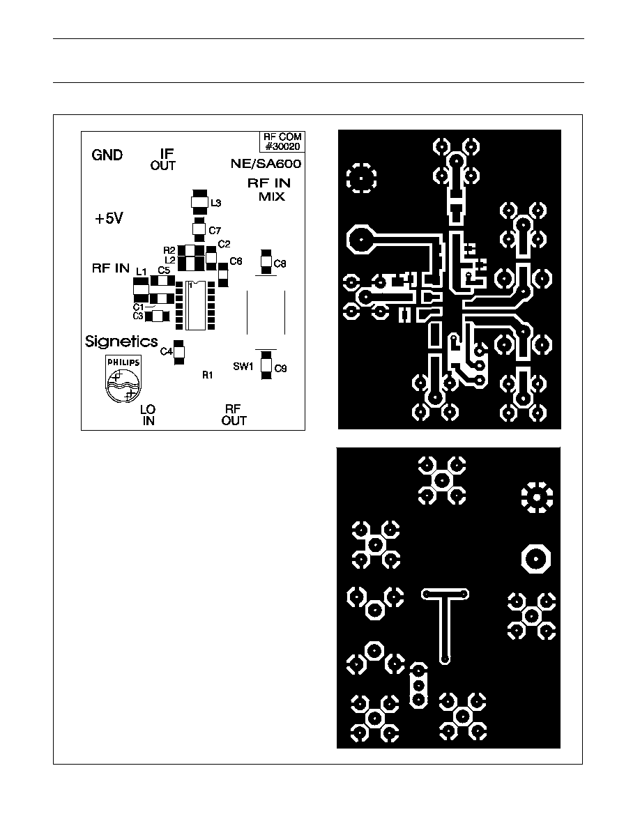
The printed circuit board layout for the schematic of Figure 1 is
shown in Figure 14. It is a very simple printed circuit board layout
with all the components on a single side. The layout also
accomodates a two pole image reject filter between the LNA outupt
and mixer input. All the input and output traces to the LNA and
mixer should be 50
tracks with the exception of mixer output,
which can be very narrow due to the higher impedances of the filter.
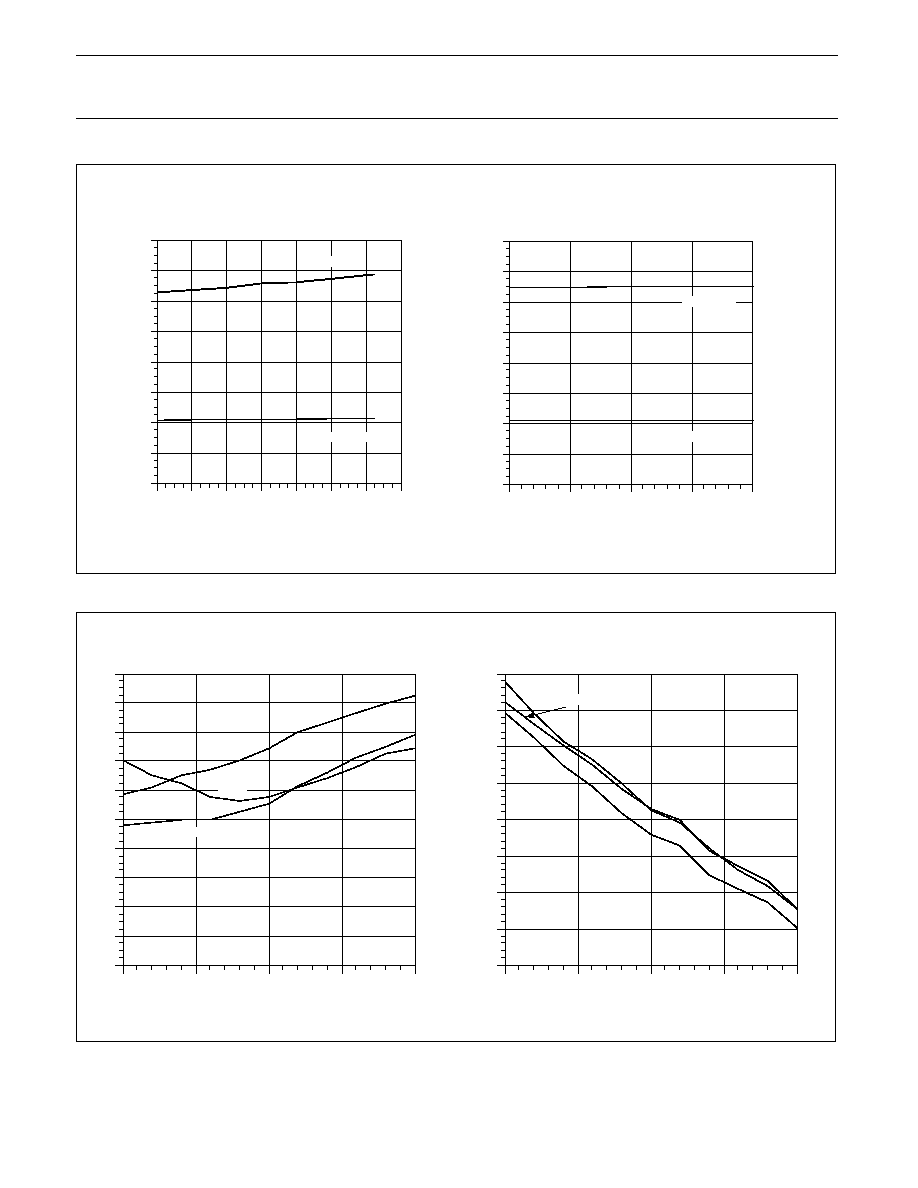
The NE/SA600 internal supply is very well regulated. This is seen
from Figure 15 which shows the I
CC
vs. V
CC
for the NE/SA600.
Table NO TAG shows the S11, S21, S22 and S21 for the LNA from
800-1200MHz. Typical measurements at 900MHz for the critical
parameters such as gain, noise figure, IP
3
, 1dB compression point,
etc. as measured on an applications evaluation board are as follows
:
LNA gain = 16.5dB
LNA through = ≠7dB
Mixer gain =≠3dB (into a 50
load)
LNA noise figure = 2dB
Mixer noise figure = 14dB
LNA IP
3
= ≠10dBm (in gain mode)
LNA IP
3
= +26dBm (in through mode)
LNA 1dB compression point = ≠20dBm
Mixer 1dB compression point = ≠4dBm
The shunt inductor L1 for input match is optional. Figure 16 shows
the effect of the inductor value from 8.2nH to 15nH on gain, noise
figure and input match.
The total power gain for the LNA and mixer (excluding the image
reject filter) in a system where the output of the mixer is loaded with
50
is about 14dB. In an actual system the output impedance of
the mixer is usually much higher than 50
(more like 1k
or higher)
and so it is more important to consider the voltage gain from the
input at the LNA to the mixer output. The voltage gain in this case
will be about 29.85V/V. The total noise figure for the LNA and mixer
combination is be about 3.27dB. The input third order intercept
point for the LNA and mixer is about -11dBm. In the LNA through
mode, the intercept point for the combination is higher than
+19dBm. This LNA through feature provides an additional boost to
the total dynamic range of the system.
The NE/SA600 finds applications in many areas of RF
communications. It is an ideal down converter block for high
performance, low cost, low power RF communications transceivers.
The front-end of a typical AMPS/TACS/NMT/TDMA/CDMA cellular
phone is shown in Figure 13. This could also be the front-end of a
VHF/UHF handheld transceiver, UHF cordless telephone or a
spread spectrum system.
The antenna is connected to the duplexer input. The receiver output
of the duplexer is connected to the RF input of the LNA. If the
additional improvement in noise figure and gain are not needed to
meet the system specifications then L1 and C1 can be eliminated.
In TDMA systems, the NE/SA600 can be totally powered down by
Q1 and the two resistors. In this mode the current consumption will
be zero mA. Care should be taken in the software of the system to
insure that the enable pin on NE/SA600 tied to the LNA gain control
port is held low while the device is in total power down mode. L2
and C2 can be tuned to the IF frequency and to match to the IF filter
impedance.
A complete analysis of the front-end shows that the total voltage
gain from the antenna input to the mixer output is about 9.5V/V. This
value includes a 3.2dB loss for the duplexer and a 1.8dB loss for the
bandpass filter. The noise figure as referred to the antenna is 7dB
and the input third order intercept point is about -7.5dBm. In LNA
through mode the input third order intercept point increases to about
+24dBm.
During normal operation of a handheld RF receiver the received
signal strength (RSSI) is nominally greater than -100dBm. The
signal only drops below this level due to severe multipath fading,
shadow effect or when the receiver is at extreme fringes of cell
coverage. The LNA through mode can be used here as a two step
gain control such that when RSSI is below a certain threshold level
(e.g. -90dBm), the LNA has a -7dB loss and the total current
consumption of the NE/SA600 is only 4.3mA. The sensitivity of the
system will not suffer because the received RF signal is much higher
than the noise floor of the system. When the RSSI falls below a
certain threshold (e.g. -95dBm) the LNA is enabled to give the full

Philips Semiconductors
Product specification
NE/SA600
1GHz LNA and mixer
1993 Dec 15
60
16.5dB of gain with 2dB of noise figure. In this mode the current
consumption is increased to 13mA. But for hand-held equipment,
the average current consumption will be closer to 5-6mA. The other
advantage of the LNA through mode besides power savings is the
input overload characteristics. Due to the much higher input third
order intercept point of the LNA (+26dBm), the receiver is immune to
strong adjacent channel interference. Implementing this feature with
an FM/IF device such as the NE625/7 with fast RSSI response and
a window comparator toggling the LNA mode of NE/SA600, a fast
two-step AGC with response time less than 10
µ
s can be achieved.
This is a very useful feature to equalize multipath fading effects in a
mobile radio system.
In conclusion, the NE/SA600 offers higher level of integration, higher
reliability, higher level of performance, ease of use, simpler system
design at a cost lower than the discrete multi-transistor
implementations. In addition, the NE/SA600 provides unique
features to enhance receiver performance which are almost
unattainable with discrete implementations.
14
13
12
11
4
3
2
1
NE/SA600
10
9
8
7
6
5
BANDPASS
FILTER
LO INPUT
BYPASS
RF
INPUT
900MHz
10nF
100pF
0.1
µ
F
MIXER IN
RF OUT
IF OUT
470nH
100pF
100pF
100pF
C6
10nF
C2
4.7pF
C7
10nF
10
µ
H
L3
R2
1k
L2
C8
C9
IN
OUT
VC
C
GNDB
RF INA
GNDA1
VCCMX
GNDMX
IFOUT
RF INMX
BYPASS
GNDLO
LOIN
GNDA2
ENABLE
RF OUTA
R1
1k
S1
C5
15nH
L1
C3
C4
VCC
VCC
C1
SR00093
Figure 12.

Philips Semiconductors
Product specification
NE/SA600
1GHz LNA and mixer
1993 Dec 15
61
14
13
12
11
4
3
2
1
NE/SA600
10
9
8
7
6
5
BANDPASS
FILTER
10nF
100pF
0.1
µ
F
C5
10nF
C2
L2
IN
OUT
VC
C
GNDB
RF INA
GNDA1
VCCMX
GNDMX
IFOUT
RF INMX
BYPASS
GNDLO
LOIN
GNDA2
ENABLE
RF OUTA
R1
1k
C4
15nH
L1
C3
LNA GAIN CONTROL
VCC
I
O
G
1
2
3
To FM-IF Circuits
NE605/6/7/8
IF FILTER
POWER DOWN
DUPLEXER
C1
from VCO/Synthesizer UMA1014
Q1
BCX17
5.1k
15k
3
1
2
from Power Amp
ANTENNA
SR00094
Figure 13.
Philips Semiconductors
Product specification
NE/SA600
1GHz LNA and mixer
1993 Dec 15
62
TOP
BOTTOM
SILKSCREEN
SR00095
Figure 14. PC Board Layout
Philips Semiconductors
Product specification
NE/SA600
1GHz LNA and mixer
1993 Dec 15
63
Total Supply Current vs Temperature
16
≠40
TEMPERATURE (
∞
C)
I (mA)
ENABLE=HI
ENABLE=LO
14
12
10
8
6
4
2
0
CC
≠20
0
20
40
60
80
100
Total Supply Current vs V
CC
16
4.5
VCC (V)
I (mA)
ENABLE=HI
ENABLE=LO
14
12
10
8
6
4
2
0
CC
4.75
5
5.25
5.5
SR00096
Figure 15.
FREQUENCY (MHz)
700
800
900
1000
1100
NF (dB)
3
2.8
2.6
2.4
2.2
2
1.8
1.6
1.4
1.2
1
LNA Noise Figure vs. Frequency
and Shunt Inductance
700
800
900
1000
1100
S21 MAGNITUDE (dB)
20
19
18
17
16
15
14
13
12
FREQUENCY (MHz)
LNA Gain vs. Frequency
and Shunt Inductance
0nH
8.2nH
15nH
0nH
8.2nH
15nH
SR00097
Figure 16.