 | –≠–ª–µ–∫—Ç—Ä–æ–Ω–Ω—ã–π –∫–æ–º–ø–æ–Ω–µ–Ω—Ç: PCA9532 | –°–∫–∞—á–∞—Ç—å:  PDF PDF  ZIP ZIP |

Philips
Semiconductors
PCA9532
16-bit I
2
C LED dimmer
Product data
Supersedes data of 2003 Feb 26
2003 May 02
INTEGRATED CIRCUITS

Philips Semiconductors
Product data
PCA9532
16-bit I
2
C LED dimmer
2
2003 May 02
FEATURES
∑
16 LED drivers (on, off, flashing at a programmable rate)
∑
2 selectable, fully programmable blink rates (frequency and duty
cycle) between 0.625 and 160 Hz (6.4 seconds and
6.25 milliseconds)
∑
256 brightness steps
∑
Input/outputs not used as LED drivers can be used as regular
GPIOs
∑
Internal oscillator requires no external components
∑
I
2
C-bus interface logic compatible with SMBus
∑
Internal power-on reset
∑
Noise filter on SCL/SDA inputs
∑
Active-LOW reset input
∑
16 open drain outputs directly drive LEDs to 25 mA
∑
Controlled edge rates to minimize ground bounce
∑
No glitch on power-up
∑
Supports hot insertion
∑
Low stand-by current
∑
Operating power supply voltage range of 2.3 V to 5.5 V
∑
0 to 400 kHz clock frequency
∑
ESD protection exceeds 2000 V HBM per JESD22-A114,
150 V MM per JESD22-A115 and 1000 V CDM per JESD22-C101
∑
Latch-up testing is done to JEDEC Standard JESD78 which
exceeds 100 mA
∑
Packages offered: SO24, TSSOP24, HVQFN24
DESCRIPTION
The PCA9532 is a 16-bit I
2
C-bus and SMBus I/O expander
optimized for dimming LEDs in 256 discrete steps for
Red/Green/Blue (RGB) color mixing and back light applications.
The PCA9532 contains an internal oscillator with two user
programmable blink rates and duty cycles coupled to the output
PWM. The LED brightness is controlled by setting the blink rate high
enough (> 100 Hz) that the blinking cannot be seen and then using
the duty cycle to vary the amount of time the LED is on and thus the
average current through the LED.
The initial set-up sequence programs the two blink rates/duty cycles
for each individual PWM. From then on, only one command from the
bus master is required to turn individual LEDs ON, OFF, BLINK
RATE 1 or BLINK RATE 2. Based on the programmed frequency
and duty cycle, BLINK RATE 1 and BLINK RATE 2 will cause the
LEDs to appear at a different brightness or blink at periods up to
1.6 seconds. The open drain outputs directly drive the LEDs with
maximum output sink current of 25 mA per bit and 200 mA per
package (100 mA per octal).
To blink LEDs at periods greater than 1.6 seconds the bus master
(MCU, MPU, DSP, chipset, etc.) must send repeated commands to
turn the LED on and off as is currently done when using normal I/O
Expanders like the Philips PCF8575 or PCA9555. Any bits not used
for controlling the LEDs can be used for General Purpose Parallel
Input/Output (GPIO) expansion which provides a simple solution
when additional I/O is needed for ACPI power switches, sensors,
pushbuttons, alarm monitoring, fans, etc.
The active-LOW hardware reset pin (RESET) and Power-On Reset
(POR) initializes the registers to their default state, all zeroes,
causing the bits to be set HIGH (LED off).
Three hardware address pins on the PCA9532 allow eight devices
to operate on the same bus.
ORDERING INFORMATION
PACKAGES
TEMPERATURE RANGE
ORDER CODE
TOPSIDE MARK
DRAWING NUMBER
24-pin plastic SO
-40 to +85
∞
C
PCA9532D
PCA9532D
SOT137-1
24-pin plastic TSSOP
-40 to +85
∞
C
PCA9532PW
PCA9532
SOT355-1
24-pin plastic HVQFN
-40 to +85
∞
C
PCA9532BS
9532
SOT616-1
Standard packing quantities and other packaging data is available at www.philipslogic.com/packaging.
I
2
C is a trademark of Philips Semiconductors Corporation.

Philips Semiconductors
Product data
PCA9532
16-bit I
2
C LED dimmer
2003 May 02
3
PIN CONFIGURATION -- SO, TSSOP
1
2
3
4
5
6
7
8
9
10
11
12
13
14
15
16
17
18
19
20
21
22
23
24
A0
A1
A2
LED0
LED1
LED2
LED3
LED4
LED5
LED6
LED7
V
DD
SDA
SCL
RESET
LED15
LED14
LED13
LED11
LED12
LED10
LED9
LED8
V
SS
SW00931
Figure 1. Pin configuration -- SO, TSSOP
PIN CONFIGURATION -- HVQFN
18
17
16
15
14
7
8
9
10
11
1
2
3
4
5
24
23
22
21
20
su01668
TOP VIEW
LED0
RESET
6
13
12
19
LED1
LED2
LED3
LED4
LED5
LED11
LED12
LED13
LED14
LED15
LED6
LED7
LED8
LED9
LED10
A2
A1
A0
V
SDA
SCL
DD
V
SS
Figure 2. Pin configuration -- HVQFN
PIN DESCRIPTION
SO, TSSOP
PIN
NUMBER
HVQFN
PIN
NUMBER
SYMBOL
FUNCTION
1
22
A0
Address input 0
2
23
A1
Address input 1
3
24
A2
Address input 2
4, 5, 6, 7, 8, 9,
10, 11
1, 2, 3, 4, 5, 6,
7, 8
LED0-7
LED driver 0-7
12
9
V
SS
Supply ground
13, 14, 15, 16,
17, 18, 19, 20
10, 11, 12, 13,
14, 15, 16, 17
LED8-15
LED driver 8-15
21
18
RESET
Active-LOW reset input
22
19
SCL
Serial clock line
23
20
SDA
Serial data line
24
21
V
DD
Supply voltage

Philips Semiconductors
Product data
PCA9532
16-bit I
2
C LED dimmer
2003 May 02
4
BLOCK DIAGRAM
PWM0
REGISTER
PWM1
REGISTER
PRESCALER 0
REGISTER
PRESCALER 1
REGISTER
I
2
C-BUS
CONTROL
LEDx
A2
A1
A0
INPUT
FILTERS
SCL
SDA
OSCILLATOR
POWER-ON
RESET
V
DD
V
SS
SW02045
1
0
BLINK0
BLINK1
RESET
NOTE: ONLY ONE I/O SHOWN FOR CLARITY
LED SELECT (LSx)
REGISTER
INPUT
REGISTER
PCA9532
Figure 3. Block diagram

Philips Semiconductors
Product data
PCA9532
16-bit I
2
C LED dimmer
2003 May 02
5
DEVICE ADDRESSING
Following a START condition the bus master must output the
address of the slave it is accessing. The address of the PCA9532 is
shown in Figure 4. To conserve power, no internal pull-up resistors
are incorporated on the hardware selectable address pins and they
must be pulled HIGH or LOW.
1
1
0
0
A2
A1
A0
SLAVE ADDRESS
su01420
FIXED
HARDWARE SELECTABLE
R/W
Figure 4. Slave address
The last bit of the address byte defines the operation to be
performed. When set to logic 1 a read is selected while a logic 0
selects a write operation.
CONTROL REGISTER
Following the successful acknowledgement of the slave address,
the bus master will send a byte to the PCA9532 which will be stored
in the Control Register. This register can be read and written via the
I
2
C-bus.
0
0
AI
B2 B1 B0
0
SW00898
B3
AUTO-INCREMENT FLAG
REGISTER ADDRESS
RESET STATE: 00h
Figure 5. Control register
CONTROL REGISTER DEFINITION
B3
B2
B1
B0
REGISTER
NAME
TYPE
REGISTER
FUNCTION
0
0
0
0
INPUT0
READ
INPUT
REGISTER 0
0
0
0
1
INPUT1
READ
INPUT
REGISTER 1
0
0
1
0
PSC0
READ/
WRITE
FREQUENCY
PRESCALER 0
0
0
1
1
PWM0
READ/
WRITE
PWM
REGISTER 0
0
1
0
0
PSC1
READ/
WRITE
FREQUENCY
PRESCALER 1
0
1
0
1
PWM1
READ/
WRITE
PWM
REGISTER 1
0
1
1
0
LS0
READ/
WRITE
LED 0-3
SELECTOR
0
1
1
1
LS1
READ/
WRITE
LED 4-7
SELECTOR
1
0
0
0
LS2
READ/
WRITE
LED 8-11
SELECTOR
1
0
0
1
LS3
READ/
WRITE
LED 12-15
SELECTOR
REGISTER DESCRIPTION
The lowest 3 bits are used as a pointer to determine which register
will be accessed.
If the auto-increment flag (AI) is set, the four low order bits of the
Control Register are automatically incremented after a read or write.
This allows the user to program the registers sequentially. The
contents of these bits will rollover to `0000' after the last register is
accessed.
When auto-increment flag is set (AI = 1) and a read sequence is
initiated, the sequence must start by reading a register different from
`0' (B3 B2 B1 B0
0
0 0 0 0)
Only the 4 least significant bits are affected by the AI flag.
Unused bits must be programmed with zeroes.
INPUT0 -- INPUT REGISTER 1
bit
I7
I6
I5
I4
I3
I2
I1
I0
default
0
0
0
0
0
0
0
0
The INPUT register 1 reflects the state of the device pins (inputs 0
to 7). Writes to this register will be acknowledged but will have no
effect.
INPUT1 -- INPUT REGISTER 2
bit
I15
I14
I13
I12
I11
I10
I9
I8
default
0
0
0
0
0
0
0
0
The INPUT register 1 reflects the state of the device pins (inputs 8
to 15). Writes to this register will be acknowledged but will have no
effect.
PSC0 -- FREQUENCY PRESCALER 0
bit
7
6
5
4
3
2
1
0
default
0
0
0
0
0
0
0
0
PSC0 is used to program the period of the PWM output.
The period of BLINK0
+
(PSC0
)
1)
152
PWM0 -- PWM REGISTER 0
bit
7
6
5
4
3
2
1
0
default
1
0
0
0
0
0
0
0
The PWM0 register determines the duty cycle of BLINK0. The
outputs are LOW (LED on) when the count is less than the value in
PWM0 and HIGH (LED off) when it is greater. If PWM0 is
programmed with 00h, then the PWM0 output is always HIGH
(LED off).
The duty cycle of BLINK0 is:
PWM0
256
PSC1 -- FREQUENCY PRESCALER 1
bit
7
6
5
4
3
2
1
0
default
0
0
0
0
0
0
0
0
PSC1 is used to program the period of PWM output.
The period of BLINK1
+
(PSC1
)
1)
152
PWM1 -- PWM REGISTER 1
bit
7
6
5
4
3
2
1
0
default
1
0
0
0
0
0
0
0
The PWM1 register determines the duty cycle of BLINK1. The
outputs are LOW (LED on) when the count is less than the value in
PWM1 and HIGH (LED off) when it is greater. If PWM1 is
programmed with 00h, then the PWM1 output is always HIGH
(LED off).
The duty cycle of BLINK1 is:
PWM1
256

Philips Semiconductors
Product data
PCA9532
16-bit I
2
C LED dimmer
2003 May 02
6
LS0 -- LED 0-3 SELECTOR
LED 3
LED 2
LED 1
LED 0
bit
7
6
5
4
3
2
1
0
default
0
0
0
0
0
0
0
0
LS1 -- LED 4-7 SELECTOR
LED 7
LED 6
LED 5
LED 4
bit
7
6
5
4
3
2
1
0
default
0
0
0
0
0
0
0
0
LS2 -- LED 8-11 SELECTOR
LED 11
LED 10
LED 9
LED 8
bit
7
6
5
4
3
2
1
0
default
0
0
0
0
0
0
0
0
LS3 -- LED 12-15 SELECTOR
LED 15
LED 14
LED 13
LED 12
bit
7
6
5
4
3
2
1
0
default
0
0
0
0
0
0
0
0
The LSx LED select registers determine the source of the LED data.
00 = Output is set Hi-Z (LED off - default)
01 = Output is set LOW (LED on)
10 = Output blinks at PWM0 rate
11 = Output blinks at PWM1 rate
Philips Semiconductors
Product data
PCA9532
16-bit I
2
C LED dimmer
2003 May 02
7
POWER-ON RESET
When power is applied to V
DD
, an internal Power-On Reset holds
the PCA9532 in a reset state until V
DD
has reached V
POR
. At this
point, the reset condition is released and the PCA9532 registers are
initialized to their default states, all the outputs in the off state.
EXTERNAL RESET
A reset can be accomplished by holding the RESET pin LOW for a
minimum of t
W
. The PCA9532 registers and I
2
C state machine will
be held in their default state until the RESET input is once again
HIGH.
This input requires a pull-up resistor to V
DD
.
CHARACTERISTICS OF THE I
2
C-BUS
The I
2
C-bus is for 2-way, 2-line communication between different ICs
or modules. The two lines are a serial data line (SDA) and a serial
clock line (SCL). Both lines must be connected to a positive supply
via a pull-up resistor when connected to the output stages of a device.
Data transfer may be initiated only when the bus is not busy.
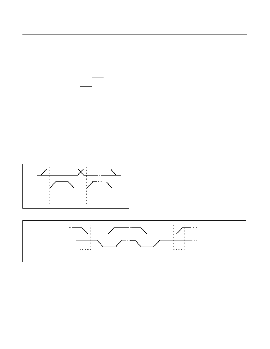
Bit transfer
One data bit is transferred during each clock pulse. The data on the
SDA line must remain stable during the HIGH period of the clock
pulse as changes in the data line at this time will be interpreted as
control signals (see Figure 6).
SDA
SCL
SW00363
data line
stable;
data valid
change
of data
allowed
Figure 6. Bit transfer
Start and stop conditions
Both data and clock lines remain HIGH when the bus is not busy. A
HIGH-to-LOW transition of the data line, while the clock is HIGH is
defined as the start condition (S). A LOW-to-HIGH transition of the
data line while the clock is HIGH is defined as the stop condition (P)
(see Figure 7).
System configuration
A device generating a message is a transmitter: a device receiving
is the receiver. The device that controls the message is the master
and the devices which are controlled by the master are the slaves
(see Figure 8).
SDA
SCL
SW00365
S
P
SDA
SCL
START condition
STOP condition
Figure 7. Definition of start and stop conditions

Philips Semiconductors
Product data
PCA9532
16-bit I
2
C LED dimmer
2003 May 02
8
MASTER
TRANSMITTER/
RECEIVER
SLAVE
RECEIVER
SLAVE
TRANSMITTER/
RECEIVER
MASTER
TRANSMITTER
MASTER
TRANSMITTER/
RECEIVER
SDA
SCL
SW00366
I
2
C
MULTIPLEXER
SLAVE
Figure 8. System configuration
Acknowledge
The number of data bytes transferred between the start and the stop conditions from transmitter to receiver is not limited. Each byte of eight bits
is followed by one acknowledge bit. The acknowledge bit is a HIGH-level put on the bus by the transmitter whereas the master generates an
extra acknowledge related clock pulse.
A slave receiver which is addressed must generate an acknowledge after the reception of each byte. Also a master must generate an
acknowledge after the reception of each byte that has been clocked out of the slave transmitter. The device that acknowledges has to pull down
the SDA line during the acknowledge clock pulse, so that the SDA line is stable LOW during the HIGH period of the acknowledge related clock
pulse, set-up and hold times must be taken into account.
A master receiver must signal an end of data to the transmitter by not generating an acknowledge on the last byte that has been clocked out of
the slave. In this event, the transmitter must leave the data line HIGH to enable the master to generate a stop condition.
DATA OUTPUT
BY TRANSMITTER
SCL FROM
MASTER
SW00368
DATA OUTPUT
BY RECEIVER
1
2
8
9
S
START condition
clock pulse for
acknowledgement
acknowledge
not acknowledge
Figure 9. Acknowledgement on the I
2
C-bus

Philips Semiconductors
Product data
PCA9532
16-bit I
2
C LED dimmer
2003 May 02
9
Bus transactions
A1
A0
1
2
SCL
WRITE TO
REGISTER
DATA OUT
FROM PORT
3
4
5
6
7
8
SDA
S
0
A
A
A
1
1
0
0
A2
DATA 1
slave address
data to register
start condition
R/W
acknowledge
from slave
acknowledge
from slave
acknowledge
from slave
t
pv
DATA 1 VALID
SW02000
9
B0
0
0
0
AI
B3
B2
B1
command byte
Figure 10. WRITE to register
0
0
A2
A1
A0
1
1
0
0
A0
1
1
S
0
A
A
A
acknowledge
from slave
R/W
acknowledge
from slave
A
P
NA
acknowledge
from slave
acknowledge
from master
S
DATA
DATA
R/W
first byte
at this moment master-transmitter
becomes master-receiver and
slave-receiver becomes
slave-transmitter
last byte
SW01099
no acknowledge
from master
1
slave address
data from register
data from register
slave address
auto-increment
register address
if AI = 1
A1
A2
AI B3
B0
0
0
B1
B2
0
Figure 11. READ from register
1
1
0
0
A2
A1
A0
READ FROM
PORT
DATA INTO
PORT
SDA
S
1
A
A
DATA 1
DATA 4
slave address
data from port
data from port
start condition
R/W
acknowledge
from slave
acknowledge
from master
stop
condition
t
ps
DATA 4
DATA 2
P
DATA 3
t
ph
SW01096
no acknowledge
from master
NA
DATA 1
NOTE:
1. This figure assumes the command byte has previously been programmed with 00h.
Figure 12. READ input port register
Philips Semiconductors
Product data
PCA9532
16-bit I
2
C LED dimmer
2003 May 02
10
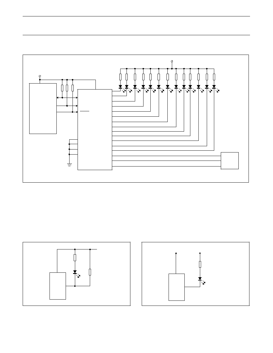
APPLICATION DATA
PCA9532
A1
A0
V
SS
SDA
SCL
RESET
V
DD
I
2
C/SMBus MASTER
SW02044
SDA
SCL
A2
LED0
LED1
LED2
LED3
LED4
LED5
LED6
LED7
5 V
5 V
LED8
LED9
LED10
LED11
LED12
LED13
LED14
LED15
GPIOs
Note: LED0 to LED12 are used as LED drivers
LED13 to LED15 are used as regular GPIOs.
Figure 13. Typical application
Minimizing I
DD
when the I/O is used to control LEDs
When the I/Os are used to control LEDs, they are normally connected to V
DD
through a resistor as shown in Figure 13. Since the LED acts as a
diode, when the LED is off the I/O V
IN
is about 1.2 V less than V
DD
. The supply current, I
DD
, increases as V
IN
becomes lower than V
DD
and is
specified as
I
DD
in the DC characteristics table.
Designs needing to minimize current consumption, such as battery power applications, should consider maintaining the I/O pins greater than or
equal to V
DD
when the LED is off. Figure 14 shows a high value resistor in parallel with the LED. Figure 15 shows V
DD
less than the LED supply
voltage by at least 1.2 V. Both of these methods maintain the I/O V
IN
at or above V
DD
and prevents additional supply current consumption when
the LED is off.
V
DD
V
DD
LEDx
LED
100 k
SW02086
Figure 14. High value resistor in parallel with the LED
V
DD
3.3 V
LEDx
LED
SW02087
5 V
Figure 15. Device supplied by a lower voltage

Philips Semiconductors
Product data
PCA9532
16-bit I
2
C LED dimmer
2003 May 02
11
Programming example
The following example will show how to set LED0 to LED3 on. It will
then set LED4 and LED5 to blink at 1 Hz at a 50% duty cycle. LED6
and LED7 will be set to be dimmed at 25% of their brightness (duty
cycle = 25%). LED8 to LED15 will be set to off.
Table 1.
I
2
C-bus
Start
S
PCA9532 address with A0-A2 = LOW
C0h
PSC0 subaddress + auto-increment
12h
Set prescaler PSC0 to achieve a period of 1 second:
Blink period
+
1
+
PSC0
)
1
152
PSC0 = 151
97h
Set PWM0 duty cycle to 50%:
PWM0
256
+
0.5
PWM0 = 128
80h
Set prescaler PCS1 to dim at maximum frequency
Blink period
+
maximum
PSC1 = 0
00h
Set PWM1 output duty cycle to 25%:
PWM1
256
+
0.25
PWM1 = 64
40h
Set LED0 to LED3 on
55h
Set LED4 and 5 to PWM0, and LED6 or 7 to PWM1
FAh
Set LED8 to LED11 off
00h
Set LED12 to LED15 off
00h
Stop
P

Philips Semiconductors
Product data
PCA9532
16-bit I
2
C LED dimmer
2003 May 02
12
ABSOLUTE MAXIMUM RATINGS
In accordance with the Absolute Maximum Rating System (IEC 134)
SYMBOL
PARAMETER
CONDITIONS
MIN
MAX
UNIT
V
DD
Supply voltage
-0.5
6.0
V
V
I/O
DC voltage on an I/O
V
SS
- 0.5
5.5
V
I
I/O
DC output current on an I/O
--
±
25
mA
I
SS
Supply current
--
200
mA
P
tot
Total power dissipation
--
400
mW
T
stg
Storage temperature range
-65
+150
∞
C
T
amb
Operating ambient temperature
-40
+85
∞
C
HANDLING
Inputs and outputs are protected against electrostatic discharge in normal handling. However, to be totally safe, it is desirable to take
precautions appropriate to handling MOS devices. Advice can be found in Data Handbook IC24 under "Handling MOS devices".
DC CHARACTERISTICS
V
DD
= 2.3 to 5.5 V; V
SS
= 0 V; T
amb
= -40 to +85
∞
C; unless otherwise specified. TYP at 3.3 V and 25
∞
C.
SYMBOL
PARAMETER
CONDITIONS
MIN
TYP
MAX
UNIT
Supplies
V
DD
Supply voltage
2.3
--
5.5
V
I
DD
Supply current
Operating mode; V
DD
= 5.5 V; no load;
V
I
= V
DD
or V
SS
; f
SCL
= 100 kHz
--
350
550
µ
A
I
stb
Standby current
Standby mode; V
DD
= 5.5 V; no load;
V
I
= V
DD
or V
SS
; f
SCL
= 0 kHz
--
2.1
5.0
µ
A
I
DD
Additional standby current
Standby mode; V
DD
= 5.5 V; Every
LED I/O at V
IN
= 4.3 V; f
SCL
= 0 kHz
--
--
2
mA
V
POR
Power-on reset voltage
V
DD
= 3.3 V; no load; V
I
= V
DD
or V
SS
--
1.7
2.2
V
Input SCL; input/output SDA
V
IL
LOW-level input voltage
-0.5
--
0.3 V
DD
V
V
IH
HIGH-level input voltage
0.7 V
DD
--
5.5
V
I
OL
LOW-level output current
V
OL
= 0.4V
3
6.5
--
mA
I
L
Leakage current
V
I
= V
DD
= V
SS
-1
--
+1
µ
A
C
I
Input capacitance
V
I
= V
SS
--
4.4
5
pF
I/Os
V
IL
LOW-level input voltage
-0.5
--
0.8
V
V
IH
HIGH-level input voltage
2.0
--
5.5
V
V
OL
= 0.4 V; V
DD
= 2.3 V; Note 1
9
--
--
mA
V
OL
= 0.4 V; V
DD
= 3.0 V; Note 1
12
--
--
mA
V
OL
= 0.4 V; V
DD
= 5.0 V; Note 1
15
--
--
mA
I
OL
LOW-level output current
V
OL
= 0.7 V; V
DD
= 2.3 V; Note 1
15
--
--
mA
V
OL
= 0.7 V; V
DD
= 3.0 V; Note 1
20
--
--
mA
V
OL
= 0.7 V; V
DD
= 5.0 V; Note 1
25
--
--
mA
I
L
Input leakage current
V
DD
= 3.6 V; V
I
= 0 or V
DD
-1
--
1
µ
A
C
IO
Input/output capacitance
--
2.6
5
pF
Select Inputs A0, A1, A2 / RESET
V
IL
LOW-level input voltage
-0.5
--
0.8
V
V
IH
HIGH-level input voltage
2.0
--
5.5
V
I
LI
Input leakage current
-1
--
1
µ
A
C
I
Input capacitance
V
I
= V
SS
--
2.3
5
pF
NOTE:
1. Each I/O must be externally limited to a maximum of 25 mA and each octal (LED0-LED7 and LED8-LED15) must be limited to a maximum
current of 100 mA for a device total of 200 mA.

Philips Semiconductors
Product data
PCA9532
16-bit I
2
C LED dimmer
2003 May 02
13
AC SPECIFICATIONS
SYMBOL
PARAMETER
STANDARD MODE
I
2
C-BUS
FAST MODE
I
2
C-BUS
UNITS
SYMBOL
PARAMETER
MIN
MAX
MIN
MAX
UNITS
f
SCL
Operating frequency
0
100
0
400
kHz
t
BUF
Bus free time between STOP and START conditions
4.7
--
1.3
--
µ
s
t
HD;STA
Hold time after (repeated) START condition
4.0
--
0.6
--
µ
s
t
SU;STA
Repeated START condition set-up time
4.7
--
0.6
--
µ
s
t
SU;STO
Setup time for STOP condition
4.0
--
0.6
--
µ
s
t
HD;DAT
Data in hold time
0
--
0
--
ns
t
VD;ACK
Valid time for ACK condition
2
--
600
--
600
ns
t
VD;DAT
(L)
Data out valid time
3
--
600
--
600
ns
t
VD;DAT
(H)
Data out valid time
3
--
1500
--
600
ns
t
SU;DAT
Data set-up time
250
--
100
--
ns
t
LOW
Clock LOW period
4.7
--
1.3
--
µ
s
t
HIGH
Clock HIGH period
4.0
--
0.6
--
µ
s
t
F
Clock/Data fall time
--
300
20 + 0.1 C
b
1
300
ns
t
R
Clock/Data rise time
--
1000
20 + 0.1 C
b
1
300
ns
t
SP
Pulse width of spikes that must be suppressed by the
input filters
--
50
--
50
ns
Port Timing
t
PV
Output data valid
--
200
--
200
ns
t
PS
Input data set-up time
100
--
100
--
ns
t
PH
Input data hold time
1
--
1
--
µ
s
Reset
t
W
Reset pulse width
10
--
10
--
ns
t
REC
Reset recovery time
0
--
0
--
ns
t
RESET
4,5
Time to reset
400
--
400
--
ns
NOTES:
1. C
b
= total capacitance of one bus line in pF.
2. t
VD;ACK
= time for Acknowledgement signal from SCL LOW to SDA (out) LOW.
3. t
VD;DAT
= minimum time for SDA data out to be valid following SCL LOW.
4. Resetting the device while actively communicating on the bus may cause glitches or errant STOP conditions.
5. Upon reset, the full delay will be the sum of t
RESET
and the RC time constant of the SDA bus.

Philips Semiconductors
Product data
PCA9532
16-bit I
2
C LED dimmer
2003 May 02
14
+10%
0%
-10%
-20%
-30%
-40%
PERCENT
VARIATION
TEMPERATURE
(
∞
C)
-40
+20%
0
+25
+70
+85
MAX
AVG
MIN
SW01085
Figure 16. Typical frequency variation over process at V
DD
= 2.3 V to 3.0 V
+10%
0%
-10%
-20%
-30%
-40%
PERCENT
VARIATION
TEMPERATURE
(
∞
C)
-40
+20%
0
+25
+70
+85
MAX
AVG
MIN
SW01086
Figure 17. Typical frequency variation over process at V
DD
= 3.0 V to 5.5 V

Philips Semiconductors
Product data
PCA9532
16-bit I
2
C LED dimmer
2003 May 02
15
SDA
SCL
SW01087
t
REC
t
REC
50%
30%
50%
50%
50%
t
REC
t
W
RESET
LEDx
LED OFF
ACK OR READ CYCLE
START
Figure 18. Definition of RESET timing
t
SP
t
BUF
t
HD;STA
P
P
S
t
LOW
t
R
t
HD;DAT
t
F
t
HIGH
t
SU;DAT
t
SU;STA
Sr
t
HD;STA
t
SU;STO
SDA
SCL
SU00645
Figure 19. Definition of timing

Philips Semiconductors
Product data
PCA9532
16-bit I
2
C LED dimmer
2003 May 02
16
SO24:
plastic small outline package; 24 leads; body width 7.5 mm
SOT137-1

Philips Semiconductors
Product data
PCA9532
16-bit I
2
C LED dimmer
2003 May 02
17
TSSOP24:
plastic thin shrink small outline package; 24 leads; body width 4.4 mm
SOT355-1

Philips Semiconductors
Product data
PCA9532
16-bit I
2
C LED dimmer
2003 May 02
18
HVQFN24:
plastic thermal enhanced very thin quad flat package; no leads; 24 terminals;
body 4 x 4 x 0.85 mm
SOT616-1

Philips Semiconductors
Product data
PCA9532
16-bit I
2
C LED dimmer
2003 May 02
19
REVISION HISTORY
Rev
Date
Description
_2
20030502
Product data (9397 750 11459); ECN 853-2398 29860 dated 24 April 2003.
Supersedes data of 26 February 2003 (9397 750 10874).
Modifications:
∑
Correction to voltage in typical application drawing
∑
Update note on maximum current per bit and per device
∑
Adjust minimum and maximum curves to
±
15% on frequency variation graphs.
_1
20030226
Product data (9397 750 10874); ECN 853-2398 29297 of 12 December 2002.

Philips Semiconductors
Product data
PCA9532
16-bit I
2
C LED dimmer
2003 May 02
20
Purchase of Philips I
2
C components conveys a license under the Philips' I
2
C patent
to use the components in the I
2
C system provided the system conforms to the
I
2
C specifications defined by Philips. This specification can be ordered using the
code 9398 393 40011.
Definitions
Short-form specification -- The data in a short-form specification is extracted from a full data sheet with the same type number and title. For detailed information see
the relevant data sheet or data handbook.
Limiting values definition -- Limiting values given are in accordance with the Absolute Maximum Rating System (IEC 60134). Stress above one or more of the limiting
values may cause permanent damage to the device. These are stress ratings only and operation of the device at these or at any other conditions above those given
in the Characteristics sections of the specification is not implied. Exposure to limiting values for extended periods may affect device reliability.
Application information -- Applications that are described herein for any of these products are for illustrative purposes only. Philips Semiconductors make no
representation or warranty that such applications will be suitable for the specified use without further testing or modification.
Disclaimers
Life support -- These products are not designed for use in life support appliances, devices, or systems where malfunction of these products can reasonably be
expected to result in personal injury. Philips Semiconductors customers using or selling these products for use in such applications do so at their own risk and agree
to fully indemnify Philips Semiconductors for any damages resulting from such application.
Right to make changes -- Philips Semiconductors reserves the right to make changes in the products--including circuits, standard cells, and/or software--described
or contained herein in order to improve design and/or performance. When the product is in full production (status `Production'), relevant changes will be communicated
via a Customer Product/Process Change Notification (CPCN). Philips Semiconductors assumes no responsibility or liability for the use of any of these products, conveys
no license or title under any patent, copyright, or mask work right to these products, and makes no representations or warranties that these products are free from patent,
copyright, or mask work right infringement, unless otherwise specified.
Contact information
For additional information please visit
http://www.semiconductors.philips.com.
Fax: +31 40 27 24825
For sales offices addresses send e-mail to:
sales.addresses@www.semiconductors.philips.com.
Koninklijke Philips Electronics N.V. 2003
All rights reserved. Printed in U.S.A.
Date of release: 05-03
Document order number:
9397 750 11459
Philips
Semiconductors
Data sheet status
[1]
Objective data
Preliminary data
Product data
Product
status
[2] [3]
Development
Qualification
Production
Definitions
This data sheet contains data from the objective specification for product development.
Philips Semiconductors reserves the right to change the specification in any manner without notice.
This data sheet contains data from the preliminary specification. Supplementary data will be published
at a later date. Philips Semiconductors reserves the right to change the specification without notice, in
order to improve the design and supply the best possible product.
This data sheet contains data from the product specification. Philips Semiconductors reserves the
right to make changes at any time in order to improve the design, manufacturing and supply. Relevant
changes will be communicated via a Customer Product/Process Change Notification (CPCN).
Data sheet status
[1] Please consult the most recently issued data sheet before initiating or completing a design.
[2] The product status of the device(s) described in this data sheet may have changed since this data sheet was published. The latest information is available on the Internet at URL
http://www.semiconductors.philips.com.
[3] For data sheets describing multiple type numbers, the highest-level product status determines the data sheet status.
Level
I
II
III