Philips Semiconductors
Product data sheet
PCA9555
16-bit I
2
C and SMBus I/O port with interrupt
2
2004 Sep 30
FEATURES
∑
Operating power supply voltage range of 2.3 V to 5.5 V
∑
5 V tolerant I/Os
∑
Polarity inversion register
∑
Active-LOW interrupt output
∑
Low stand-by current
∑
Noise filter on SCL/SDA inputs
∑
No glitch on power-up
∑
Internal power-on reset
∑
16 I/O pins which default to 16 inputs
∑
0 kHz to 400 kHz clock frequency
∑
ESD protection exceeds 2000 V HBM per JESD22-A114,
200 V MM per JESD22-A115, and 1000 V CDM per
JESD22-C101
∑
Latch-up testing is done to JESDEC Standard JESD78 which
exceeds 100 mA
∑
Five packages offered: DIP24, SO24, SSOP24, TSSOP24, and
HVQFN24
DESCRIPTION
The PCA9555 is a 24-pin CMOS device that provide 16 bits of
General Purpose parallel Input/Output (GPIO) expansion for
I
2
C/SMBus applications and was developed to enhance the Philips
family of I
@
C I/O expanders. The improvements include higher drive
capability, 5 V I/O tolerance, lower supply current, individual I/O
configuration, and smaller packaging. I/O expanders provide a
simple solution when additional I/O is needed for ACPI power
switches, sensors, pushbuttons, LEDs, fans, etc.
The PCA9555 consist of two 8-bit Configuration (Input or Output
selection); Input, Output and Polarity inversion (Active-HIGH or
Active-LOW operation) registers. The system master can enable the
I/Os as either inputs or outputs by writing to the I/O configuration
bits. The data for each Input or Output is kept in the corresponding
Input or Output register. The polarity of the read register can be
inverted with the Polarity Inversion Register. All registers can be
read by the system master. Although pin-to-pin and I
2
C address
compatible with the PCF8575, software changes are required due to
the enhancements and are discussed in
Application Note AN469.
The PCA9555 open-drain interrupt output is activated when any
input state differs from its corresponding input port register state and
is used to indicate to the system master that an input state has
changed. The power-on reset sets the registers to their default
values and initializes the device state machine.
Three hardware pins (A0, A1, A2) vary the fixed I
2
C address and
allow up to eight devices to share the same I
2
C/SMBus. The fixed
I
2
C address of the PCA9555 is the same as the PCA9554 allowing
up to eight of these devices in any combination to share the same
I
2
C/SMBus.
ORDERING INFORMATION
PACKAGES
TEMPERATURE
RANGE
ORDER CODE
TOPSIDE MARK
DRAWING NUMBER
24-Pin Plastic DIP
≠40
∞
C to +85
∞
C
PCA9555N
PCA9555
SOT101-1
24-Pin Plastic SO
≠40
∞
C to +85
∞
C
PCA9555D
PCA9555D
SOT137-1
24-Pin Plastic SSOP
≠40
∞
C to +85
∞
C
PCA9555DB
PCA9555
SOT340-1
24-Pin Plastic TSSOP
≠40
∞
C to +85
∞
C
PCA9555PW
PCA9555
SOT355-1
24-Pin Plastic HVQFN
≠40
∞
C to +85
∞
C
PCA9555BS
9555
SOT616-1
Standard packing quantities and other packaging data are available at www.standardproducts.philips.com/packaging.
I
2
C is a trademark of Philips Semiconductors Corporation.
SMBus as specified by the Smart Battery System Implementers Forum is a derivative of the Philips I
2
C patent.
Philips Semiconductors
Product data sheet
PCA9555
16-bit I
2
C and SMBus I/O port with interrupt
2004 Sep 30
3
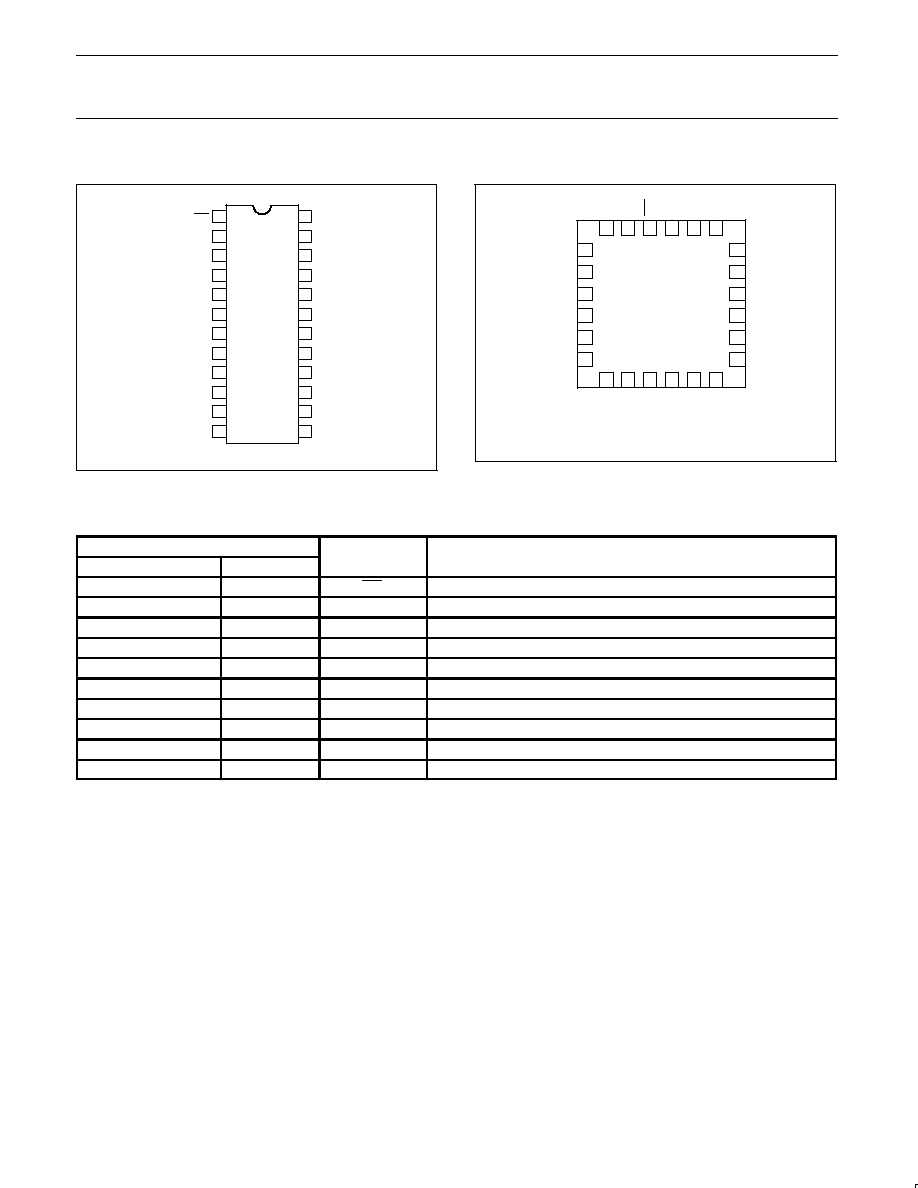
PIN CONFIGURATION -- DIP, SO, SSOP, TSSOP
su01438
1
2
3
4
5
6
7
8
9
10
11
12
13
14
15
16
17
18
19
20
21
22
23
24
INT
A1
A2
I/O0.0
I/O0.1
I/O0.2
I/O0.3
I/O0.4
I/O0.5
I/O0.6
I/O0.7
V
DD
SDA
SCL
A0
I/O1.7
I/O1.6
I/O1.5
I/O1.3
I/O1.4
I/O1.2
I/O1.1
I/O1.0
V
SS
Figure 1. Pin configuration -- DIP, SO, SSOP, TSSOP
PIN CONFIGURATION -- HVQFN
18
17
16
15
14
7
8
9
10
11
1
2
3
4
5
24
23
22
21
20
su01683
TOP VIEW
I/O0.0
A0
6
13
12
19
I/O0.1
I/O0.2
I/O0.3
I/O0.4
I/O0.5
I/O1.3
I/O1.4
I/O1.5
I/O1.6
I/O1.7
I/O0.6
I/O0.7
I/O1.0
I/O1.1
I/O1.2
A2
A1
INT
V
SDA
SCL
DD
V
SS
Figure 2. Pin configuration -- HVQFN
PIN DESCRIPTION
PIN NUMBER
SYMBOL
FUNCTION
DIP, SO, SSOP, TSSOP
HVQFN
SYMBOL
FUNCTION
1
22
INT
Interrupt output (open-drain)
2
23
A1
Address input 1
3
24
A2
Address input 2
4≠11
1≠8
I/O0.0≠I/O0.7
I/O0.0 to I/O0.7
12
9
V
SS
Supply ground
13≠20
10≠17
I/O1.0≠I/O1.7
I/O1.0 to I/O1.7
21
18
A0
Address input 0
22
19
SCL
Serial clock line
23
20
SDA
Serial data line
24
21
V
DD
Supply voltage

Philips Semiconductors
Product data sheet
PCA9555
16-bit I
2
C and SMBus I/O port with interrupt
2004 Sep 30
5
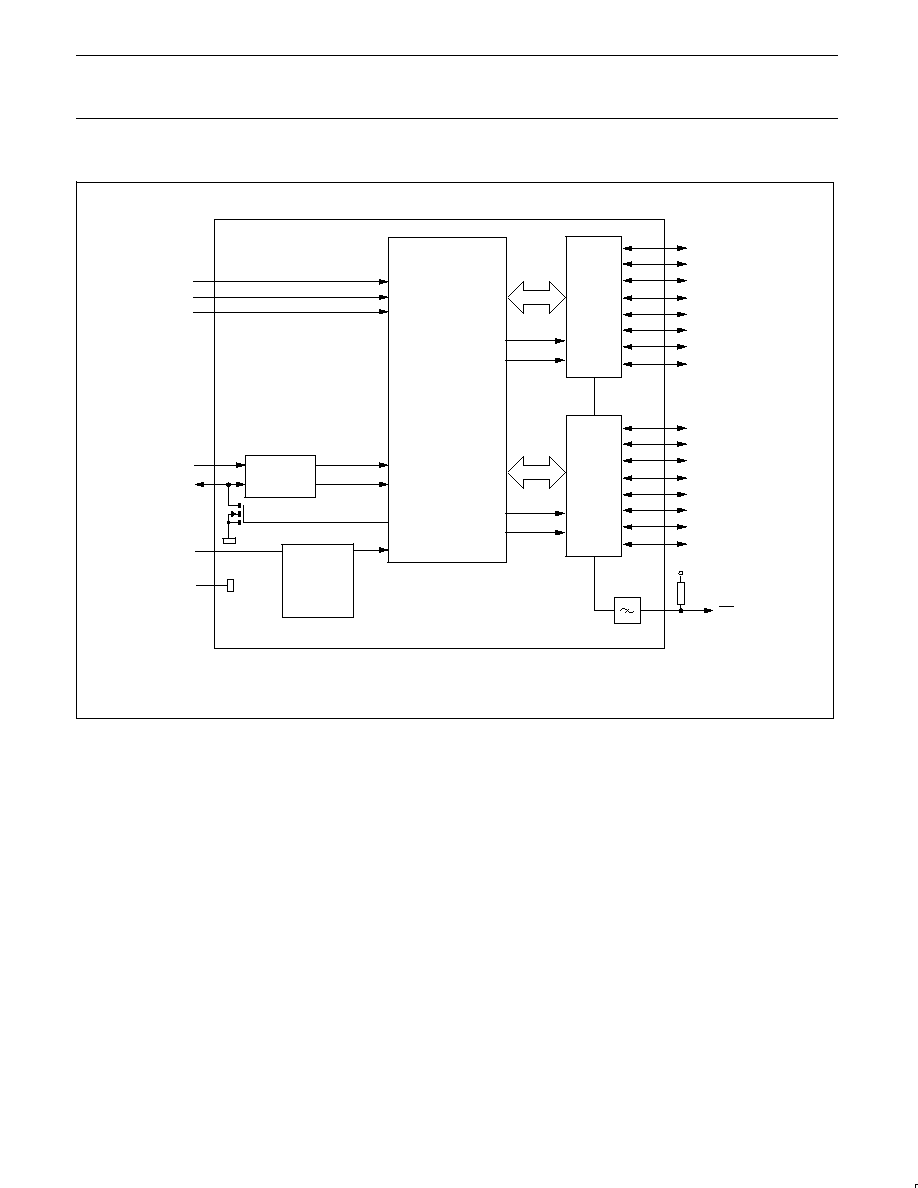
SIMPLIFIED SCHEMATIC OF I/Os
WRITE PULSE
DATA FROM
SHIFT REGISTER
V
DD
I/O PIN
V
SS
WRITE CONFIGURATION
PULSE
D
C
K
FF
Q
D
C
K
Q
FF
D
C
K
Q
FF
D
C
K
Q
FF
INPUT PORT
REGISTER
POLARITY
INVERSION
REGISTER
OUTPUT
PORT
REGISTER
DATA FROM
SHIFT REGISTER
DATA FROM
SHIFT REGISTER
WRITE
POLARITY
PULSE
CONFIGURATION
REGISTER
OUTPUT PORT
REGISTER DATA
INPUT PORT
REGISTER DATA
POLARITY
REGISTER DATA
READ PULSE
SU01473
Q
Q
Q
Q
TO INT
100 k
Q1
Q2
NOTE:
At Power-on Reset, all registers return to default values.
Figure 4. Simplified schematic of I/Os
I/O port
When an I/O is configured as an input, FETs Q1 and Q2 are off,
creating a high impedance input with a weak pull-up to V
DD
. The
input voltage may be raised above V
DD
to a maximum of 5.5 V.
If the I/O is configured as an output, then either Q1 or Q2 is on,
depending on the state of the Output Port register. Care should be
exercised if an external voltage is applied to an I/O configured as an
output because of the low impedance path that exists between the
pin and either V
DD
or V
SS
.