
PCD3316
Caller-ID on Call Waiting (CIDCW) receiver
11 March 1999
Product specification
c
c
Unrestr
icted
1.
General description
The PCD3316 is a low power mixed signal CMOS integrated circuit for receiving
physical layer signals like Bellcore's `CPE
1
Alerting Signal (CAS)' and the signals
used in similar services. The device is capable of a very high precision detection of
the dual tone (2130 and 2750 Hz) by using a patented digital algorithm. The
PCD3316 can be used for on-hook and off-hook Caller-ID (CID), Caller-ID on Call
Waiting (CIDCW) and Caller-Name (CNAM) applications.
For timing purposes the PCD3316 can be programmed to generate an interrupt
signal to the microcontroller every second or every minute. These timings are derived
from an on-chip 32.768 kHz oscillator.
Also incorporated in the device are a Frequency Shift Keying (FSK)
receiver/demodulator and a `Ring or polarity change detector'. The status of the
PCD3316, the received FSK data bytes and the ringer period can be read and many
options can be selected via the I
2
C-bus serial interface. Two on-chip oscillators are
available. One 3.58 MHz oscillator for all internal functions and a low frequency
32.768 kHz oscillator for the 1 second or 1 minute timing.
In Power-down mode only the polarity comparators and the 32.768 kHz oscillator are
active. The CAS detection, the FSK receiver and the 3.58 MHz oscillator can be
enabled separately. Detection of a polarity change on the inputs POL0 or POL1, the
reception of an FSK data byte, the detection of a CAS tone or a timebase interrupt is
signalled to the microcontroller by an interrupt request signal (IRQ). The
microcontroller can communicate with the PCD3316 device via the serial interface.
The PCD3316 is designed for use in a microcontroller controlled system. The device
is available in a SO16 package.
A demonstration board OM5843 and an application note
AN98071 are available.
1.
CPE = Customer Premises Equipment.

Philips Semiconductors
PCD3316
CIDCW receiver
Product specification
11 March 1999
2 of 30
9397 750 04824
� Philips Electronics N.V. 1999. All rights reserved.
Unrestr
icted
2.
Features
s
Bellcore's `CPE Alerting Signal (CAS)' and British Telecom's (BT) `Loop State
Tone Alert Signal' detection
s
BT's `Idle State Tone Alert Signal' by means of monitoring the input signal level
s
1200 baud FSK demodulator conform Bell 202 and CCITT V23 standards
s
Ring or polarity change detector
s
Ring period measurement
s
Low battery comparator
s
Signal level detector
s
On-hook and off-hook applications according to
Bellcore TR-NWT-000030 and
SR-TSV-002476 specifications
s
Receive sensitivity of
-
37.8 dBm (in 600
) for CAS
s
2.5 to 3.6 V supply; low power standby mode
s
Selectable 1 second or 1 minute timebase interrupt
s
3.58 MHz and 32.768 kHz crystal oscillators
s
SO16 package.
3.
Applications
s
Analog Display Services Interface (ADSI) phones
s
Feature phones and adjunct boxes with Bellcore CID, CIDCW and CNAM systems
s
Computer Telephony Integrated (CTI) systems.
4.
Ordering information
Table 1:
Ordering information
Type number
Package
Name
Description
Version
PCD3316T
SO16
plastic small outline package; 16 leads; body width 7.5 mm
SOT162-1

Philips Semiconductors
PCD3316
CIDCW receiver
Product specification
11 March 1999
3 of 30
9397 750 04824
� Philips Electronics N.V. 1999. All rights reserved.
Unrestr
icted
5.
Block diagram
6.
Pinning information
6.1 Pinning
Fig 1.
Block diagram.
handbook, full pagewidth
MBH983
3.58 MHz
OSCILLATOR
TIMING
PREPROCESSOR
PCD3316
LEVEL
DETECT
POR
TIME
BASE
VOLTAGE
REFERENCE
CAS
I
2
C-BUS
INTERFACE
32.768 kHz
OSCILLATOR
CONTROL
FSK
4
5
6
LXIN
LXOUT
SDA
SCL
7
3
IRQ
VDD
DGND
12
16
11
10
8
9
AGND
1
HXIN
13
CASIN
14
FSKIN
-
15
FSKIN
+
2
HXOUT
LOWBAT
POL0
POL1
Fig 2.
Pin configuration.
handbook, halfpage
MBH980
1
2
3
4
5
6
7
8
16
15
14
13
12
11
10
9
PCD3316
HXIN
VDD
HXOUT
FSKIN
+
IRQ
FSKIN
-
SCL
CASIN
SDA
LOWBAT
LXIN
POL0
LXOUT
POL1
DGND
AGND

Philips Semiconductors
PCD3316
CIDCW receiver
Product specification
11 March 1999
4 of 30
9397 750 04824
� Philips Electronics N.V. 1999. All rights reserved.
Unrestr
icted
6.2 Pin description
7.
Functional description
7.1 Preprocessor and analog inputs
The preprocessor for the CAS detection and the FSK receiver incorporates an
Analog-to-Digital Converter (ADC) and a digital bandpass filter.
The LOWBAT input of the PCD3316 can be used for low battery detection. The
voltage on the LOWBAT pin is compared with an internal voltage reference circuit.
When the LOWBAT voltage drops below the reference voltage, the Status register,
bit 5 is set to logic 1.
The PCD3316 can be forced in a Power-down state by switching off the 3.58 MHz
system clock and the ADC. This is done by setting Mode register 2, bit 7 (CIDMD2.7)
to logic 0. To guarantee correct operation the following order of actions must be
performed (see also
Section 7.8
about interrupts):
1. Switch off CAS and FSK detection (if turned on)
2. Read the interrupt register (thus clearing pending interrupts generated by the
CAS and FSK detector)
3. Switch off the 3.58 MHz oscillator by clearing bit 7 of Mode register 2.
The two low power comparators (inputs POL0 and POL1) and the 32.768 kHz clock
are always active.
Table 2:
Pin description
Symbol
Pin
I/O
Description
HXIN
1
I
3.58 MHz crystal oscillator input
HXOUT
2
O
3.58 MHz crystal oscillator output
IRQ
3
O
interrupt output; programmable active HIGH or active LOW
SCL
4
I
serial clock line of I
2
C-bus
SDA
5
I/O
serial data line of I
2
C-bus
LXIN
6
I
32.768 kHz crystal oscillator input
LXOUT
7
O
32.768 kHz crystal oscillator output
DGND
8
-
digital ground
AGND
9
-
analog ground
POL1
10
I
polarity detector input 1
POL0
11
I
polarity detector input 0
LOWBAT
12
I
low battery detector input
CASIN
13
I
input pin for CAS signal
FSKIN
-
14
I
negative input for FSK signal
FSKIN+
15
I
positive input for FSK signal
V
DD
16
-
supply

Philips Semiconductors
PCD3316
CIDCW receiver
Product specification
11 March 1999
5 of 30
9397 750 04824
� Philips Electronics N.V. 1999. All rights reserved.
Unrestr
icted
They can be used for ring or line polarity reversal detection. The POL on/off bit (Mode
register 1, bit 4) must be set to enable generation of an interrupt when a polarity
change occurs. The result of the two comparators can be read in bits 7 and 6 (POL0
and POL1) of the Status register (see
Section 7.4
). The 3.58 MHz clock is not needed
for the generation of a polarity interrupt.
7.2 CAS detection
After a power-on reset or after enabling the CAS detector the internal registers of the
CAS detection function are initialized. The initialization takes a maximum of
100 periods of the 3.58 MHz clock.
If the CAS detection is enabled the PCD3316 will generate an interrupt (Interrupt
register, bit 1 is set) when a correct dual tone (2130 and 2750 Hz) is detected.
Interrupts will be blocked when the signal level on the CAS input is below the
threshold in the level detector.
7.3 FSK reception
The FSK receiver function can be enabled by setting the FSK on/off bit (Mode
register 1, bit 7).
In the FSK transmission specification of BT and Bellcore a channel seizure is
transmitted first (sequence of 1010..). After the channel seizure a block of marks and
finally the data pattern are sent (see
Figure 3
). These mark bits are detected by the
PCD3316 which sets the FSK-BOM Indication bit (Status register, bit 4). The
FSK-BOM Indication bit is reset when the FSK receiver is disabled.
If the FSK-BOM Indication bit is set, the FSK receiver will generate an interrupt after it
has received a complete data word. An FSK data word consists of one start bit
(space), followed by eight data bits and one stop bit (mark). Interrupts will therefore
not be generated during the channel seizure and during the block of marks. When a
valid data word has been received, FSK data is available in the FSK data register.
By clearing the FSK-BOM-mask on/off bit (Mode register 1, bit 6), the FSK receiver
will not wait with the generation of interrupts until a Begin Of Mark (BOM) has been
detected but will handle the channel seizure as normal data. The block of marks
which is a string of logic 1 will still not generate interrupts because there are no start
bits.
After the generation of an interrupt the IRQ pin will become active (see
Figure 4
), and
the FSK Interrupt bit is set (Interrupt register, bit 5). The received data is available in
the FSK data register.
Fig 3.
FSK transmission specification.
width
MBH979
channel seizure
mark
FSK transmission
FSK-BOM
data

Philips Semiconductors
PCD3316
CIDCW receiver
Product specification
11 March 1999
6 of 30
9397 750 04824
� Philips Electronics N.V. 1999. All rights reserved.
Unrestr
icted
The FSK-OVR Error bit (Status register, bit 3) indicates that a previous byte is lost
due to an overrun. The FSK-FRM Error bit (Status register, bit 2) indicates an
incorrect start- or stop-bit. These frame errors indicate that there are synchronization
problems. The on-chip level detector can be used to detect a carrier loss during FSK
transmission. FSK data can be rejected when the signal level is below the reference
level, this to avoid that noise is interpreted as data (Interrupt register, bit 4 is logic 1).
7.4 Ring or polarity change detector
For ring and polarity change detection two comparators are available in the
PCD3316. The reference level of the comparators is set internally by the reference
voltage generator. The voltage levels on the two polarity comparator inputs, POL0
and POL1, are compared with the reference voltage V
ref
. If POL0 < V
ref
or
POL1 > V
ref
, POL0 and POL1 (Status register, bit 7 and 6) are set respectively and
reset if POL0 > V
ref
and POL1 < V
ref
. Every time the POL0 status bit changes from
logic 1 to logic 0, a POL0 interrupt is generated. Every time the POL1 status bit
changes from logic 0 to logic 1, a POL1 interrupt is generated.
The period time of a POL1-POL0-POL1 sequence is available in the Ringer period
register. It is preset to 255 on power-on and updated every time a POL1 interrupt is
generated. The sequence is:
1. Power-on: Ringer period register = 255
2. First POL1 interrupt: Ringer period register = 255
3. First POL1 interrupt after a POL0 interrupt: Ringer period register = new time
4. First POL1 interrupt after more than
255
/
2048
s: Ringer period register = 255.
The period is given in multiples of
1
/
2048
s. The maximum value is 255.
The POL1-POL0-POL1 sequence is recognized when one or more POL1 interrupts
are generated followed by one or more POL0 interrupts, followed by a POL1 interrupt.
The 32.768 kHz clock is needed for the generation of a polarity interrupt.
7.5 Low battery detection
The low battery voltage detection input (pin LOWBAT) is connected to the positive
input of a comparator. The negative input is connected to the internal reference
voltage. If the voltage on the LOWBAT input pin is less than the reference voltage V
ref
,
the LOW-BAT Indication (Status register, bit 5) is set. If the LOWBAT input rises
above V
ref
again, the LOW-BAT Indication is cleared.
Fig 4.
IRQ generation after reading a valid data byte.
handbook, full pagewidth
MBH981
START
IRQ
read by
serial interface
D0
D1
D2
D3
D4
D5
D6
D7
STOP

Philips Semiconductors
PCD3316
CIDCW receiver
Product specification
11 March 1999
7 of 30
9397 750 04824
� Philips Electronics N.V. 1999. All rights reserved.
Unrestr
icted
The 32.768 kHz clock signal must be available. The LOW-BAT Indication bit does not
generate interrupts, thus the bit should be polled.
7.6 Level detect
When the input signal level on the FSK or the CAS input (the one that is selected) is
below a threshold of typically
-
40 dBm, the Low Level Status bit will be set (Interrupt
register, bit 4). The level detector can be used to observe a carrier loss during FSK
transmission and to detect the `Idle State Tone Alert Signal' for British Telecom. The
signal power on the input can be monitored by polling the register bit since it will not
generate an interrupt. Signal power is measured in a frequency band corresponding
to the selected operation mode, FSK (1000 to 2200 Hz) or CAS (2000 to 2800 Hz).
The Low Level Status bit will be updated every 8 ms. When FSK and CAS are both
disabled the signal level on the FSK input is measured. The 32.768 kHz clock signal
must be available.
7.7 Time base
The 32.768 kHz oscillator is used to generate either a 1 second or a 1 minute
interrupt signal. If the TB on/off bit is set (Mode register 2, bit 6) every second or
minute an interrupt is generated and MIN Interrupt and/or SEC Interrupt bits
(Interrupt register, bit 7 and 6) are set. After reading the Interrupt register the interrupt
is cleared.
The SEC/MIN (Mode register 2, bit 5) selects whether every second (SEC/MIN is set)
or every minute (SEC/MIN is cleared) an interrupt is generated. All possible
selections are shown in
Table 3
. Resetting bit TB on/off in Mode register 2 (bit 6) will
only disable time base interrupts, and the 32.768 kHz oscillator will continue to run.
7.8 Interrupt
The interrupt request output (IRQ) is active HIGH by default. The polarity of the IRQ
output can be made active LOW by the INT Polarity HIGH/LOW bit (Mode register 1,
bit 3). The IRQ pin is in 3-state when not active, so an external pull-up or pull-down
resistor is required. The interrupt cause is indicated by the flags in the Interrupt
register. Interrupt flags are set by hardware but must be reset by software. All flags of
the Interrupt register are reset when the register is read via I
2
C-bus interface.
The IRQ pin is deactivated at the positive edge of SCL which reads the first data bit of
the Interrupt register. The IRQ pin will stay inactive for one SCL cycle. IRQ can
handle a next interrupt after the next positive edge of SCL.
[1]
X = don't care.
Table 3:
Selection of interrupt modes
Mode register 2 (CIDMD2)
Interrupt register (CIDINT)
Interrupt
TB on/off
(CIDMD2.6)
SEC/MIN
(CIDMD2.5)
MIN Interrupt
(CIDINT.7)
SEC Interrupt
(CIDINT.6)
0
X
[1]
0
0
no time base interrupt (time base is reset)
1
0
1
0
every minute an interrupt is generated; no second interrupt
1
1
1
1
every second an interrupt is generated; every minute an
interrupt is generated
Philips Semiconductors
PCD3316
CIDCW receiver
Product specification
11 March 1999
8 of 30
9397 750 04824
� Philips Electronics N.V. 1999. All rights reserved.
Unrestr
icted
7.9 The internal Power-on reset (POR)
The device contains an on-chip Power-on reset circuitry which activates a reset as
long as V
DD
is below a predefined level V
POR(H)
. If V
DD
exceeds V
POR(H)
, the
3.58 MHz oscillator will start. The PCD3316 is initialized and the internal registers are
set to the default value (see
Section 7.13
). It takes a maximum of 100 cycles of the
3.58 MHz clock to initialize all internal functions. The POR circuitry also ensures, that
the chip will be switched off as soon as a falling V
DD
reaches a predefined level
(V
POR(L)
).
7.10 3.58 MHz oscillator circuitry
The 3.58 MHz oscillator is needed for the FSK receiver and the CAS detection. This
on-chip Amplitude Controlled Oscillator (ACO) circuitry is a single-stage inverting
amplifier biased by an internal feedback resistor R
fb
. The oscillator circuit is shown in
Figure 5
. When using a quartz resonator to drive the oscillator, normally no external
components are needed.
When using ceramic resonators to drive the oscillator, in some cases external
components are needed; refer to the ceramic resonator product specifications. Two
different configurations are shown in
Figure 6a
and
Figure 6b
.
To drive the device with an external clock source, apply the external clock signal to
HXIN, and leave HXOUT to float, as shown in
Figure 6c
. If the amplitude of the input
signal is less than V
DD
to DGND or a sine wave is applied, capacitive decoupling is
needed as shown in
Figure 6d
.
In the Power-down mode (Mode register 2, bit 7 = 0), the oscillator is stopped and
HXIN and HXOUT are internally pulled LOW. The current of the whole oscillator is
switched off.
Fig 5.
Oscillator.
handbook, halfpage
MGK723
C1i
C1e
C2i
C2e
Rfb
AMPLITUDE
CONTROL
on/off
PCD3316
HXOUT
HXIN
1
2

Philips Semiconductors
PCD3316
CIDCW receiver
Product specification
11 March 1999
9 of 30
9397 750 04824
� Philips Electronics N.V. 1999. All rights reserved.
Unrestr
icted
a.
Standard oscillator: quartz or PXE.
b.
Oscillator: quartz or PXE with external capacitors.
c.
External clock: square wave.
d.
External clock: sine wave.
Fig 6.
3.58 MHz oscillator configurations.
handbook, halfpage
MGK725
HXIN
1
HXOUT
2
PCD3316
handbook, halfpage
MGK726
HXIN
1
C1e
C2e
HXOUT
2
PCD3316
handbook, halfpage
MGK727
HXIN
3.58 MHz
square wave
1
HXOUT
2
PCD3316
handbook, halfpage
MGK728
HXIN
3.58 MHz
sine wave
1
HXOUT
2
PCD3316
C1
e
and C2
e
are the external load capacitances
(see
Figure 6b
). Normally, they are not needed
due to integrated load capacitances of 10 pF;
see curve (2).
(1)
C1
e
= C2
e
= 22 pF.
(2)
C1
e
= C2
e
= 0 pF.
(3)
C1
e
= C2
e
= 12 pF.
For correct function of the oscillator, the values
of R1 and C0 of the chosen resonator (quartz or
PXE) must be below the related curve lines
shown in
Figure 7a
. The value of the parallel
resistor R0 must be less than 47 k
.
The wiring between chip and resonator should
be kept as short as possible.
a.
Resonator requirements for the ACO.
b.
Resonator equivalent circuit.
Fig 7.
Resonator requirements and equivalent circuit.
handbook, halfpage
0
(1)
(2)
C0 (pF)
20
40
80
500
0
R1
(
)
400
60
300
200
100
MBK948
(3)
handbook, halfpage
C1
C0
L1
R1
R0
MBK947

Philips Semiconductors
PCD3316
CIDCW receiver
Product specification
11 March 1999
10 of 30
9397 750 04824
� Philips Electronics N.V. 1999. All rights reserved.
Unrestr
icted
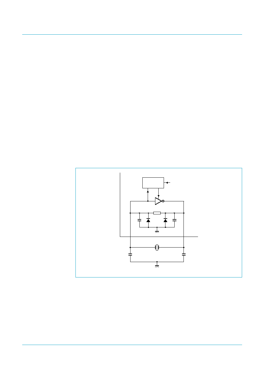
7.11 32 kHz oscillator
The 32.768 kHz oscillator is enabled permanently and is used to generate either a
1 second or 1 minute interrupt. The 32.768 kHz clock is also used for the `Ring or
polarity change detector', the `Low battery detection' and the `Level detect' function.
An external 32.768 kHz signal may be applied to pin LXIN while leaving pin LXOUT
not connected.
The 32 kHz oscillator requires an external 32.768 kHz quartz crystal and an external
feedback resistor (4.7 M
) between the LXIN and LXOUT pins (see
Figure 8
).
7.12 Serial interface
The serial interface of the PCD3316 is the I
2
C-bus. A detailed description of the
I
2
C-bus specification, including applications, is given in the brochure:
The I
2
C-bus
and how to use it, order no. 9398 393 40011 or I
2
C Peripherals Data Handbook IC12.
7.12.1
Characteristics of the I
2
C-bus
For the I
2
C-bus configuration see
Figure 9
. A device generating a message is a
`transmitter', a device receiving a message is the `receiver'. The device that controls
the message is the `master' and the devices which are controlled by the master are
called the `slaves'. The PCD3316 operates in the slave transmitter/receiver mode
only.
The I
2
C-bus is for bidirectional, two-line communication between different ICs or
modules. The two lines are a serial data line (SDA) and a serial clock line (SCL). Both
lines must be connected to a positive supply via a pull-up resistor. Data transfer may
be initiated only when the bus is not busy.
Fig 8.
Connections of the 32 kHz oscillator.
handbook, halfpage
MGK724
32.768 kHz
32.768 kHz
OSCILLATOR
LXIN
LXOUT
PCD3316
6
7
4.7 M

Philips Semiconductors
PCD3316
CIDCW receiver
Product specification
11 March 1999
11 of 30
9397 750 04824
� Philips Electronics N.V. 1999. All rights reserved.
Unrestr
icted
7.12.2
START and STOP conditions
Both data and clock lines remain HIGH when the bus is not busy. A HIGH-to-LOW
transition of the data line, while the clock is HIGH is defined as the START condition
(S). A LOW-to-HIGH transition of the data line while the clock is HIGH is defined as a
STOP condition (P); see
Figure 10
.
7.12.3
Bit transfer
One data bit is transferred during each clock pulse. The data on the SDA line must
remain stable during the HIGH period of the clock pulse as changes in the data line at
this time will be interpreted as a control signal; see
Figure 11
.
7.12.4
Acknowledge
The number of data bytes transferred between the START and the STOP conditions
from the transmitter to the receiver is unlimited. Each byte of eight bits is followed by
an acknowledge bit. The acknowledge bit is a HIGH level signal put on the bus by the
transmitter during which time the master generates an extra acknowledge-related
clock pulse.
A slave receiver which is addressed must generate an acknowledge after the
reception of each byte. Also a master receiver must generate an acknowledge after
the reception of each byte that has been clocked out of the slave transmitter.
Fig 9.
I
2
C-bus configuration.
MBA605
MASTER
TRANSMITTER /
RECEIVER
SLAVE
RECEIVER
SLAVE
TRANSMITTER /
RECEIVER
MASTER
TRANSMITTER
MASTER
TRANSMITTER /
RECEIVER
SDA
SCL
Fig 10. START and STOP conditions for the I
2
C-bus.
MBA608
SDA
SCL
P
STOP condition
SDA
SCL
S
START condition
Fig 11. I
2
C-bus bit transfer.
MBA607
data line
stable;
data valid
change
of data
allowed
SDA
SCL

Philips Semiconductors
PCD3316
CIDCW receiver
Product specification
11 March 1999
12 of 30
9397 750 04824
� Philips Electronics N.V. 1999. All rights reserved.
Unrestr
icted
The device that acknowledges must pull down the SDA line during the acknowledge
clock period immediately after the 8th SCL pulse, so that the SDA line is stable LOW
during the HIGH period of the acknowledge related clock pulse (set-up and hold
times must be taken into consideration).
A master receiver must signal an end of data to the transmitter by not generating an
acknowledge on the last byte that has been clocked out of the slave. In this event the
transmitter must leave the data line HIGH to enable the master to generate a STOP
condition.
7.12.5
I
2
C-bus protocol
Before any data is transmitted on the I
2
C-bus, the device which should respond is
addressed first. The addressing is always carried out with first byte transmitted after
the START procedure. One I
2
C-bus slave address is reserved for the PCD3316, E0H
(1110 0000 for write and 1110 0001 for read).
The I
2
C-bus protocol is shown in
Figure 13
. Two different sequences are considered,
the write sequence and the read sequence. Both sequences are initiated with a
START condition (S) from the I
2
C-bus master which is followed by the PCD3316 slave
address with the read bit cleared. The first byte after the I
2
C-bus address is
interpreted as the address of a PCD3316 register.During the write sequence the
register address of the PCD3316 is auto-incremented on each acknowledge. The
write sequence is ended with a STOP condition from the master. If the addressed
register is read-only or non-existent, nothing will be changed.
For the read sequence the bus master issues a repeated START condition followed
by the PCD3316 slave address with the read bit set. Then data is read from
previously set address and sent out. When the master responds with an acknowledge
the address of the register is auto incremented and the slave will put the data from
the next register on the bus. The read sequence is stopped when the master stops
giving an acknowledge and generates a STOP condition.
When a non-existing register is addressed the PCD3316 will return FFH. Existing
register addresses are shown in
Section 7.13
. An additional register address (73H) is
reserved for test purposes. This address cannot be reached with the auto-increment
function of the I
2
C-bus interface.
Fig 12. I
2
C-bus acknowledge.
idth
MBC602
S
START
condition
9
8
2
1
clock pulse for
acknowledgement
not acknowledge
acknowledge
DATA OUTPUT
BY TRANSMITTER
DATA OUTPUT
BY RECEIVER
SCL FROM
MASTER

Philips Semiconductor
s
PCD3316
CIDCW receiver
Pr
oduct specification
11 Mar
c
h
1999
13 of 30
9397 750 04824
� Philips Electronics N.V
. 1999. All r
ights reser
v
ed.
Unrestr
icted
a.
I
2
C-bus write sequence.
b.
I
2
C-bus read sequence.
Fig 13. I
2
C-bus write and read sequence.
handbook, full pagewidth
S
0 A
SLAVE ADDRESS
REGISTER ADDRESS
A
A
DATA
acknowledgement
from slave
acknowledgement
from slave
acknowledgement
from slave
R/W
auto increment
word address
MBH975
n bytes
P
S
0 A
SLAVE ADDRESS
REGISTER ADDRESS
A
A
SLAVE ADDRESS
acknowledgement
from slave
acknowledgement
from slave
acknowledgement
from slave
R/W
acknowledgement
from master
A
DATA
auto increment
register address
MBH976
P
no acknowledgement
from master
1
DATA
R/W
S
1
n bytes
auto increment
register address
n bytes
at this moment master-
transmitter becomes
master - receiver and
PCD3316 slave-receiver
becomes slave-transmitter

Philips Semiconductors
PCD3316
CIDCW receiver
Product specification
11 March 1999
14 of 30
9397 750 04824
� Philips Electronics N.V. 1999. All rights reserved.
Unrestr
icted
7.12.6
I
2
C-bus bit rate
When a microcontroller is used that implements an I
2
C-bus in software, the bit rate of
the I
2
C-bus can be critical during reception of FSK. The collection of the interrupt
data and FSK-data from the PCD3316 takes 48 bits on the I
2
C-bus. With an FSK
baud rate of 1200 (corresponds to 1200 bits per second) the minimal speed of the
I
2
C-bus should be 5.76 kbits/s. Additional interrupts generated by the time base of the
PCD3316 will cause the processor to collect extra information from the PCD3316.
As a consequence, the FSK-data can be overrun in the PCD3316 and one data byte
will be lost. In this case, the time base interrupt should be suppressed while FSK is
active. This can be done by setting the `INT-SUP on/off' bit (bit 4 in Mode register 2).
The `TB on/off' bit (bit 6 in Mode register 2) will still be set but the IRQ output will not
be activated by the time base interrupt. Any time base interrupt can be detected by
the microcontroller when an FSK interrupt is processed by reading the Interrupt
register.

Philips Semiconductors
PCD3316
CIDCW receiver
Product specification
11 March 1999
15 of 30
9397 750 04824
� Philips Electronics N.V. 1999. All rights reserved.
Unrestr
icted
7.13 Registers
7.13.1
Interrupt register (CIDINT)
Table 4:
Register overview
Address
Name
Function
Read/Write
Default value
00H
CIDINT
Interrupt register
read only
0000 0000
01H
CIDFSK
FSK data register
read only
-
02H
CIDSTA
Status register
read only
-
03H
CIDRNG
Ringer period register
read only
-
04H
CIDMD1
Mode register 1
read/write
0101 1000
05H
CIDMD2
Mode register 2
read/write
1101 0000
Table 5:
Interrupt register
Address: 00H; read only.
7
6
5
4
3
2
1
0
MIN Interrupt
SEC Interrupt
FSK Interrupt
Low Level Status
POL1 Interrupt
POL0 Interrupt
CAS Interrupt
-
Table 6:
Description of CIDINT bits
Bit
Symbol
Description
CIDINT.7 MIN Interrupt
MIN Interrupt = 0: no interrupt request;
MIN Interrupt = 1: one minute interrupt request
CIDINT.6 SEC Interrupt
SEC Interrupt = 0: no interrupt request;
SEC Interrupt = 1: one second interrupt request
CIDINT.5 FSK Interrupt
FSK Interrupt = 0: no FSK interrupt or FSK disabled;
FSK Interrupt = 1: FSK interrupt, one byte received
CIDINT.4 Low Level Status Low Level Status = 0: signal level on selected input above power reference (no interrupt);
Low Level Status = 1: signal level on selected input below power reference (no interrupt)
CIDINT.3 POL1 Interrupt
POL1 Interrupt = 0: no zero to one changes on POL1 input or polarity interrupt disabled;
POL1 Interrupt = 1: a one to zero input change on the POL1 input is detected
CIDINT.2 POL0 Interrupt
POL0 Interrupt = 0: no one to zero changes on POL0 input or polarity interrupt disabled;
POL0 Interrupt = 1: a zero to one input change on the POL0 input is detected
CIDINT.1 CAS Interrupt
CAS Interrupt = 0: no CAS signal detected or CAS disabled;
CAS Interrupt = 1: CAS signal detected
CIDINT.0
-
reserved bit

Philips Semiconductors
PCD3316
CIDCW receiver
Product specification
11 March 1999
16 of 30
9397 750 04824
� Philips Electronics N.V. 1999. All rights reserved.
Unrestr
icted
7.13.2
FSK data register (CDFSK)
7.13.3
Status register (CIDSTA)
7.13.4
Ringer period register (CIDRNG)
Table 7:
Interrupt register
Address: 01H; read only.
7
6
5
4
3
2
1
0
D7
D6
D5
D4
D3
D2
D1
D0
Table 8:
Description of CDFSK bits
Bit
Symbol
Description
CDFSK.7 to
CDFSK.0
D7 to D0
If an FSK interrupt has occurred and no FSK error is detected, the FSK data register
contains valid data.
Table 9:
Status register
Address: 02H; read only.
7
6
5
4
3
2
1
0
POL1
POL0
LOW-BAT Indication
FSK-BOM Indication
FSK-OVR Error
FSK-FRM Error
-
-
Table 10: Description of CIDSTA bits
Bit
Symbol
Description
CIDSTA.7
POL1
POL1 = 0: voltage on input POL1 < V
ref
; POL1 = 1: voltage on input POL1 > V
ref
CIDSTA.6
POL0
POL0 = 0: voltage on input POL0 > V
ref
; POL0 = 1: voltage on input POL0 < V
ref
CIDSTA.5
LOW-BAT Indication LOW-BAT Indication = 0: voltage on input LOWBAT > V
ref
;
LOW-BAT Indication = 1: voltage on input LOWBAT < V
ref
CIDSTA.4
FSK-BOM Indication FSK-BOM Indication = 0: begin of mark period not yet detected;
FSK-BOM Indication = 1: begin of mark period detected
CIDSTA.3
FSK-OVR Error
FSK-OVR Error = 0: no FSK overrun error;
FSK-OVR Error = 1: FSK overrun error, data byte(s) lost
CIDSTA.2
FSK-FRM Error
FSK-FRM Error = 0: no FSK frame error;
FSK-FRM Error = 1: FSK frame error, stop bit was wrong
CIDSTA.1 and
CIDSTA.0
-
reserved bits
Table 11: Register format
Address: 03H; read only.
7
6
5
4
3
2
1
0
D7
D6
D5
D4
D3
D2
D1
D0
Table 12: Description of CIDRNG bits
Bit
Symbol
Description
CIDRNG.7 to
CIDRNG.0
D7 to D0
The value held in this byte denotes the time between two positive edges of the POL1
comparator output (between two positive edges of POL1 one positive edge of POL0
must have been detected).

Philips Semiconductors
PCD3316
CIDCW receiver
Product specification
11 March 1999
17 of 30
9397 750 04824
� Philips Electronics N.V. 1999. All rights reserved.
Unrestr
icted
7.13.5
Mode register 1 (CIDMD1)
7.13.6
Mode register 2 (CIDMD2)
Table 13: Mode register 1
Address: 04H; read/write.
7
6
5
4
3
2
1
0
FSK on/off
FSK-BOM-mask on/off
CAS on/off
POL on/off
INT polarity HIGH/LOW
-
-
-
Table 14: Description of CIDMD1 bits
Bit
Symbol
Description
CIDMD1.7
FSK on/off
FSK on/off = 0: FSK receiver disabled; FSK on/off = 1: FSK receiver enabled
CIDMD1.6
FSK-BOM-mask on/off
FSK-BOM-mask on/off = 0: FSK interrupts will be generated when a data word was
received even before mark period (data from channel seizure);
FSK-BOM-mask on/off = 1: FSK interrupts will only be generated after the mark
period was detected (no interrupts from channel seizure)
CIDMD1.5
CAS on/off
CAS on/off = 0: CAS detector disabled; CAS on/off = 1: CAS detector enabled
CIDMD1.4
POL on/off
POL on/off = 0: disable interrupts due to polarity change;
POL on/off = 1: enable interrupts due to polarity change
CIDMD1.3
INT polarity HIGH/LOW INT polarity HIGH/LOW = 0: interrupt pin active LOW;
INT polarity HIGH/LOW = 1: interrupt pin active HIGH
CIDMD1.2 to
CIDMD1.0
-
reserved bits
Table 15: Mode register 2
Address: 05H; read/write.
7
6
5
4
3
2
1
0
XTAL on/off
TB on/off
SEC/MIN
INT-SUP on/off
-
-
-
-
Table 16: Description of CIDMD2 bits
Bit
Symbol
Description
CIDMD2.7
XTAL on/off
XTAL on/off = 0: disable 3.58 MHz oscillator;
XTAL on/off = 1: enable 3.58 MHz oscillator
CIDMD2.6
TB on/off
TB on/off = 0: disable 32.768 kHz timebase;
TB on/off = 1: enable 32.768 kHz timebase
CIDMD2.5
SEC/MIN
SEC/MIN = 0: every minute a timebase interrupt;
SEC/MIN = 1: every second a timebase interrupt
CIDMD2.4
INT-SUP on/off
INT-SUP on/off = 0: enable SEC/MIN interrupts during FSK reception;
INT-SUP on/off = 1: disable SEC/MIN interrupts during FSK reception
CIDMD2.3 to
CIDMD2.0
-
reserved bits

Philips Semiconductors
PCD3316
CIDCW receiver
Product specification
11 March 1999
18 of 30
9397 750 04824
� Philips Electronics N.V. 1999. All rights reserved.
Unrestr
icted
8.
Limiting values
[1]
V
I(max)
= 5.0 V.
9.
Characteristics
Table 17: Limiting values
In accordance with the Absolute Maximum Rating System (IEC 60134).
Symbol
Parameter
Conditions
Min
Max
Unit
V
DD
supply voltage
-
0.5
+5.0
V
I
DD
supply current
-
50
mA
I
I
DC input current at any input
-
10
+10
mA
I
O
DC output current at any output
-
10
+10
mA
V
I
input voltage on all inputs
-
0.5
V
DD
+ 0.5
[1]
V
P
tot
total power dissipation
-
300
mW
P
O
power dissipation per output
-
10
mW
T
amb
operating ambient temperature
-
25
+70
�
C
T
stg
storage temperature
-
65
+150
�
C
Table 18: Characteristics
V
DD
= 2.5 to 3.6 V; T
amb
=
-
25 to +70
�
C; HXIN = 3.579545 MHz
�
0.05%; LXIN = 32.768 kHz
�
0.1%; unless otherwise
specified.
Symbol
Parameter
Conditions
Min
Typ
Max
Unit
V
DD
supply voltage
[1]
2.5
3.3
3.6
V
V
POR(H)
power-on reset HIGH voltage
1.85
2.05
2.25
V
V
hys(POR)
power-on reset hysteresis voltage
[2]
50
100
150
mV
I
DD
supply currents
V
DD
= 2.5 V
Power-down mode
[3]
-
30
70
�
A
operating
[3] [4]
-
2.0
2.3
mA
Low voltage and polarity comparators (pins LOWBAT, POL0 and POL1)
V
hys
hysteresis voltage
-
20
-
mV
I
LI
input leakage current
[5]
-
-
1
�
A
Internal reference
V
ref
reference voltage level
1.125
1.25
1.375
V
P
i(ref)
input signal reference power for Low
Level Status bit
in 600
load
[6]
-
43.8
-
-
37.8
dBm
t
r(level)
input signal to Low Level Status bit rise
time
input signal power < P
i(ref)
-
-
8
ms
t
f(level)
input signal to Low Level Status bit fall
time
input signal power > P
i(ref)
-
-
8
ms
Logical output (pin IRQ)
[7]
I
OL
LOW-level output current
V
IRQ
= 0.4 V
2
-
-
mA
I
OH
HIGH-level output current
V
IRQ
= V
DD
-
0.4 V
2
-
-
mA

Philips Semiconductors
PCD3316
CIDCW receiver
Product specification
11 March 1999
19 of 30
9397 750 04824
� Philips Electronics N.V. 1999. All rights reserved.
Unrestr
icted
FSK receiver (pins FSKIN+ and FSKIN
-
)
Z
i
input impedance FSKIN+ to FSKIN
-
-
1.4
-
M
Z
source(max)
maximum source impedance
-
-
200
k
P
i(FSKIN)
input signal power
in 600
load
[8]
-
50
-
0
dBm
S/N
FSK
signal-to-noise ratio
200 to 3400 Hz
20
-
-
dB
|
V
dif
|
differential voltage between mark and
space (twist)
-
-
10
dB
f
(D)
data transmission rate frequency
1180
1200
1212
bits/s
f
s
space frequency
2068
-
2222
Hz
f
m
mark frequency
1188
-
1320
Hz
CAS detector (pin CASIN)
Z
i
input impedance CASIN to V
ref
-
1.4
-
M
Z
source(max)
maximum source impedance
-
-
200
k
P
i
input signal power
in 600
load
[8]
-
37.8
-
0
dBm
TH
ns(CAS)
no signal threshold (CAS)
in 600
load
-
43.8
-
-
37.8
dBm
f
l
low tone frequency
-
2130
-
Hz
f
h
high tone frequency
-
2750
-
Hz
f
max
maximum frequency deviation
[9]
-
0.5
-
+0.5
%
V
dif
differential voltage level (twist)
[9]
-
-
6
dB
t
dt
dual tone detection time
60
-
-
ms
I
2
C-bus interface (pins SCL and SDA)
[10]
; see
Figure 14
V
IL
LOW-level input voltage
[11]
0
-
0.3V
DD
V
V
IH
HIGH-level input voltage
[11]
0.7V
DD
-
V
DD
V
I
OL1
LOW-level output current for pin SDA
V
O(SDA)
= 0.4 V
2
-
-
mA
C
i
input capacitance for each I/O pin
-
-
10
pF
f
SCL
SCL clock frequency
-
-
100
kHz
t
BUF
bus free time
4.7
-
-
�
s
t
SU;STA
START condition set-up time
4.7
-
-
�
s
t
HD;STA
START condition hold time
4.0
-
-
�
s
t
LOW
SCL LOW time
4.7
-
-
�
s
t
HIGH
SCL HIGH time
4.0
-
-
�
s
t
r
maximum SCL and SDA rise time
[12]
-
-
1000
ns
t
f
maximum SCL and SDA fall time
[12]
-
-
300
ns
t
SU;DAT
data set-up time
250
-
-
ns
t
HD;DAT
data hold time
0
-
-
ns
t
VD;DAT
SCL LOW to data out valid time
-
-
3.4
�
s
t
SU;STO
STOP condition set-up time
4.0
-
-
�
s
Table 18: Characteristics
...continued
V
DD
= 2.5 to 3.6 V; T
amb
=
-
25 to +70
�
C; HXIN = 3.579545 MHz
�
0.05%; LXIN = 32.768 kHz
�
0.1%; unless otherwise
specified.
Symbol
Parameter
Conditions
Min
Typ
Max
Unit

Philips Semiconductors
PCD3316
CIDCW receiver
Product specification
11 March 1999
20 of 30
9397 750 04824
� Philips Electronics N.V. 1999. All rights reserved.
Unrestr
icted
[1]
Except for FSK and CAS detection, all circuitry works already when V
DD
> V
POR(H)
. Since the I
2
C-bus interface will work (starts to
acknowledge), the application can start reading the LOW-BAT Indication bit (Status register, bit 5) to check whether the supply voltage
has reached the operating voltage level. A voltage divider network can be connected to pins V
DD
, LOWBAT and AGND/DGND such that
V
LOWBAT
= V
ref
if V
DD
= V
DD(min)
.
[2]
The power-on reset LOW level is defined as V
POR(L)
= V
POR(H)
-
V
hys(POR)
. By design V
POR(L)
is always lower than V
POR(H)
.
[3]
32 kHz oscillator on (MIN Interrupt, SEC Interrupt, Polarity change, Low battery and Level detect available).
[4]
3.58 MHz oscillator on (device fully operational).
[5]
GND < V
I
< V
DD
. The leakage currents are generally very small, <1 nA. The value given here, 1
�
A, is a maximum that can occur after
an Electrostatic Stress on the pin.
[6]
When FSK is selected the signal power is measured between 1000 and 2200 Hz. When CAS is selected signal levels are measured
between 2000 and 2800 Hz.
[7]
The IRQ pin is implemented as a 3-state pin which is only active (either HIGH or LOW) when an interrupt occurs. A pull-up or pull-down
has to be connected to define the line when no interrupt is generated.
[8]
Verified on sampling basis.
[9]
According to Bellcore specification: near end speech level
-
7 dBm ASL (ASL = Active Speech Level), referenced to 600
, according
to method B of recommendation P.56.
[10] Pins SCL and SDA are equipped with an open-drain output buffer. The pins have no clamp diode to V
DD
.
[11] The input threshold voltage of SCL and SDA meet the I
2
C-bus specification. Therefore, an input voltage below 0.3V
DD
will be recognized
as a logic 0 and an input voltage above 0.7V
DD
will be recognized as a logic 1
[12] Maximum capacitive load for each bus line is 400 pF.
[13] C1
i
and C2
i
are the total internal capacitances (including gate capacitance and leadframe capacitance).
3.58 MHz oscillator (pins HXIN and HXOUT)
V
HXIN(p-p)
external clock signal amplitude
(peak-to-peak value) on pin HXIN
0.5
-
V
DD
V
Z
i(HXIN)
input impedance on pin HXIN
300
1000
-
k
C1
i
; C2
i
input capacitance on pins HXIN and
HXOUT
[13]
-
10
-
pF
32 kHz oscillator (pins LXIN and LXOUT)
g
m
transconductance
V
i(p-p)
< 50 mV
2
4
10
�
S
C
i(LXIN)
LXIN input capacitance
-
13
-
pF
C
o(LXOUT)
LXOUT output capacitance
-
10
-
pF
Table 18: Characteristics
...continued
V
DD
= 2.5 to 3.6 V; T
amb
=
-
25 to +70
�
C; HXIN = 3.579545 MHz
�
0.05%; LXIN = 32.768 kHz
�
0.1%; unless otherwise
specified.
Symbol
Parameter
Conditions
Min
Typ
Max
Unit

Philips Semiconductors
PCD3316
CIDCW receiver
Product specification
11 March 1999
21 of 30
9397 750 04824
� Philips Electronics N.V. 1999. All rights reserved.
Unrestr
icted
a.
Timing diagram 1.
b.
Timing diagram 2.
Fig 14. I
2
C-bus timing.
handbook, full pagewidth
MBH977
tSU;STA
SCL
SDA
tHD;STA
tr
tf
tBUF
tLOW
tHIGH
tSU;DAT
tHD;DAT
1/fSCL
handbook, full pagewidth
MBH978
tVD;DAT
tSU;STO
SDA
SCL

Philips Semiconductor
s
PCD3316
CIDCW receiver
Pr
oduct specification
11 Mar
c
h
1999
22 of 30
9397 750 04824
� Philips Electronics N.V
. 1999. All r
ights reser
v
ed.
Unrestr
icted
10.
Application inf
ormation
A demo-board (OM5843) of this configuration is available. Please contact your Philips sales office.
(1)
See
Figure 16a
.
(2)
See
Figure 16b
.
Fig 15. Application diagram for a telephone with CID/CIDCW functionality.
k
, full pagewidth
MGK722
RINGER/
INTERRUPTER
TRANSMISSION IC
MICRO CONTROLLER
LCD
CID/CIDCW RECEIVER
PCD3316
ATTENNUATION
(1)
ATTENNUATION
(1)
CAS FILTER
(2)
32.768 kHz
3.58 MHz
LXIN
LXOUT
HXOUT
HXIN
BATTERIES
VDD
LOWBAT
2
2
POL1/0
FSKIN
+
/
-
CASIN
IRQ
TONE
VBAT
VDD
VBAT
QR
IRQ
KEYBOARD
VDD
VDD
fxtal
I
2
C-bus
a/b
b/a
CSI
TONE

Philips Semiconductors
PCD3316
CIDCW receiver
Product specification
11 March 1999
23 of 30
9397 750 04824
� Philips Electronics N.V. 1999. All rights reserved.
Unrestr
icted
11. Test information
11.1 Application note on Customer Premises Equipment (CPE) testing
Under certain circumstances, some external CIDCW test equipment may generate
incorrect pulses after the ringing signal becomes inactive. These pulses may cause
the FSK detector of the PCD3316 to respond. Note that this is by no means an
incorrect behaviour of the PCD3316 chip, but a correct detection of incorrect test
stimuli. However, if not known, it may lead to confusing results during testing of the
CPE.
To avoid the issue described above, following work-around can be used:
1. Disable the FSK detection of PCD3316, before and during the ringing signal
detection.
2. Switch on the FSK detection only after a certain period, e.g. 100 ms after the
ringing signal goes inactive.
3. When the first FSK data is detected, e.g `55H' (possible part of channel seizure),
switch off the FSK detection and on again. This will force the FSK detector to
resynchronize and detect the normal FSK data correctly. It may be necessary to
repeat this sequence a number of times to ensure that the data detected really
comes from the channel seizure. Thus, it is recommended to wait for a multiple
number of bytes `55H' to be detected to validate a correct channel seizure.
Attenuation networks to connect the polarity and FSK inputs to
the telephone line.
High-pass filter (cut-off
frequency
1 kHz) to improve
performance of CAS detection.
a.
Attenuation networks.
b.
High-pass filter.
Fig 16. Application diagrams.
MGK729
820 k
100 k
100 k
820 k
100 k
100 k
POL0
POL1
a/b
b/a
FSKIN
+
FSKIN
-
11
10
14
15
1 nF
1 nF
PCD3316
2.2
�
F
(250 V)
2.2
�
F
(250 V)
telephone
line
ook, halfpage
MBH996
CASIN
13
120 k
100 nF
1.8 nF
PCD3316

Philips Semiconductors
PCD3316
CIDCW receiver
Product specification
11 March 1999
24 of 30
9397 750 04824
� Philips Electronics N.V. 1999. All rights reserved.
Unrestr
icted
12. Package outline
Fig 17. SOT162-1.
UNIT
A
max.
A
1
A
2
A
3
b
p
c
D
(1)
E
(1)
(1)
e
H
E
L
L
p
Q
Z
y
w
v
REFERENCES
OUTLINE
VERSION
EUROPEAN
PROJECTION
ISSUE DATE
IEC
JEDEC
EIAJ
mm
inches
2.65
0.30
0.10
2.45
2.25
0.49
0.36
0.32
0.23
10.5
10.1
7.6
7.4
1.27
10.65
10.00
1.1
1.0
0.9
0.4
8
0
o
o
0.25
0.1
DIMENSIONS (inch dimensions are derived from the original mm dimensions)
Note
1. Plastic or metal protrusions of 0.15 mm maximum per side are not included.
1.1
0.4
SOT162-1
8
16
w
M
b
p
D
detail X
Z
e
9
1
y
0.25
075E03
MS-013AA
pin 1 index
0.10
0.012
0.004
0.096
0.089
0.019
0.014
0.013
0.009
0.41
0.40
0.30
0.29
0.050
1.4
0.055
0.419
0.394
0.043
0.039
0.035
0.016
0.01
0.25
0.01
0.004
0.043
0.016
0.01
X
A
A
1
A
2
H
E
L
p
Q
E
c
L
v
M
A
(A )
3
A
0
5
10 mm
scale
SO16: plastic small outline package; 16 leads; body width 7.5 mm
SOT162-1
95-01-24
97-05-22

Philips Semiconductors
PCD3316
CIDCW receiver
Product specification
11 March 1999
25 of 30
9397 750 04824
� Philips Electronics N.V. 1999. All rights reserved.
Unrestr
icted
13. Soldering
13.1 Introduction to soldering surface mount packages
This text gives a very brief insight to a complex technology. A more in-depth account
of soldering ICs can be found in our
Data Handbook IC26; Integrated Circuit
Packages (document order number 9398 652 90011).
There is no soldering method that is ideal for all surface mount IC packages. Wave
soldering is not always suitable for surface mount ICs, or for printed-circuit boards
with high population densities. In these situations reflow soldering is often used.
13.2 Reflow soldering
Reflow soldering requires solder paste (a suspension of fine solder particles, flux and
binding agent) to be applied to the printed-circuit board by screen printing, stencilling
or pressure-syringe dispensing before package placement.
Several methods exist for reflowing; for example, infrared/convection heating in a
conveyor type oven. Throughput times (preheating, soldering and cooling) vary
between 100 and 200 seconds depending on heating method.
Typical reflow peak temperatures range from 215 to 250
�
C. The top-surface
temperature of the packages should preferable be kept below 230
�
C.
13.3 Wave soldering
Conventional single wave soldering is not recommended for surface mount devices
(SMDs) or printed-circuit boards with a high component density, as solder bridging
and non-wetting can present major problems.
To overcome these problems the double-wave soldering method was specifically
developed.
If wave soldering is used the following conditions must be observed for optimal
results:
�
Use a double-wave soldering method comprising a turbulent wave with high
upward pressure followed by a smooth laminar wave.
�
For packages with leads on two sides and a pitch (e):
� larger than or equal to 1.27 mm, the footprint longitudinal axis is preferred to be
parallel to the transport direction of the printed-circuit board;
� smaller than 1.27 mm, the footprint longitudinal axis must be parallel to the
transport direction of the printed-circuit board.
The footprint must incorporate solder thieves at the downstream end.
�
For packages with leads on four sides, the footprint must be placed at a 45
�
angle
to the transport direction of the printed-circuit board. The footprint must
incorporate solder thieves downstream and at the side corners.
During placement and before soldering, the package must be fixed with a droplet of
adhesive. The adhesive can be applied by screen printing, pin transfer or syringe
dispensing. The package can be soldered after the adhesive is cured.

Philips Semiconductors
PCD3316
CIDCW receiver
Product specification
11 March 1999
26 of 30
9397 750 04824
� Philips Electronics N.V. 1999. All rights reserved.
Unrestr
icted
Typical dwell time is 4 seconds at 250
�
C. A mildly-activated flux will eliminate the
need for removal of corrosive residues in most applications.
13.4 Manual soldering
Fix the component by first soldering two diagonally-opposite end leads. Use a low
voltage (24 V or less) soldering iron applied to the flat part of the lead. Contact time
must be limited to 10 seconds at up to 300
�
C.
When using a dedicated tool, all other leads can be soldered in one operation within
2 to 5 seconds between 270 and 320
�
C.
13.5 Package related soldering information
[1]
All surface mount (SMD) packages are moisture sensitive. Depending upon the moisture content, the
maximum temperature (with respect to time) and body size of the package, there is a risk that internal
or external package cracks may occur due to vaporization of the moisture in them (the so called
popcorn effect). For details, refer to the Drypack information in the
Data Handbook IC26; Integrated
Circuit Packages; Section: Packing Methods.
[2]
These packages are not suitable for wave soldering as a solder joint between the printed-circuit board
and heatsink (at bottom version) can not be achieved, and as solder may stick to the heatsink (on top
version).
[3]
If wave soldering is considered, then the package must be placed at a 45
�
angle to the solder wave
direction. The package footprint must incorporate solder thieves downstream and at the side corners.
[4]
Wave soldering is only suitable for LQFP, QFP and TQFP packages with a pitch (e) equal to or larger
than 0.8 mm; it is definitely not suitable for packages with a pitch (e) equal to or smaller than 0.65 mm.
[5]
Wave soldering is only suitable for SSOP and TSSOP packages with a pitch (e) equal to or larger than
0.65 mm; it is definitely not suitable for packages with a pitch (e) equal to or smaller than 0.5 mm.
Table 19: Suitability of surface mount IC packages for wave and reflow soldering
methods
Package
Soldering method
Wave
Reflow
[1]
BGA, SQFP
not suitable
suitable
HLQFP, HSQFP, HSOP, HTSSOP, SMS
not suitable
[2]
suitable
PLCC, SO, SOJ
suitable
suitable
LQFP, QFP, TQFP
not recommended
[3] [4]
suitable
SSOP, TSSOP, VSO
not recommended
[5]
suitable

Philips Semiconductors
PCD3316
CIDCW receiver
Product specification
11 March 1999
27 of 30
9397 750 04824
� Philips Electronics N.V. 1999. All rights reserved.
Unrestr
icted
14. Revision history
Rev Date
CPCN Description
01
990311
-
This data sheet supersedes the version of 1998 May 14 (9397 750 03525):
�
The format of this specification has been redesigned to comply with Philips Semiconductors' new
presentation and information standard
�
Section 1 "General description" on page 1
: reference to application note AN98701 added
�
Section 7.6 "Level detect" on page 7
: Added text regarding the frequency band for signal power
measurement
�
Section 7.10 "3.58 MHz oscillator circuitry" on page 8
: recommended resonator indication
removed
�
Section 7.13 "Registers" on page 15
: new register presentation in this section
�
Table 14 " Description of CIDMD1 bits" on page 17
: Description of bit CIDMD1.6 and CIDMD1.5
adjusted
�
Application diagram
Figure 16a on page 23
: diodes removed
�
Added
Section 11.1 "Application note on Customer Premises Equipment (CPE) testing" on
page 23
.

Philips Semiconductors
PCD3316
CIDCW receiver
Product specification
11 March 1999
28 of 30
9397 750 04824
� Philips Electronics N.V. 1999 All rights reserved.
Unrestr
icted
Data sheet status
[1]
Please consult the most recently issued data sheet before initiating or completing a design.
Definitions
Short-form specification -- The data in a short-form specification is
extracted from a full data sheet with the same type number and title. For
detailed information see the relevant data sheet or data handbook.
Limiting values definition -- Limiting values given are in accordance with
the Absolute Maximum Rating System (IEC 60134). Stress above one or
more of the limiting values may cause permanent damage to the device.
These are stress ratings only and operation of the device at these or at any
other conditions above those given in the Characteristics sections of the
specification is not implied. Exposure to limiting values for extended periods
may affect device reliability.
Application information -- Applications that are described herein for any
of these products are for illustrative purposes only. Philips Semiconductors
make no representation or warranty that such applications will be suitable for
the specified use without further testing or modification.
Disclaimers
Life support -- These products are not designed for use in life support
appliances, devices, or systems where malfunction of these products can
reasonably be expected to result in personal injury. Philips Semiconductors
customers using or selling these products for use in such applications do so
at their own risk and agree to fully indemnify Philips Semiconductors for any
damages resulting from such application.
Right to make changes -- Philips Semiconductors reserves the right to
make changes, without notice, in the products, including circuits, standard
cells, and/or software, described or contained herein in order to improve
design
and/or
performance.
Philips
Semiconductors
assumes
no
responsibility or liability for the use of any of these products, conveys no
licence or title under any patent, copyright, or mask work right to these
products, and makes no representations or warranties that these products
are free from patent, copyright, or mask work right infringement, unless
otherwise specified.
Datasheet status
Product status
Definition
[1]
Objective specification
Development
This data sheet contains the design target or goal specifications for product development. Specification may
change in any manner without notice.
Preliminary specification
Qualification
This data sheet contains preliminary data, and supplementary data will be published at a later date. Philips
Semiconductors reserves the right to make changes at any time without notice in order to improve design and
supply the best possible product.
Product specification
Production
This data sheet contains final specifications. Philips Semiconductors reserves the right to make changes at any
time without notice in order to improve design and supply the best possible product.
Licenses
Purchase of Philips I
2
C components
Purchase of Philips I
2
C components conveys a license
under the Philips' I
2
C patent to use the components in the
I
2
C system provided the system conforms to the I
2
C specifi-
cation defined by Philips. This specification can be ordered
using the code 9398 393 40011.

Philips Semiconductors
PCD3316
CIDCW receiver
Product specification
11 March 1999
29 of 30
9397 750 04824
� Philips Electronics N.V. 1999. All rights reserved.
Unrestr
icted
Philips Semiconductors - a worldwide company
Argentina:
see South America
Australia:
Tel. +61 29 805 4455, Fax. +61 29 805 4466
Austria:
Tel. +43 160 101, Fax. +43 160 101 1210
Belarus:
Tel. +375 17 220 0733, Fax. +375 17 220 0773
Belgium:
see The Netherlands
Brazil:
see South America
Bulgaria:
Tel. +359 268 9211, Fax. +359 268 9102
Canada:
Tel. +1 800 234 7381
China/Hong Kong:
Tel. +852 2 319 7888, Fax. +852 2 319 7700
Colombia:
see South America
Czech Republic:
see Austria
Denmark:
Tel. +45 3 288 2636, Fax. +45 3 157 0044
Finland:
Tel. +358 961 5800, Fax. +358 96 158 0920
France:
Tel. +33 14 099 6161, Fax. +33 14 099 6427
Germany:
Tel. +49 40 23 5360, Fax. +49 402 353 6300
Greece:
Tel. +30 1 489 4339/4239, Fax. +30 1 481 4240
Hungary:
see Austria
India:
Tel. +91 22 493 8541, Fax. +91 22 493 8722
Indonesia:
see Singapore
Ireland:
Tel. +353 17 64 0000, Fax. +353 17 64 0200
Israel:
Tel. +972 36 45 0444, Fax. +972 36 49 1007
Italy:
Tel. +39 26 752 2531, Fax. +39 26 752 2557
Japan:
Tel. +81 33 740 5130, Fax. +81 33 740 5077
Korea:
Tel. +82 27 09 1412, Fax. +82 27 09 1415
Malaysia:
Tel. +60 37 50 5214, Fax. +60 37 57 4880
Mexico:
Tel. +9-5 800 234 7381
Middle East:
see Italy
Netherlands:
Tel. +31 40 278 2785, Fax. +31 40 278 8399
New Zealand:
Tel. +64 98 49 4160, Fax. +64 98 49 7811
Norway:
Tel. +47 22 74 8000, Fax. +47 22 74 8341
Philippines:
Tel. +63 28 16 6380, Fax. +63 28 17 3474
Poland:
Tel. +48 22 612 2831, Fax. +48 22 612 2327
Portugal:
see Spain
Romania:
see Italy
Russia:
Tel. +7 095 755 6918, Fax. +7 095 755 6919
Singapore:
Tel. +65 350 2538, Fax. +65 251 6500
Slovakia:
see Austria
Slovenia:
see Italy
South Africa:
Tel. +27 11 470 5911, Fax. +27 11 470 5494
South America:
Tel. +55 11 821 2333, Fax. +55 11 829 1849
Spain:
Tel. +34 33 01 6312, Fax. +34 33 01 4107
Sweden:
Tel. +46 86 32 2000, Fax. +46 86 32 2745
Switzerland:
Tel. +41 14 88 2686, Fax. +41 14 81 7730
Taiwan:
Tel. +886 22 134 2865, Fax. +886 22 134 2874
Thailand:
Tel. +66 27 45 4090, Fax. +66 23 98 0793
Turkey:
Tel. +90 212 279 2770, Fax. +90 212 282 6707
Ukraine:
Tel. +380 44 264 2776, Fax. +380 44 268 0461
United Kingdom:
Tel. +44 181 730 5000, Fax. +44 181 754 8421
United States:
Tel. +1 800 234 7381
Uruguay:
see South America
Vietnam:
see Singapore
Yugoslavia:
Tel. +381 11 62 5344, Fax. +381 11 63 5777
For all other countries apply to:
Philips Semiconductors,
Marketing & Sales Communications,
Building BE, P.O. Box 218, 5600 MD EINDHOVEN,
The Netherlands, Fax. +31 40 272 4825
Internet:
http://www.semiconductors.philips.com

� Philips Electronics N.V. 1999.
Printed in The Netherlands
All rights are reserved. Reproduction in whole or in part is prohibited without the prior
written consent of the copyright owner.
The information presented in this document does not form part of any quotation or
contract, is believed to be accurate and reliable and may be changed without notice. No
liability will be accepted by the publisher for any consequence of its use. Publication
thereof does not convey nor imply any license under patent- or other industrial or
intellectual property rights.
Date of release: 11 March 1999
Document order number: 9397 750 04824
Contents
1
General description. . . . . . . . . . . . . . . . . . 1
2
Features . . . . . . . . . . . . . . . . . . . . . . . . . . . 2
3
Applications. . . . . . . . . . . . . . . . . . . . . . . . 2
4
Ordering information . . . . . . . . . . . . . . . . 2
5
Block diagram . . . . . . . . . . . . . . . . . . . . . . 3
6
Pinning information . . . . . . . . . . . . . . . . . 3
6.1
Pinning . . . . . . . . . . . . . . . . . . . . . . . . . . . 3
6.2
Pin description . . . . . . . . . . . . . . . . . . . . . 4
7
Functional description . . . . . . . . . . . . . . . 4
7.1
Preprocessor and analog inputs. . . . . . . . 4
7.2
CAS detection . . . . . . . . . . . . . . . . . . . . . 5
7.3
FSK reception. . . . . . . . . . . . . . . . . . . . . . 5
7.4
Ring or polarity change detector . . . . . . . 6
7.5
Low battery detection . . . . . . . . . . . . . . . . 6
7.6
Level detect . . . . . . . . . . . . . . . . . . . . . . . 7
7.7
Time base. . . . . . . . . . . . . . . . . . . . . . . . . 7
7.8
Interrupt . . . . . . . . . . . . . . . . . . . . . . . . . . 7
7.9
The internal Power-on reset (POR) . . . . . 8
7.10
3.58 MHz oscillator circuitry . . . . . . . . . . . 8
7.11
32 kHz oscillator . . . . . . . . . . . . . . . . . . . 10
7.12
Serial interface . . . . . . . . . . . . . . . . . . . . 10
7.12.1
Characteristics of the I
2
C-bus
. . . . . . . . . 10
7.12.2
START and STOP conditions
. . . . . . . . . 11
7.12.3
Bit transfer
. . . . . . . . . . . . . . . . . . . . . . . 11
7.12.4
Acknowledge
. . . . . . . . . . . . . . . . . . . . . 11
7.12.5
I
2
C-bus protocol
. . . . . . . . . . . . . . . . . . . 12
7.12.6
I
2
C-bus bit rate
. . . . . . . . . . . . . . . . . . . . 14
7.13
Registers . . . . . . . . . . . . . . . . . . . . . . . . 15
7.13.1
Interrupt register (CIDINT)
. . . . . . . . . . . . 15
7.13.2
FSK data register (CDFSK)
. . . . . . . . . . . 16
7.13.3
Status register (CIDSTA)
. . . . . . . . . . . . . 16
7.13.4
Ringer period register (CIDRNG)
. . . . . . . 16
7.13.5
Mode register 1 (CIDMD1)
. . . . . . . . . . . . 17
7.13.6
Mode register 2 (CIDMD2)
. . . . . . . . . . . . 17
8
Limiting values . . . . . . . . . . . . . . . . . . . . 18
9
Characteristics . . . . . . . . . . . . . . . . . . . . 18
10
Application information . . . . . . . . . . . . . 22
11
Test information . . . . . . . . . . . . . . . . . . . 23
11.1
Application note on Customer
Premises Equipment (CPE) testing . . . . 23
12
Package outline . . . . . . . . . . . . . . . . . . . . 24
13
Soldering . . . . . . . . . . . . . . . . . . . . . . . . . 25
13.1
Introduction to soldering surface mount
packages . . . . . . . . . . . . . . . . . . . . . . . . 25
13.2
Reflow soldering. . . . . . . . . . . . . . . . . . . 25
13.3
Wave soldering. . . . . . . . . . . . . . . . . . . . 25
13.4
Manual soldering . . . . . . . . . . . . . . . . . . 26
13.5
Package related soldering information . . 26
14
Revision history . . . . . . . . . . . . . . . . . . . 27
Philips Semiconductors
PCD3316
CIDCW receiver