 | –≠–ª–µ–∫—Ç—Ä–æ–Ω–Ω—ã–π –∫–æ–º–ø–æ–Ω–µ–Ω—Ç: PCK2001M | –°–∫–∞—á–∞—Ç—å:  PDF PDF  ZIP ZIP |
Philips
Semiconductors
PCK2001M
14.318-150 MHz I
2
C 1:10 Clock Buffer
Product specification
Supersedes data of 1998 Oct 27
1999 Jul 06
INTEGRATED CIRCUITS

Philips Semiconductors
Product specification
PCK2001M
14.318≠150 MHz I
2
C 1:10 Clock Buffer
2
1999 Jul 06
853-2120 21924
FEATURES
∑
Mobile (reduced pincount) version of PCK2001
∑
Typically used to two SDRAM DIMMs
∑
28 pin SSOP package
∑
Same general features as PCK2001
∑
See PCK2001 for 48-pin 1-18 buffer part supporting up to 4
SDRAM DIMMs
∑
Optimized for 66MHz, 100MHz and 133MHz operation
∑
175 ps skew outputs
∑
Individual clock output enable/disable via I
2
C
DESCRIPTION
The PCK2001M is a 1≠10 fanout buffer used for 133/100 MHz CPU,
66/33 MHz PCI, 14.318 MHz REF, or 133/100/66 MHz SDRAM clock
distribution. 10 outputs are typically used to support up to 2 SDRAM
DIMMs commonly found in laptop or mobile applications. The
PCK2001M has the same features and operating characteristics of
the PCK2001 and is available in the SSOP 28 pin package.
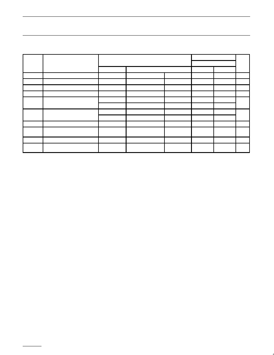
QUICK REFERENCE DATA
SYMBOL
PARAMETER
CONDITIONS
TYPICAL
UNIT
t
PLH
t
PHL
Propagation delay
BUF_IN to BUF_OUT
n
V
CC
= 3.3V, CL = 30pF
2.5
2.5
ns
t
r
Rise time
V
CC
= 3.3V, CL = 30pF
1.0
ns
t
f
Fall time
V
CC
= 3.3V, CL = 20pF
700
ps
I
CC
Total supply current
V
CC
= 3.465V
50
µ
A
ORDERING INFORMATION
PACKAGES
TEMPERATURE RANGE
ORDER CODE
DRAWING NUMBER
28-Pin Plastic SSOP
0
∞
C to +70
∞
C
PCK2001M DB
SOT341≠1
PIN CONFIGURATION
3
4
5
6
7
8
9
10
11
12
17
18
19
20
21
22
23
24
25
26
BUF_OUT1
V
SS0
V
DD1
BUF_OUT2
BUF_OUT3
V
SS1
BUF_IN
V
DD4
BUF_OUT16
BUF_OUT17
V
SS4
V
DD5
OE
V
SS8
BUF_OUT12
BUF_OUT13
V
DD8
V
SS9
BUF_OUT14
V
SS5
13
16
V
DDI2C
V
SSI2C
14
15
S
DA
S
CL
TOP VIEW
1
2
27
28
V
DD0
BUF_OUT0
BUF_OUT15
V
DD9
SA00447
PCK2001M
Intel and Pentium are registered trademarks of Intel Corporation.
I
2
C is a trademark of Philips Semiconductors Corporation.
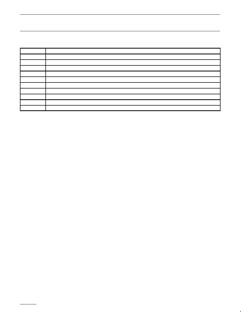
PIN DESCRIPTION
PIN
NUMBER
I/O
TYPE
SYMBOL
FUNCTION
2, 3, 6, 7
Output
BUF_OUT
(0≠3)
Buffered clock outputs
22, 23, 26, 27
Output
BUF_OUT
(12≠15)
Buffered clock outputs
11, 18
Output
BUF_OUT
(16≠17)
Buffered clock outputs
9
Input
BUF_IN
Buffered clock input
20
Input
OE
Active high ouput enable
14
I/O
SDA
I
2
C serial data
15
Input
SCL
I
2
C serial clock
1, 5, 10, 19,
24, 28
Input
V
DD (0≠9)
3.3V power supply
4, 8, 12, 17,
21, 25
Input
V
SS (0≠9)
Ground
13
Input
V
DDI2C
3.3V I
2
C power supply
16
Input
V
DDI2C
I
2
C ground

Philips Semiconductors
Product specification
PCK2001M
14.318≠150 MHz I
2
C 1:10 Clock Buffer
1999 Jul 06
3
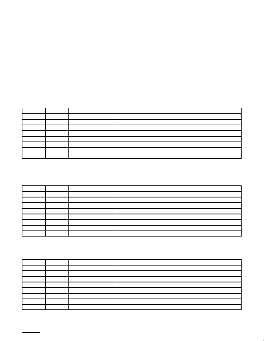
FUNCTION TABLE
OE
BUF_IN
I
2
CEN
BUF_OUTn
L
X
X
Z
H
L
X
L
H
H
H
H
H
H
L
L
ABSOLUTE MAXIMUM RATINGS
1, 2
In accordance with the Absolute Maximum Rating System (IEC 134)
Voltages are referenced to V
SS
(V
SS
= 0V)
SYMBOL
PARAMETER
CONDITION
LIMITS
UNIT
SYMBOL
PARAMETER
CONDITION
MIN
MAX
UNIT
V
DD
DC 3.3V supply voltage
≠0.5
+4.6
V
I
IK
DC input diode current
V
I
< 0
≠50
mA
V
I
DC input voltage
Note 2
≠0.5
5.5
V
I
OK
DC output diode current
V
O
> V
DD
or V
O
< 0
±
50
mA
V
O
DC output voltage
Note 2
≠0.5
V
CC
+ 0.5
V
I
O
DC output source or sink current
V
O
>= 0 to V
DD
±
50
mA
T
STG
Storage temperature range
≠65
+150
∞
C
P
TOT
Power dissipation per package
plastic medium-shrink SO (SSOP)
For temperature range: 0 to +70
∞
C
above +55
∞
C derate linearly with 11.3mW/K
850
mW
NOTES:
1. Stresses beyond those listed may cause permanent damage to the device. These are stress ratings only and functional operation of the
device at these or any other conditions beyond those indicated under "recommended operating conditions" is not implied. Exposure to
absolute-maximum-rated conditions for extended periods may affect device reliability.
2. The input and output voltage ratings may be exceeded if the input and output current ratings are observed.
RECOMMENDED OPERATING CONDITIONS
SYMBOL
PARAMETER
CONDITIONS
LIMITS
UNIT
SYMBOL
PARAMETER
CONDITIONS
MIN
MAX
UNIT
V
DD
DC 3.3V supply voltage
3.135
3.465
V
C
L
Capacitive load
20
30
pF
V
I
DC input voltage range
0
V
DD
V
V
O
DC output voltage range
0
V
DD
V
T
amb
Operating ambient temperature range in free air
0
+70
∞
C
Philips Semiconductors
Product specification
PCK2001M
14.318≠150 MHz I
2
C 1:10 Clock Buffer
1999 Jul 06
4
DC CHARACTERISTICS
TEST CONDITIONS
LIMITS
SYMBOL
PARAMETER
TEST CONDITIONS
T
amb
= 0
∞
C to +70
∞
C
UNIT
V
DD
(V)
OTHER
MIN
MAX
V
IH
HIGH level input voltage
3.135 to 3.465
2.0
V
DD
+ 0.3
V
V
IL
LOW level input voltage
3.135 to 3.465
V
SS
≠ 0.3
0.8
V
V
OH
3.3V output HIGH voltage
3.135 to 3.465
I
OH
= ≠1mA
2.4
≠
V
V
OL
3.3V output LOW voltage
3.135 to 3.465
I
OL
= 1mA
≠
0.4
V
I
O
Output HIGH current
3.135 to 3.465
V
OUT
= 2.0V
≠54
≠
mA
I
OH
Output HIGH current
3.135 to 3.465
V
OUT
= 3.135V
≠
≠46
mA
I
O
Output LOW current
3.135 to 3.465
V
OUT
= 1.0V
54
≠
mA
I
OL
Output LOW current
3.135 to 3.465
V
OUT
= 0.4V
≠
53
mA
±
I
I
Input leakage current
3.465
≠
5
µ
A
±
I
OZ
3-State output OFF-State
current
3.465
V
OUT
= V
DD
or GND
I
O
= 0
≠
10
µ
A
I
CC
Quiescent supply current
3.465
V
I
= V
DD
or GND
I
O
= 0
≠
100
µ
A
I
CC
Additional quiescent supply
current given per control pin
3.135 to 3.465
V
I
= V
DD
≠ 0.6V
I
O
= 0
≠
500
µ
A

Philips Semiconductors
Product specification
PCK2001M
14.318≠150 MHz I
2
C 1:10 Clock Buffer
1999 Jul 06
5
SDRAM CLOCK OUTPUT BUFFER PULL-UP CHARACTERISTICS
PULL-UP
VOLTAGE
(V)
I
(mA)
(V)
MIN
TYP
MAX
0
≠72
≠116
≠198
1
≠72
≠116
≠198
1.40
≠68
≠110
≠188
1.50
≠67
≠107
≠184
1.65
≠64
≠103
≠177
1.80
≠60
≠98
≠170
2.00
≠54
≠90
≠157
2.40
≠39
≠69
≠126
2.60
≠30
≠56
≠107
3.135
0
≠15
≠46
3.30
0
≠23
3.465
0
SDRAM PULL-UP
SW00249
≠200
≠180
≠160
≠140
≠120
≠100
≠80
≠60
≠40
≠20
0
0
0.25
0.5 0.75
1
1.25
1.5 1.75
2
2.25
2.5 2.75
3
3.25
3.5
MIN
TYP
MAX
V
OUT
(V)
I
OH
(mA)

Philips Semiconductors
Product specification
PCK2001M
14.318≠150 MHz I
2
C 1:10 Clock Buffer
1999 Jul 06
6
SDRAM CLOCK OUTPUT BUFFER PULL-DOWN CHARACTERISTICS
PULL-UP
VOLTAGE
(V)
I
(mA)
(V)
MIN
TYP
MAX
0
0
0
0
0.4
23
34
53
0.65
35
52
83
0.85
43
65
104
1.00
49
74
118
1.4
61
93
152
1.5
64
98
159
1.65
67
103
168
1.8
70
108
177
1.95
72
112
184
3.135
72
112
204
3.6
112
204
SDRAM PULL-DOWN
0
25
50
75
100
125
150
175
200
225
0
0.4
0.8
1.2
1.6
2
2.4
2.8
3.2
3.6
MIN
TYP
MAX
V
OUT
(V)
I
OL
(mA)
SW00250

Philips Semiconductors
Product specification
PCK2001M
14.318≠150 MHz I
2
C 1:10 Clock Buffer
1999 Jul 06
7
AC CHARACTERISTICS
SYMBOL
PARAMETER
TEST CONDITIONS
LIMITS
T
amb
= 0
∞
C to +70
∞
C
UNIT
NOTES
MIN
TYP
9
MAX
T
SDKP
SDRAM CLK period
1, 6
15.0
15.2
15.5
T
SDKH
SDRAM CLK HIGH time
66MHz
2, 6, 8
5.6
7.8
8.4
ns
T
SDKL
SDRAM CLK LOW time
3, 6, 8
5.3
7.4
8.0
T
SDKP
SDRAM CLK period
1, 6
10.0
10.01
10.5
T
SDKH
SDRAM CLK HIGH time
100MHz
2, 6, 8
3.3
5.1
5.7
ns
T
SDKL
SDRAM CLK LOW time
3, 6, 8
3.1
4.9
5.5
T
SDKP
SDRAM CLK period
1, 6
7.4
7.5
7.7
T
SDKH
SDRAM CLK HIGH time
133MHz
2, 6, 8
2.6
3.2
3.8
ns
T
SDKL
SDRAM CLK LOW time
3, 6, 8
2.1
2.8
3.5
T
SDRISE
SDRAM rise time
4, 6, 10
1.5
2.0
4.0
V/ns
T
SDFALL
SDRAM fall time
4, 6, 11
1.5
2.9
4.0
V/ns
T
PLH
SDRAM buffer LH propagation delay
6, 7
1.0
2.5
3.5
ns
T
PHL
SDRAM buffer HL propagation delay
6, 7
1.0
2.5
3.5
ns
T
PZL
, T
PZH
SDRAM buffer enable time
6, 7
1.0
2.6
5.0
ns
T
PLZ
, T
PHZ
SDRAM buffer disable time
6, 7
1.0
2.7
5.0
ns
DUTY CYCLE
Output Duty Cycle
Measured at 1.5V
5, 6, 7
45
52
55
%
T
SDSKW
SDRAM Bus CLK skew
1, 6
150
250
ps
T
DDSKW
Device to device skew
250
ps
NOTES:
1. Clock period and skew are measured on the rising edge at 1.5V.
2. T
SDKH
is measured at 2.4V as shown in Figure 4.
3. T
SDKL
is measured at 0.4V as shown in Figure 4.
4. T
SDRISE
and T
SDFALL
are measured as a transition through the threshold region V
OL
= 0.4V and V
OH
= 2.4V (1mA) JEDEC specification.
5. Duty cycle should be tested with a 50/50% input.
6. Over MIN (20pF) to MAX (30pF) discrete load, process, voltage, and temperature.
7. Input edge rate for these tests must be faster than 1 V/ns.
8. Calculated at minimum edge rate (1.5ns) to guarantee 45/55% duty cycle at 1.5V. Pulsewidth is required to be wider at the faster edge to
ensure duty cycle specification is met.
9. All typical values are at V
CC
= 3.3V and T
amb
= 25
∞
C.
10. Typical is measured with MAX (30pf) discrete load.
11. Typical is measured with MIN (20pf) discrete load.

Philips Semiconductors
Product specification
PCK2001M
14.318≠150 MHz I
2
C 1:10 Clock Buffer
1999 Jul 06
8
I
2
C CONSIDERATIONS
I
2
C has been chosen as the serial bus interface to control the PCK2001M. I
2
C was chosen to support the JEDEC proposal JC-42.5 168 Pin
Unbuffered SDRAM DIMM. All vendors are required to determine the legal issues associated with the manufacture of I
2
C devices.
1) Address assignment: The clock driver in this specification uses the single, 7-bit address shown below. All devices can use the address if only
one master clock driver is used in a design. The address can be re-used for the CKBF device if no other conflicting I
2
C clock driver is used in
the system.
The following address was confirmed by Philips on 09/04/96.
A6
A5
A4
A3
A2
A1
A0
R/W#
1
1
0
1
0
0
1
0
NOTE: The R/W# bit is used by the I
2
C controller as a data direction bit. A `zero' indicates a transmission (WRITE) to the clock device. A `one'
indicates a request for data (READ) from the clock driver. Since the definition of the clock buffer only allows the controller to WRITE data; the
R/W# bit of the address will always be seen as `zero'. Optimal address decoding of this bit is left to the vendor.
2) Options: It is our understanding that metal mask options and other pinouts of this type of clock driver will be allowed to use the same address
as the original CKBF device. I
2
C addresses are defined in terms of function (master clock driver) rather than form (pinout, and option).
3) Slave/Receiver: The clock driver is assumed to require only slave/receiver functionality. Slave/transmitter functionality is optional.
4) Data Transfer Rate: 100 kbits/s (standard mode) is the base functionality required. Fast mode (400 kbits/s) functionality is optional.
5) Logic Levels: I
2
C logic levels are based on a percentage of V
DD
for the controller and other devices on the bus. Assume all devices are
based on a 3.3 Volt supply.
6) Data Byte Format: Byte format is 8 Bits as described in the following appendices.
7) Data Protocol: To simplify the clock I
2
C interface, the clock driver serial protocol was specified to use only block writes from the controller.
The bytes must be accessed in sequential order from lowest to highest byte with the ability to stop after any complete byte has been
transferred. Indexed bytes are not allowed. However, the SMBus controller has a more specific format than the generic I
2
C protocol.
The clock driver must meet this protocol which is more rigorous than previously stated I
2
C protocol. Treat the description from the viewpoint of
controller. The controller ``writes" to the clock driver and if possible would ``read" from the clock driver (the clock driver is a slave/receiver only
and is incapable of this transaction.)
``The block write begins with a slave address and a write condition. After the command code the host (controller) issues a byte count which
describes how many more bytes will follow in the message. If the host had 20 bytes to send, the first byte would be the number 20 (14h),
followed by the 20 bytes of data. The byte count may not be 0. A block write command is allowed to transfer a maximum of 32 data bytes."
SW00279
1 bit
7 bits
1
1
8 bits
1
Start bit
Slave Address
R/W
Command Code
Byte Count = N
Ack
Data Byte 1
Ack
Data Byte 2
Ack
...
Data Byte 2
Ack
Stop
Ack
Ack
1 bit
8 bits
1
1
8 bits
1
8 bits
1
NOTE: The acknowledgement bit is returned by the slave/receiver (the clock driver).
Consider the command code and the byte count bytes required as the first two bytes of any transfer. The command code is software
programmable via the controller, but will be specified as 0000 0000 in the clock specification. The byte count byte is the number of additional
bytes required to transfer, not counting the command code and byte count bytes. Additionally, the byte count byte is required to be a minimum of
1 byte and a maximum of 32 bytes to satisfy the above requirement.
Philips Semiconductors
Product specification
PCK2001M
14.318≠150 MHz I
2
C 1:10 Clock Buffer
1999 Jul 06
9
For example:
Byte count byte
Notes:
MSB
LSB
0000
0000
Not allowed. Must have at least one byte.
0000
0001
Data for functional and frequency select register (currently byte 0 in spec)
0000
0010
Reads first two bytes of data. (byte 0 then byte 1)
0000
0011
Reads first three bytes (byte 0, 1, 2 in order)
0000
0100
Reads first four bytes (byte 0, 1, 2, 3 in order)
0000
0101
Reads first five bytes (byte 0, 1, 2, 3, 4 in order)
0000
0110
Reads first six bytes (byte 0, 1, 2, 3, 4, 5 in order)
0000
0111
Reads first seven bytes (byte 0, 1, 2, 3, 4, 5, 6 in order)
0010
0000
Max byte count supported = 32
A transfer is considered valid after the acknowledge bit corresponding to the byte count is read by the controller. The serial controller interface
can be simplified by discarding the information in both the command code and the byte count bytes and simply reading all the bytes that are
sent to the clock driver after being addressed by the controller. It is expected that the controller will not provide more bytes than the clock driver
can handle. A clock vendor may choose to discard any number of bytes that exceed the defined byte count.
8) Clock stretching: The clock device must not hold/stretch the SCLOCK or SDATA lines low for more than 10 mS. Clock stretching is
discouraged and should only be used as a last resort. Stretching the clock/data lines for longer than this time puts the device in an error/time-out
mode and may not be supported in all platforms. It is assumed that all data transfers can be completed as specified without the use of
clock/data stretching.
9) General Call: It is assumed that the clock driver will not have to respond to the ``general call."
10) Electrical Characteristics: All electrical characteristics must meet the standard mode specifications found in section 15 of the I
2
C
specification.
a) Pull-Up Resistors: Any internal resistors pull-ups on the SDATA and SCLOCK inputs must be stated in the individual datasheet. The use of
internal pull-ups on these pins of below 100K is discouraged. Assume that the board designer will use a single external pull-up resistor for each
line and that these values are in the 5 - 6K Ohm range. Assume one I
2
C device per DIMM (serial presence detect), one I
2
C controller, one clock
driver plus one/two more I
2
C devices on the platform for capacitive loading purposes.
(b) Input Glitch Filters: Only fast mode I
2
C devices require input glitch filters to suppress bus noise. The clock driver is specified as a standard
mode device and is not required to support this feature.
11) PWR DWN#: If a clock driver is placed in PWR DWN# mode, the SDATA and SCLK inputs must be Tri-Stated and the device must retain all
programming information. I
dd
current due to the I
2
C circuitry must be characterized and in the data sheet.
For specific I
2
C information consult the Philips I
2
C Peripherals Data Handbook IC12 (1997)
Philips Semiconductors
Product specification
PCK2001M
14.318≠150 MHz I
2
C 1:10 Clock Buffer
1999 Jul 06
10
SERIAL CONFIGURATION MAP
The serial bits will be read by the clock buffer in the following order:
Byte 0 ≠ Bits 7, 6, 5, 4, 3, 2, 1, 0
Byte 1 ≠ Bits 7, 6, 5, 4, 3, 2, 1, 0
Byte 2 ≠ Bits 7, 6, 5, 4, 3, 2, 1, 0
All unused register bits (Reserved and N/A) should be desined as "Dont Care". It is expected that the controller will force all of these bits to a "0"
level.
All register bits labeled "Initialize to 0" must be written to zero during intialization. Failure to do so may result in a higher than normal operating
current. The controller will read back the last written value.
Byte 0:
Output active/inactive register
1 = enable; 0 = disable
BIT
PIN#
NAME
DESCRIPTION
7
--
BUF_OUT7
Initialize to 0
6
--
BUF_OUT6
Initialize to 0
5
--
BUF_OUT5
Initialize to 0
4
--
BUF_OUT4
Initialize to 0
3
7
BUF_OUT3
Active/Inactive
2
6
BUF_OUT2
Active/Inactive
1
3
BUF_OUT1
Active/Inactive
0
2
BUF_OUT0
Active/Inactive
NOTE:
1. Inactive means outputs are held LOW and are disabled from switching. These outputs are designed to be configured at power-on and are
not expected to be configured during the normal modes of operation.
Byte 1:
Output active/inactive register
1 = enable; 0 = disable
BIT
PIN#
NAME
DESCRIPTION
7
27
BUF_OUT15
Active/Inactive
6
26
BUF_OUT14
Active/Inactive
5
23
BUF_OUT13
Active/Inactive
4
22
BUF_OUT12
Active/Inactive
3
--
BUF_OUT11
Initialize to 0
2
--
BUF_OUT10
Initialize to 0
1
--
BUF_OUT9
Initialize to 0
0
--
BUF_OUT8
Initialize to 0
NOTE:
1. Inactive means outputs are held LOW and are disabled from switching. These outputs are designed to be configured at power-on and are
not expected to be configured during the normal modes of operation.
Byte 2:
Optional register for possible future requirments
BIT
PIN#
NAME
DESCRIPTION
7
18
BUF_OUT17
Active/Inactive
6
11
BUF_OUT16
Active/Inactive
5
--
(reserved)
(reserved)
4
--
(reserved)
(reserved)
3
--
(reserved)
(reserved)
2
--
(reserved)
(reserved)
1
--
(reserved)
(reserved)
0
--
(reserved)
(reserved)
NOTE:
1. Inactive means outputs are held LOW and are disabled from switching. These outputs are designed to be configured at power-on and are
not expected to be configured during the normal modes of operation.

Philips Semiconductors
Product specification
PCK2001M
14.318≠150 MHz I
2
C 1:10 Clock Buffer
1999 Jul 06
11
AC WAVEFORMS
V
M
= 1.5V
V
X
= V
OL
+ 0.3V
V
Y
= V
OH
≠0.3V
V
OL
and V
OH
are the typical output voltage drop that occur with the
output load.
BUF_IN
INPUT
VM
tPLH
tPHL
BUF_OUT
VM
VM
VM
SW00246
V
DD
Figure 1. Load circuitry for switching times.
t
PLZ
t
PZL
V
I
nOE INPUT
GND
V
DD
OUTPUT
LOW-to-OFF
OFF-to-LOW
V
OL
V
OH
OUTPUT
HIGH-to-OFF
OFF-to-HIGH
V
SS
outputs
enabled
outputs
enabled
outputs
disabled
t
PHZ
V
M
V
M
V
M
t
PZH
V
X
V
Y
SW00245
V
DD
Figure 2. 3-State enable and disable times
DUTY CYCLE
T
SDKP
T
SDKH
T
SDRISE
T
SDFALL
T
SDKL
2.4
1.5
0.4
SW00247
Figure 3. SDRAM Output clock
DUTY CYCLE
t
kp
t
kh
t
r
t
f
t
kl
2.4
1.5
0.4
SW00479
Figure 4. Buffer Output clock
TEST CIRCUIT
PULSE
GENERATOR
RT
VI
D.U.T.
VO
C
L
VDD
TEST
S
1
t
PLH
/t
PHL
Open
t
PLZ
/t
PZL
2
<
V
DD
t
PHZ
/t
PZH
V
SS
Open
V
SS
S
1
2
<
V
DD
500
500
SW00251
Figure 5. Load circuitry for switching times

14.318-150 MHz I
2
C 1:10 Clock Buffer
Philips Semiconductors
Product specification
PCK2001M
1999 Jul 06
12
SSOP28:
plastic shrink small outline package; 28 leads; body width 5.3mm
SOT341-1

14.318-150 MHz I
2
C 1:10 Clock Buffer
Philips Semiconductors
Product specification
PCK2001M
1999 Jul 06
13
Definitions
Short-form specification -- The data in a short-form specification is extracted from a full data sheet with the same type number and title. For
detailed information see the relevant data sheet or data handbook.
Limiting values definition -- Limiting values given are in accordance with the Absolute Maximum Rating System (IEC 134). Stress above one
or more of the limiting values may cause permanent damage to the device. These are stress ratings only and operation of the device at these or
at any other conditions above those given in the Characteristics sections of the specification is not implied. Exposure to limiting values for extended
periods may affect device reliability.
Application information -- Applications that are described herein for any of these products are for illustrative purposes only. Philips
Semiconductors make no representation or warranty that such applications will be suitable for the specified use without further testing or
modification.
Disclaimers
Life support -- These products are not designed for use in life support appliances, devices or systems where malfunction of these products can
reasonably be expected to result in personal injury. Philips Semiconductors customers using or selling these products for use in such applications
do so at their own risk and agree to fully indemnify Philips Semiconductors for any damages resulting from such application.
Right to make changes -- Philips Semiconductors reserves the right to make changes, without notice, in the products, including circuits, standard
cells, and/or software, described or contained herein in order to improve design and/or performance. Philips Semiconductors assumes no
responsibility or liability for the use of any of these products, conveys no license or title under any patent, copyright, or mask work right to these
products, and makes no representations or warranties that these products are free from patent, copyright, or mask work right infringement, unless
otherwise specified.
Philips Semiconductors
811 East Arques Avenue
P.O. Box 3409
Sunnyvale, California 94088≠3409
Telephone 800-234-7381
©
Copyright Philips Electronics North America Corporation 1999
All rights reserved. Printed in U.S.A.
Date of release: 07-99
Document order number:
9397-750-06209
Philips
Semiconductors
Data sheet
status
Objective
specification
Preliminary
specification
Product
specification
Product
status
Development
Qualification
Production
Definition
[1]
This data sheet contains the design target or goal specifications for product development.
Specification may change in any manner without notice.
This data sheet contains preliminary data, and supplementary data will be published at a later date.
Philips Semiconductors reserves the right to make changes at any time without notice in order to
improve design and supply the best possible product.
This data sheet contains final specifications. Philips Semiconductors reserves the right to make
changes at any time without notice in order to improve design and supply the best possible product.
Data sheet status
[1]
Please consult the most recently issued datasheet before initiating or completing a design.