
DATA SHEET
Product specification
File under Discrete Semiconductors, SC07
April 1995
DISCRETE SEMICONDUCTORS
PMBF4391; PMBF4392;
PMBF4393
N-channel FETs

April 1995
2
Philips Semiconductors
Product specification
N-channel FETs
PMBF4391;
PMBF4392; PMBF4393
DESCRIPTION
Symmetrical silicon n-channel
depletion type junction field-effect
transistors on a plastic
microminiature envelope intended for
application in thick and thin-film
circuits. The transistors are intended
for low-power chopper or switching
applications in industry.
PINNING
Note
1. Drain and source are
interchangeable.
Marking code
1
= drain
2
= source
3
= gate
PMBF4391 = p6J
PMBF4392 = p6K
PMBF4393 = p6G
Fig.1 Simplified outline and symbol, SOT23.
handbook, halfpage
1
2
g
d
s
3
Top view
MAM385
QUICK REFERENCE DATA
PMBF4391
PMBF4392
PMBF4393
Drain-source voltage
�
V
DS
max.
40
40
40
V
Drain current
V
DS
= 20 V; V
GS
= 0
I
DSS
>
50
25
5
mA
Gate-source cut-off voltage
V
DS
= 20 V; I
D
= 1 nA
-
V
(P)GS
>
4
2
0.5
V
<
10
5
3
V
Drain-source resistance (on) at f = 1 kHz
I
D
= 0; V
GS
= 0
R
ds on
<
30
60
100
Feedback capacitance at f = 1 MHz
-
V
GS
= 12 V; V
DS
= 0
C
rs
<
3.5
3.5
3.5
pF
Turn-off time
V
DD
= 10 V; V
GS
= 0
I
D
= 12 mA;
-
V
GSM
= 12 V
t
off
<
20
-
-
ns
I
D
= 6 mA;
-
V
GSM
= 7 V
t
off
<
-
35
-
ns
I
D
= 3 mA;
-
V
GSM
= 5 V
t
off
<
-
-
50
ns

April 1995
3
Philips Semiconductors
Product specification
N-channel FETs
PMBF4391; PMBF4392;
PMBF4393
RATINGS
Limiting values in accordance with the Absolute Maximum System (IEC 134)
THERMAL RESISTANCE
CHARACTERISTICS
T
j
= 25
�
C unless otherwise specified
Drain-source voltage
�
V
DS
max.
40 V
Drain-gate voltage
V
DGO
max.
40 V
Gate-source voltage
-
V
GSO
max.
40 V
Gate current (DC)
I
G
max.
50 mA
Total power dissipation up to T
amb
= 40
�
C
(1)
P
tot
max.
250 mW
Storage temperature range
T
stg
-
65 to
+
150
�
C
Junction temperature
T
j
max.
150
�
C
From junction to ambient
(1)
R
th j-a
=
430 K/W
Gate-source voltage
I
G
= 1 mA; V
DS
= 0
V
GSon
<
1 V
Gate-source cut-off current
V
DS
= 0 V;
-
V
GS
= 20 V
-
I
GSS
<
0.1 nA
V
DS
= 0 V;
-
V
GS
= 20 V; T
amb
= 150
�
C
-
I
GSS
<
0.2
�
A
PMBF4391
PMBF4392
PMBF4393
Drain current
V
DS
= 20 V; V
GS
= 0
I
DSS
>
<
50
150
25
75
5
30
mA
mA
Gate-source breakdown voltage
-
I
G
= 1
�
A; V
DS
= 0
-
V
(BR)GSS
>
40
40
40 V
Gate-source cut-off voltage
I
D
= 1 nA; V
DS
= 20 V
-
V
(P)GS
>
<
4
10
2
5
0.5
3
V
V
Drain-source voltage (on)
I
D
= 12 mA; V
GS
= 0
V
DSon
<
0.4
-
-
V
I
D
= 6 mA; V
GS
= 0
V
DSon
<
0.4
-
V
I
D
= 3 mA; V
GS
= 0
V
DSon
<
-
-
0.4 V
Drain-source resistance (on)
I
D
= 0; V
GS
= 0; f = 1 kHz; T
amb
= 25
�
C
r
ds on
<
30
-
100
Drain cut-off current
-
V
GS
= 12 V
V
DS
= 20 V
I
DSX
<
0.1
-
-
nA
-
V
GS
= 7 V
I
DSX
<
-
0.1
-
nA
-
V
GS
= 5 V
I
DSX
<
-
-
0.1 nA
-
V
GS
= 12 V
V
DS
= 20 V; T
amb
= 150
�
C
I
DSX
<
0.2
-
- �
A
-
V
GS
= 7 V
I
DSX
<
-
0.2
- �
A
-
V
GS
= 5 V
I
DSX
<
-
-
0.2
�
A
April 1995
4
Philips Semiconductors
Product specification
N-channel FETs
PMBF4391; PMBF4392;
PMBF4393
Note
1. Mounted on a ceramic substrate of 8 mm
�
10 mm
�
0,7 mm.
y-parameters (common source)
V
DS
= 20 V; V
GS
= 0; f = 1 MHz; T
amb
= 25
�
C
PMBF4391
PMBF4392
PMBF4393
Input capacitance
C
is
<
14
14
14 pF
Feedback capacitance
-
V
GS
= 12 V
; V
DS
= 0
C
rs
<
3.5
-
-
pF
-
V
GS
= 7 V
; V
DS
= 0
C
rs
<
-
3.5
-
pF
-
V
GS
= 5 V
; V
DS
= 0
C
rs
<
-
-
3.5 pF
Switching times
V
DD
= 10 V
; V
DS
= 0
Conditions I
D
and
-
V
GSoff
I
D
=
12
6
3 mA
-
V
GS off
=
12
7
5 V
R
L
=
750
1550
3150
Rise time
t
r
<
5
5
5 ns
Turn on time
t
on
<
15
15
15 ns
Fall time
t
f
<
15
20
30 ns
Turn off time
t
off
<
20
35
50 ns
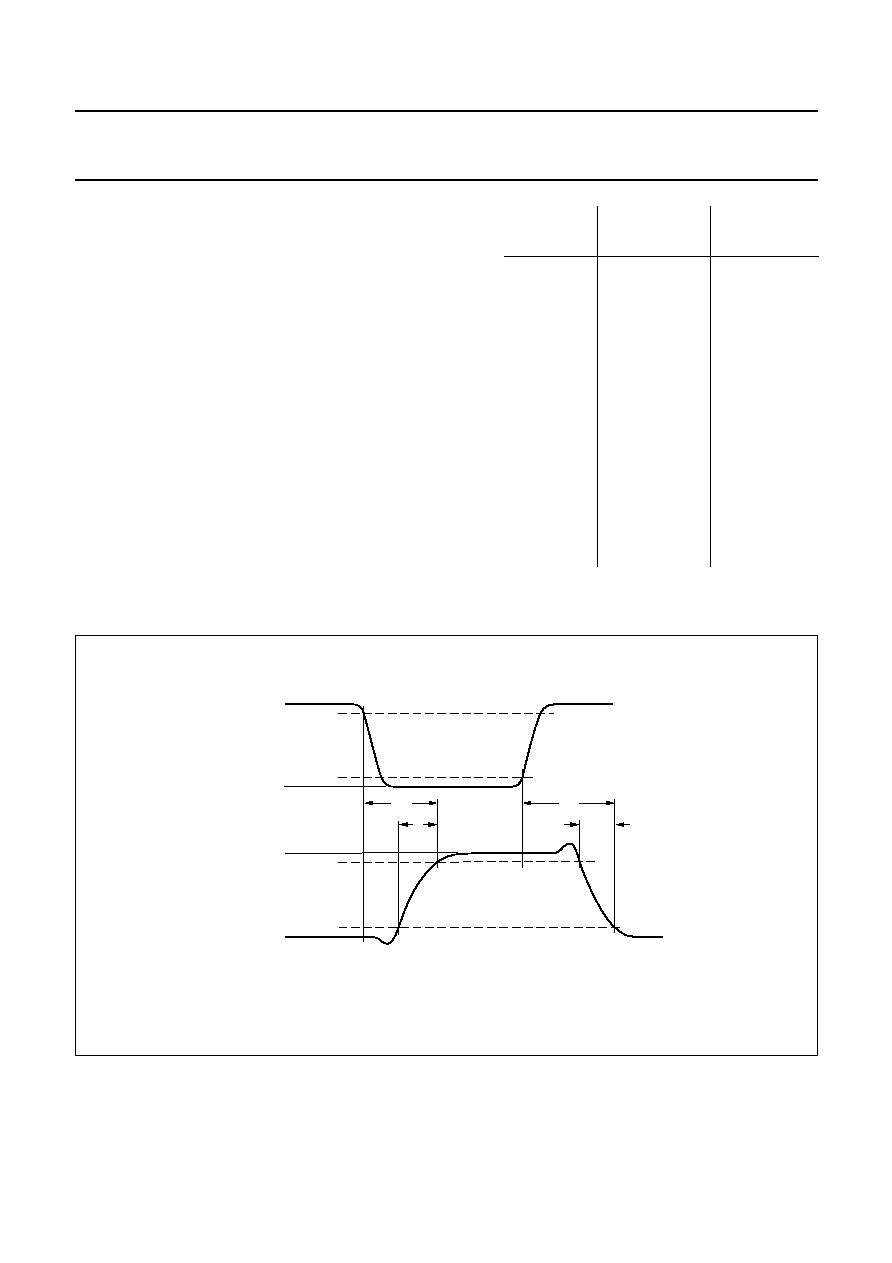
Fig.2 Switching times waveforms.
handbook, full pagewidth
MBK288
-
VGS off
toff
tf
VGS = 0 V
Vi
Vo
10%
90%
90%
10%
ton
tr

April 1995
5
Philips Semiconductors
Product specification
N-channel FETs
PMBF4391; PMBF4392;
PMBF4393
Fig.3 Test circuit.
handbook, halfpage
MBK289
50
RL
DUT
10
�
F
1
�
F
VDD
10 nF
50
SAMPLING
SCOPE
50
Pulse generator:
t
r
<
0.5 ns
t
f
<
0.5 ns
t
p
=
100
�
s
=
0.01
Oscilloscope:
R
i
=
50
Fig.4 Power derating curve.
handbook, halfpage
0
Tamb (
�
C)
Ptot
(mW)
300
200
100
0
40
200
80
120
160
MDA245
April 1995
6
Philips Semiconductors
Product specification
N-channel FETs
PMBF4391; PMBF4392;
PMBF4393
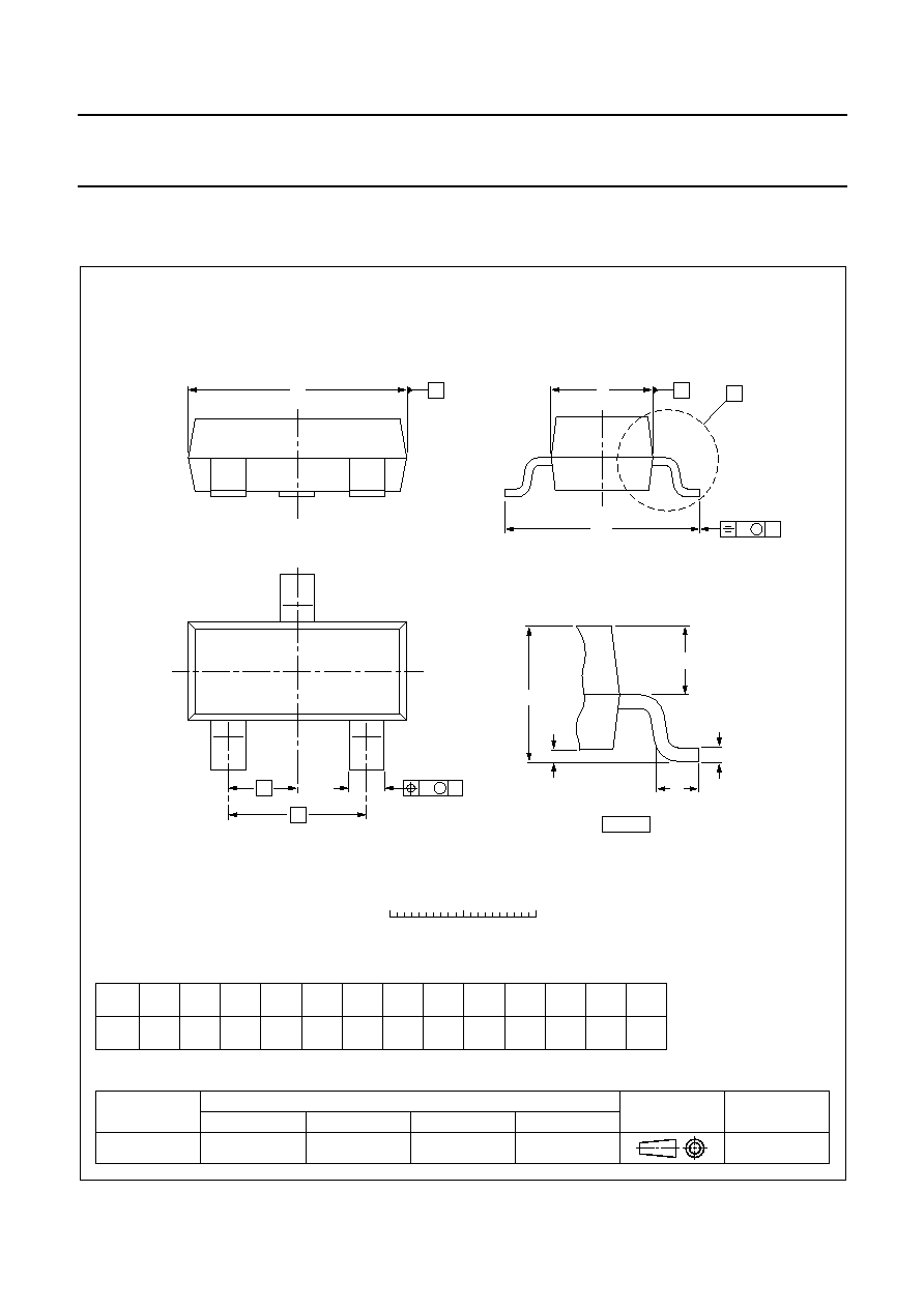
PACKAGE OUTLINE
UNIT
A
1
max.
b
p
c
D
E
e
1
H
E
L
p
Q
w
v
REFERENCES
OUTLINE
VERSION
EUROPEAN
PROJECTION
ISSUE DATE
97-02-28
IEC
JEDEC
EIAJ
mm
0.1
0.48
0.38
0.15
0.09
3.0
2.8
1.4
1.2
0.95
e
1.9
2.5
2.1
0.55
0.45
0.1
0.2
DIMENSIONS (mm are the original dimensions)
0.45
0.15
SOT23
bp
D
e1
e
A
A1
Lp
Q
detail X
HE
E
w
M
v
M
A
B
A
B
0
1
2 mm
scale
A
1.1
0.9
c
X
1
2
3
Plastic surface mounted package; 3 leads
SOT23

April 1995
7
Philips Semiconductors
Product specification
N-channel FETs
PMBF4391; PMBF4392;
PMBF4393
DEFINITIONS
LIFE SUPPORT APPLICATIONS
These products are not designed for use in life support appliances, devices, or systems where malfunction of these
products can reasonably be expected to result in personal injury. Philips customers using or selling these products for
use in such applications do so at their own risk and agree to fully indemnify Philips for any damages resulting from such
improper use or sale.
Data sheet status
Objective specification
This data sheet contains target or goal specifications for product development.
Preliminary specification
This data sheet contains preliminary data; supplementary data may be published later.
Product specification
This data sheet contains final product specifications.
Short-form specification
The data in this specification is extracted from a full data sheet with the same type
number and title. For detailed information see the relevant data sheet or data handbook.
Limiting values
Limiting values given are in accordance with the Absolute Maximum Rating System (IEC 134). Stress above one or
more of the limiting values may cause permanent damage to the device. These are stress ratings only and operation
of the device at these or at any other conditions above those given in the Characteristics sections of the specification
is not implied. Exposure to limiting values for extended periods may affect device reliability.
Application information
Where application information is given, it is advisory and does not form part of the specification.