Document Outline
- FEATURES
- APPLICATIONS
- GENERAL DESCRIPTION
- PINNING
- LIMITING VALUES
- ELECTRICAL CHARACTERISTICS
- THERMAL CHARACTERISTICS
- GRAPHICAL DATA
- PACKAGE OUTLINE
- DATA SHEET STATUS
- DEFINITIONS
- DISCLAIMERS

DATA SHEET
Product specification
2003 Jun 27
DISCRETE SEMICONDUCTORS
PMEG6010AED
Low V
F
(MEGA) Schottky barrier
diode
age
M3D302

2003 Jun 27
2
Philips Semiconductors
Product specification
Low V
F
(MEGA) Schottky barrier diode
PMEG6010AED
FEATURES
∑
Low switching losses
∑
Very high surge current absorption capability
∑
Fast recovery time
∑
Guard ring protected
∑
Plastic SMD package.
APPLICATIONS
∑
Low power switched-mode power supplies
∑
Rectification
∑
Polarity protection.
GENERAL DESCRIPTION
Planar Schottky barrier diode encapsulated in a SOT457
(SC-74) small plastic package.
PINNING
PIN
DESCRIPTION
1
cathode
2
cathode
3
anode
4
anode
5
cathode
6
cathode
handbook, halfpage
MHC634
1
3
2
4
5
6
1, 2
5, 6
3, 4
Fig.1
Simplified outline SOT457 (SC-74) and
symbol.
Marking code: M4.
LIMITING VALUES
In accordance with Absolute Maximum Rating System (IEC 60134).
Note
1. Device mounted on a printed-circuit board, single sided copper, tinplated, mounting pad for cathode 6 cm
2
.
SYMBOL
PARAMETER
CONDITIONS
MIN.
MAX.
UNIT
V
R
continuous reverse voltage
-
60
V
I
F
continuous forward current
T
amb
25
∞
C; note 1
-
1
A
I
FSM
non-repetitive peak forward current t = 8 ms; square wave
-
17.5
A
I
RSM
non-repetitive peak reverse current t
p
= 100
µ
s
-
0.5
A
T
stg
storage temperature
-
65
+150
∞
C
T
j
junction temperature
-
+150
∞
C

2003 Jun 27
3
Philips Semiconductors
Product specification
Low V
F
(MEGA) Schottky barrier diode
PMEG6010AED
ELECTRICAL CHARACTERISTICS
T
amb
= 25
∞
C; unless otherwise specified.
Notes
1. Pulse test: t
p
= 300
µ
s;
= 0.02.
2. For Schottky barrier diodes thermal runaway has to be considered, as in some applications, the reverse power losses
P
R
are a significant part of the total power losses.
THERMAL CHARACTERISTICS
Notes
1. Device mounted on a printed-circuit board, single-sided copper, tinplated, mounting pad for cathode 1 cm
2
.
2. Device mounted on a printed-circuit board, single-sided copper; tinplated, mounting pad for cathode 6 cm
2
.
SYMBOL
PARAMETER
CONDITIONS
MAX.
UNIT
V
F
continuous forward voltage
I
F
= 0.1 A
400
mV
I
F
= 1 A
650
mV
I
R
continuous reverse current
V
R
= 60 V; see Fig.3
350
µ
A
V
R
= 60 V; T
j
= 100
∞
C;
notes 1 and 2
8
mA
C
d
diode capacitance
V
R
= 4 V; f = 1 MHz; see Fig.4
60
pF
SYMBOL
PARAMETER
CONDITIONS
VALUE
UNIT
R
th j-a
thermal resistance from junction to ambient
in free air; note 1
230
K/W
in free air; note 2
180
K/W
2003 Jun 27
4
Philips Semiconductors
Product specification
Low V
F
(MEGA) Schottky barrier diode
PMEG6010AED
GRAPHICAL DATA
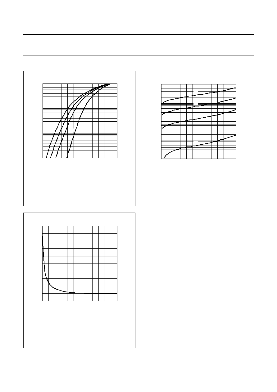
handbook, halfpage
0.6
0
0.2
0.4
10
3
10
2
10
1
MHC635
(1) (2) (3)
(4)
VF (V)
IF
(mA)
Fig.2
Forward current as a function of forward
voltage; typical values.
(1) T
amb
= 125
∞
C.
(2) T
amb
= 100
∞
C.
(3) T
amb
= 75
∞
C.
(4) T
amb
= 25
∞
C.
handbook, halfpage
60
20
0
40
10
-
2
10
-
3
10
-
4
10
-
5
10
-
6
MHC636
IR
(A)
VR (V)
(1)
(2)
(3)
(4)
Fig.3
Reverse current as a function of reverse
voltage; typical values.
(1) T
amb
= 125
∞
C.
(2) T
amb
= 100
∞
C.
(3) T
amb
= 75
∞
C.
(4) T
amb
= 25
∞
C.
handbook, halfpage
200
0
20
60
0
40
40
80
120
160
MHC637
Cd
(pF)
VR (V)
Fig.4
Diode capacitance as a function of reverse
voltage; typical values.
f = 1 MHz; T
amb
= 25
∞
C.
2003 Jun 27
5
Philips Semiconductors
Product specification
Low V
F
(MEGA) Schottky barrier diode
PMEG6010AED
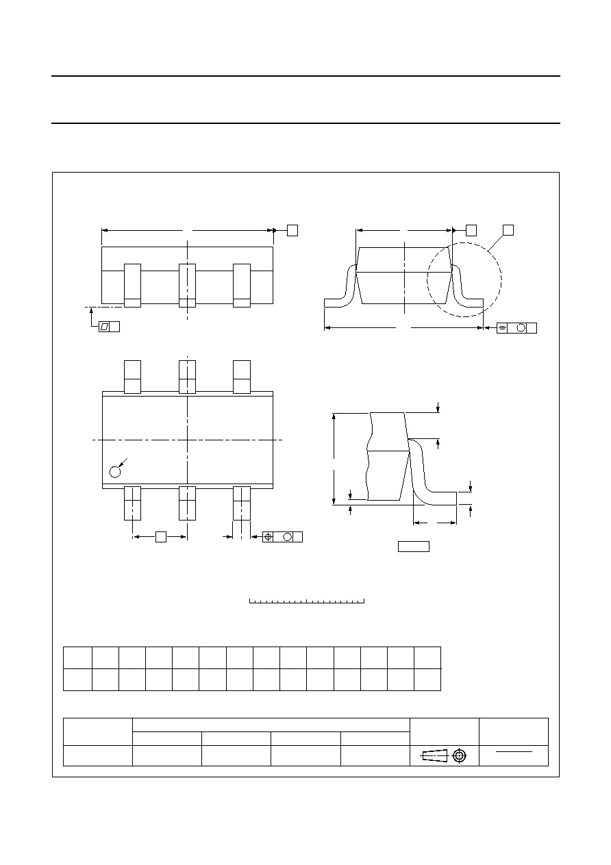
PACKAGE OUTLINE
REFERENCES
OUTLINE
VERSION
EUROPEAN
PROJECTION
ISSUE DATE
IEC
JEDEC
EIAJ
SOT457
SC-74
w
B
M
bp
D
e
pin 1
index
A
A1
Lp
Q
detail X
HE
E
v
M
A
A
B
y
0
1
2 mm
scale
c
X
1
3
2
4
5
6
Plastic surface mounted package; 6 leads
SOT457
UNIT
A1
bp
c
D
E
HE
Lp
Q
y
w
v
mm
0.1
0.013
0.40
0.25
3.1
2.7
0.26
0.10
1.7
1.3
e
0.95
3.0
2.5
0.2
0.1
0.2
DIMENSIONS (mm are the original dimensions)
0.6
0.2
0.33
0.23
A
1.1
0.9
97-02-28
01-05-04

2003 Jun 27
6
Philips Semiconductors
Product specification
Low V
F
(MEGA) Schottky barrier diode
PMEG6010AED
DATA SHEET STATUS
Notes
1. Please consult the most recently issued data sheet before initiating or completing a design.
2. The product status of the device(s) described in this data sheet may have changed since this data sheet was
published. The latest information is available on the Internet at URL http://www.semiconductors.philips.com.
3. For data sheets describing multiple type numbers, the highest-level product status determines the data sheet status.
LEVEL
DATA SHEET
STATUS
(1)
PRODUCT
STATUS
(2)(3)
DEFINITION
I
Objective data
Development
This data sheet contains data from the objective specification for product
development. Philips Semiconductors reserves the right to change the
specification in any manner without notice.
II
Preliminary data Qualification
This data sheet contains data from the preliminary specification.
Supplementary data will be published at a later date. Philips
Semiconductors reserves the right to change the specification without
notice, in order to improve the design and supply the best possible
product.
III
Product data
Production
This data sheet contains data from the product specification. Philips
Semiconductors reserves the right to make changes at any time in order
to improve the design, manufacturing and supply. Relevant changes will
be communicated via a Customer Product/Process Change Notification
(CPCN).
DEFINITIONS
Short-form specification
The data in a short-form
specification is extracted from a full data sheet with the
same type number and title. For detailed information see
the relevant data sheet or data handbook.
Limiting values definition
Limiting values given are in
accordance with the Absolute Maximum Rating System
(IEC 60134). Stress above one or more of the limiting
values may cause permanent damage to the device.
These are stress ratings only and operation of the device
at these or at any other conditions above those given in the
Characteristics sections of the specification is not implied.
Exposure to limiting values for extended periods may
affect device reliability.
Application information
Applications that are
described herein for any of these products are for
illustrative purposes only. Philips Semiconductors make
no representation or warranty that such applications will be
suitable for the specified use without further testing or
modification.
DISCLAIMERS
Life support applications
These products are not
designed for use in life support appliances, devices, or
systems where malfunction of these products can
reasonably be expected to result in personal injury. Philips
Semiconductors customers using or selling these products
for use in such applications do so at their own risk and
agree to fully indemnify Philips Semiconductors for any
damages resulting from such application.
Right to make changes
Philips Semiconductors
reserves the right to make changes in the products -
including circuits, standard cells, and/or software -
described or contained herein in order to improve design
and/or performance. When the product is in full production
(status `Production'), relevant changes will be
communicated via a Customer Product/Process Change
Notification (CPCN). Philips Semiconductors assumes no
responsibility or liability for the use of any of these
products, conveys no licence or title under any patent,
copyright, or mask work right to these products, and
makes no representations or warranties that these
products are free from patent, copyright, or mask work
right infringement, unless otherwise specified.

2003 Jun 27
7
Philips Semiconductors
Product specification
Low V
F
(MEGA) Schottky barrier diode
PMEG6010AED
NOTES

© Koninklijke Philips Electronics N.V. 2003
SCA75
All rights are reserved. Reproduction in whole or in part is prohibited without the prior written consent of the copyright owner.
The information presented in this document does not form part of any quotation or contract, is believed to be accurate and reliable and may be changed
without notice. No liability will be accepted by the publisher for any consequence of its use. Publication thereof does not convey nor imply any license
under patent- or other industrial or intellectual property rights.
Philips Semiconductors ≠ a worldwide company
Contact information
For additional information please visit http://www.semiconductors.philips.com.
Fax: +31 40 27 24825
For sales offices addresses send e-mail to: sales.addresses@www.semiconductors.philips.com.
Printed in The Netherlands
613514/01/pp
8
Date of release:
2003 Jun 27
Document order number:
9397 750 11455