Philips Semiconductors
Product specification
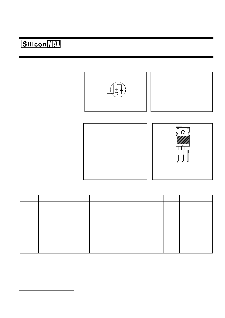
N-channel logic level TrenchMOS
TM
transistor
PSMN004-55W
FEATURES
SYMBOL
QUICK REFERENCE DATA
∑ 'Trench' technology
V
DSS
= 55 V
∑ Very low on-state resistance
∑ Fast switching
I
D
= 100 A
∑ Low thermal resistance
∑ Logic level compatible
R
DS(ON)
4.2 m
(V
GS
= 10 V)
R
DS(ON)
4.5 m
(V
GS
= 5 V)
R
DS(ON)
5 m
(V
GS
= 4.5 V)
GENERAL DESCRIPTION
PINNING
SOT429 (TO247)
SiliconMAX products use the latest
PIN
DESCRIPTION
Philips
Trench
technology
to
achieve
the
lowest
possible
1
gate
on-state
resistance
in
each
package at each voltage rating.
2
drain
Applications:-
3
source
∑ d.c. to d.c. converters
∑ switched mode power supplies
tab
drain
The PSMN004-55W is supplied in
the SOT429 (TO247) conventional
leaded package.
LIMITING VALUES
Limiting values in accordance with the Absolute Maximum System (IEC 134)
SYMBOL PARAMETER
CONDITIONS
MIN.
MAX.
UNIT
V
DSS
Drain-source voltage
T
j
= 25 ∞C to 175∞C
-
55
V
V
DGR
Drain-gate voltage
T
j
= 25 ∞C to 175∞C; R
GS
= 20 k
-
55
V
V
GS
Continuous gate-source
-
±
15
V
voltage
V
GSM
Peak pulsed gate-source
T
j
150 ∞C
-
±
20
V
voltage
I
D
Continuous drain current
T
mb
= 25 ∞C; V
GS
= 5 V
-
100
1
A
T
mb
= 100 ∞C; V
GS
= 5 V
-
100
1
A
I
DM
Pulsed drain current
T
mb
= 25 ∞C
-
300
A
P
D
Total power dissipation
T
mb
= 25 ∞C
-
300
W
T
j
, T
stg
Operating junction and
- 55
175
∞C
storage temperature
d
g
s
2
3
1
1 Maximum continuous current limited by package.
October 1999
1
Rev 1.100
Philips Semiconductors
Product specification
N-channel logic level TrenchMOS
TM
transistor
PSMN004-55W
AVALANCHE ENERGY LIMITING VALUES
Limiting values in accordance with the Absolute Maximum System (IEC 134)
SYMBOL PARAMETER
CONDITIONS
MIN.
MAX.
UNIT
E
AS
Non-repetitive avalanche
Unclamped inductive load, I
AS
= 100 A;
-
357
mJ
energy
t
p
= 100
µ
s; T
j
prior to avalanche = 25∞C;
V
DD
25 V; R
GS
= 50
; V
GS
= 5 V; refer to
fig:15
I
AS
Non-repetitive avalanche
-
100
A
current
THERMAL RESISTANCES
SYMBOL PARAMETER
CONDITIONS
MIN.
TYP. MAX. UNIT
R
th j-mb
Thermal resistance junction
-
-
0.5
K/W
to mounting base
R
th j-a
Thermal resistance junction
in free air
-
45
-
K/W
to ambient
ELECTRICAL CHARACTERISTICS
T
j
= 25∞C unless otherwise specified
SYMBOL PARAMETER
CONDITIONS
MIN.
TYP. MAX. UNIT
V
(BR)DSS
Drain-source breakdown
V
GS
= 0 V; I
D
= 0.25 mA;
55
-
-
V
voltage
T
j
= -55∞C
42
-
-
V
V
GS(TO)
Gate threshold voltage
V
DS
= V
GS
; I
D
= 1 mA
1
1.5
2
V
T
j
= 175∞C
0.5
-
-
V
T
j
= -55∞C
-
-
2.3
V
R
DS(ON)
Drain-source on-state
V
GS
= 10 V; I
D
= 25 A
-
3.2
4.2
m
resistance
V
GS
= 5 V; I
D
= 25 A
-
3.6
4.5
m
V
GS
= 4.5 V; I
D
= 25 A
-
3.8
5
m
V
GS
= 5 V; I
D
= 25 A; T
j
= 175∞C
-
6.2
9.5
m
I
GSS
Gate-source leakage current V
GS
=
±
10 V; V
DS
= 0 V;
-
0.02
100
nA
I
DSS
Zero gate voltage drain
V
DS
= 55 V; V
GS
= 0 V;
-
0.05
10
µ
A
current
T
j
= 175∞C
-
-
500
µ
A
Q
g(tot)
Total gate charge
I
D
= 100 A; V
DD
= 44 V; V
GS
= 5 V
-
226
-
nC
Q
gs
Gate-source charge
-
36
-
nC
Q
gd
Gate-drain (Miller) charge
-
106
-
nC
t
d on
Turn-on delay time
V
DD
= 30 V; R
D
= 1.2
;
-
26
-
ns
t
r
Turn-on rise time
V
GS
= 10 V; R
G
= 5.6
-
118
-
ns
t
d off
Turn-off delay time
Resistive load
-
848
-
ns
t
f
Turn-off fall time
-
336
-
ns
L
d
Internal drain inductance
Measured tab to centre of die
-
3.5
-
nH
L
d
Internal drain inductance
Measured from drain lead to centre of die
-
4.5
-
nH
L
s
Internal source inductance
Measured from source lead to source
-
7.5
-
nH
bond pad
C
iss
Input capacitance
V
GS
= 0 V; V
DS
= 25 V; f = 1 MHz
-
13
-
nF
C
oss
Output capacitance
-
1900
-
pF
C
rss
Feedback capacitance
-
1250
-
pF
October 1999
2
Rev 1.100
Philips Semiconductors
Product specification
N-channel logic level TrenchMOS
TM
transistor
PSMN004-55W
REVERSE DIODE LIMITING VALUES AND CHARACTERISTICS
T
j
= 25∞C unless otherwise specified
SYMBOL PARAMETER
CONDITIONS
MIN.
TYP. MAX. UNIT
I
S
Continuous source current
-
-
100
A
(body diode)
I
SM
Pulsed source current (body
-
-
300
A
diode)
V
SD
Diode forward voltage
I
F
= 25 A; V
GS
= 0 V
-
0.78
1.2
V
I
F
= 75 A; V
GS
= 0 V
-
0.92
-
t
rr
Reverse recovery time
I
F
= 20 A; -dI
F
/dt = 100 A/
µ
s;
-
150
-
ns
Q
rr
Reverse recovery charge
V
GS
= -10 V; V
R
= 20 V
-
0.7
-
µ
C
October 1999
3
Rev 1.100
Philips Semiconductors
Product specification
N-channel logic level TrenchMOS
TM
transistor
PSMN004-55W
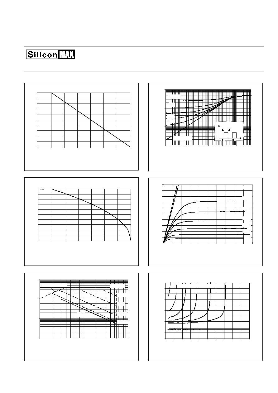
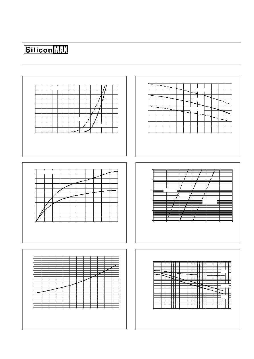
Fig.1. Normalised power dissipation.
PD% = 100
P
D
/P
D 25 ∞C
= f(T
mb
)
Fig.2. Normalised continuous drain current.
ID% = 100
I
D
/I
D 25 ∞C
= f(T
mb
); conditions: V
GS
5 V
Fig.3. Safe operating area. T
mb
= 25 ∞C
I
D
& I
DM
= f(V
DS
); I
DM
single pulse; parameter t
p
Fig.4. Transient thermal impedance.
Z
th j-mb
= f(t); parameter D = t
p
/T
Fig.5. Typical output characteristics, T
j
= 25 ∞C.
I
D
= f(V
DS
)
Fig.6. Typical on-state resistance, T
j
= 25 ∞C.
R
DS(ON)
= f(I
D
)
Normalised Power Derating, PD (%)
0
10
20
30
40
50
60
70
80
90
100
0
25
50
75
100
125
150
175
Mounting Base temperature, Tmb (C)
0.001
0.01
0.1
1
1E-06
1E-05
1E-04
1E-03
1E-02
1E-01
1E+00
Pulse width, tp (s)
Transient thermal impedance, Zth j-mb (K/W)
single pulse
D = 0.5
0.2
0.1
0.05
0.02
tp
D = tp/T
D
P
T
Normalised Current Derating, ID (%)
0
10
20
30
40
50
60
70
80
90
100
0
25
50
75
100
125
150
175
Mounting Base temperature, Tmb (C)
0
10
20
30
40
50
60
70
80
90
100
0
0.2
0.4
0.6
0.8
1
1.2
1.4
1.6
1.8
2
Drain-Source Voltage, VDS (V)
Drain Current, ID (A)
2.2 V
Tj = 25 C
VGS = 10V
2.3 V
2.4 V
2.5 V
2 V
10 V
2.1 V
1
10
100
1000
1
10
100
Drain-Source Voltage, VDS (V)
Peak Pulsed Drain Current, IDM (A)
D.C.
100 ms
10 ms
RDS(on) = VDS/ ID
1 ms
tp = 10 us
100 us
0
0.002
0.004
0.006
0.008
0.01
0.012
0.014
0.016
0.018
0.02
0
10
20
30
40
50
60
70
80
90
100
Drain Current, ID (A)
Drain-Source On Resistance, RDS(on) (Ohms)
VGS = 10V
Tj = 25 C
2.4 V
5 V
2.5 V
2.2 V
2.3 V
2 V
2.1 V
October 1999
4
Rev 1.100
Philips Semiconductors
Product specification
N-channel logic level TrenchMOS
TM
transistor
PSMN004-55W
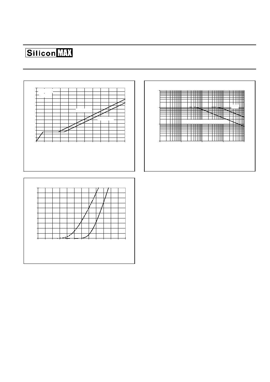
Fig.7. Typical transfer characteristics.
I
D
= f(V
GS
)
Fig.8. Typical transconductance, T
j
= 25 ∞C.
g
fs
= f(I
D
)
Fig.9. Normalised drain-source on-state resistance.
R
DS(ON)
/R
DS(ON)25 ∞C
= f(T
j
)
Fig.10. Gate threshold voltage.
V
GS(TO)
= f(T
j
); conditions: I
D
= 1 mA; V
DS
= V
GS
Fig.11. Sub-threshold drain current.
I
D
= f(V
GS)
; conditions: T
j
= 25 ∞C; V
DS
= V
GS
Fig.12. Typical capacitances, C
iss
, C
oss
, C
rss
.
C = f(V
DS
); conditions: V
GS
= 0 V; f = 1 MHz
0
10
20
30
40
50
60
70
80
90
100
0
0.2 0.4 0.6 0.8
1
1.2 1.4 1.6 1.8
2
2.2 2.4 2.6 2.8
3
Gate-source voltage, VGS (V)
Drain current, ID (A)
VDS > ID X RDS(ON)
Tj = 25 C
175 C
Threshold Voltage, VGS(TO) (V)
0
0.25
0.5
0.75
1
1.25
1.5
1.75
2
2.25
-60
-40
-20
0
20
40
60
80
100 120 140 160 180
Junction Temperature, Tj (C)
typical
maximum
minimum
0
20
40
60
80
100
120
140
160
180
200
220
0
10
20
30
40
50
60
70
80
90
100
Drain current, ID (A)
Transconductance, gfs (S)
Tj = 25 C
175 C
VDS > ID X RDS(ON)
Drain current, ID (A)
1.0E-06
1.0E-05
1.0E-04
1.0E-03
1.0E-02
1.0E-01
0
0.5
1
1.5
2
2.5
3
Gate-source voltage, VGS (V)
minimum
typical
maximum
Normalised On-state Resistance
0
0.2
0.4
0.6
0.8
1
1.2
1.4
1.6
1.8
2
2.2
2.4
-60
-40
-20
0
20
40
60
80
100 120 140 160 180
Junction temperature, Tj (C)
100
1000
10000
100000
0.1
1
10
100
Drain-Source Voltage, VDS (V)
Capacitances, Ciss, Coss, Crss (pF)
Ciss
Coss
Crss
October 1999
5
Rev 1.100
Philips Semiconductors
Product specification
N-channel logic level TrenchMOS
TM
transistor
PSMN004-55W
Fig.13. Typical turn-on gate-charge characteristics.
V
GS
= f(Q
G
)
Fig.14. Typical reverse diode current.
I
F
= f(V
SDS
); conditions: V
GS
= 0 V; parameter T
j
Fig.15. Maximum permissible non-repetitive
avalanche current (I
AS
) versus avalanche time (t
AV
);
unclamped inductive load
0
1
2
3
4
5
6
7
8
9
10
11
12
13
14
15
0
40
80
120
160
200
240
280
320
360
400
440
Gate charge, QG (nC)
Gate-source voltage, VGS (V)
ID = 100 A
Tj = 25 C
VDD = 11 V
VDD = 44 V
1
10
100
1000
0.001
0.01
0.1
1
10
Avalanche time, t
AV
(ms)
Maximum Avalanche Current, I
AS
(A)
Tj prior to avalanche = 150 C
25 C
0
10
20
30
40
50
60
70
80
90
100
0
0.1
0.2
0.3
0.4
0.5
0.6
0.7
0.8
0.9
1
1.1
1.2
Source-Drain Voltage, VSDS (V)
Source-Drain Diode Current, IF (A)
Tj = 25 C
175 C
VGS = 0 V
October 1999
6
Rev 1.100
Philips Semiconductors
Product specification
N-channel logic level TrenchMOS
TM
transistor
PSMN004-55W
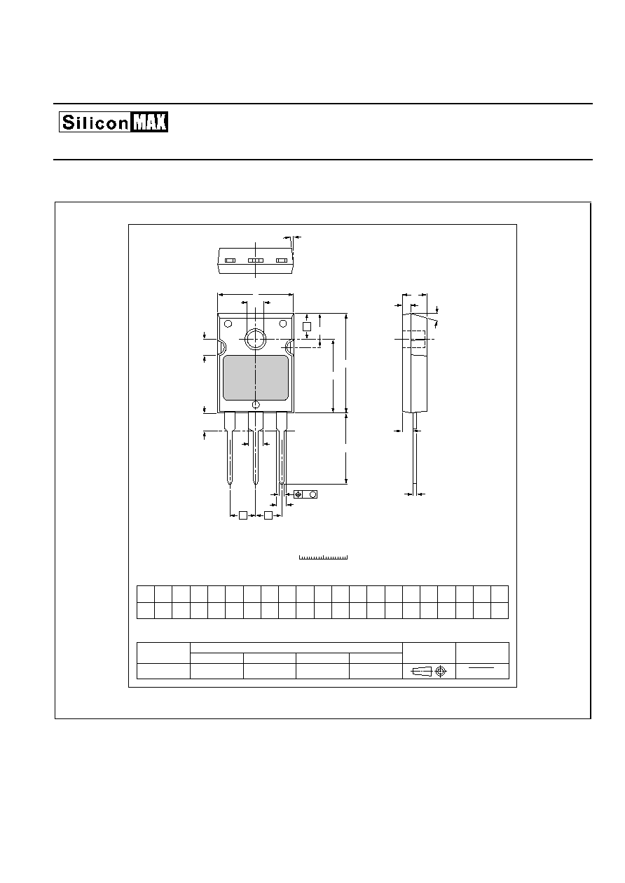
MECHANICAL DATA
Fig.16. SOT429; pin 2 connected to mounting base
Notes
1. Observe the general handling precautions for electrostatic-discharge sensitive devices (ESDs) to prevent
damage to MOS gate oxide.
2. Refer to mounting instructions for SOT429 envelope.
3. Epoxy meets UL94 V0 at 1/8".
REFERENCES
OUTLINE
VERSION
EUROPEAN
PROJECTION
ISSUE DATE
IEC
JEDEC
EIAJ
SOT429
TO-247
98-04-07
99-08-04
0
10
20 mm
scale
Plastic single-ended through-hole package; heatsink mounted; 1 mounting hole; 3-lead TO-247
SOT429
E
P
A
A1
w
M
b
1
2
3
e
e
b1
b2
c
Q
q
L
Y
R
D
S
L1
(1)
UNIT
A1
D
b
E
e
w
S
R
q
Q
P
L
Y
b2
b1
c
L1
(1)
DIMENSIONS (mm are the original dimensions)
A
mm
17
∞
13
∞
6
∞
4
∞
5.3
4.7
1.9
1.7
2.2
1.8
1.2
0.9
3.2
2.8
0.9
0.6
21
20
16
15
5.45
3.7
3.3
2.6
2.4
5.3
7.5
7.1
0.4
15.7
15.3
16
15
4.0
3.6
3.5
3.3
Note
1. Tinning of terminals are uncontrolled within zone L1.
October 1999
7
Rev 1.100
Philips Semiconductors
Product specification
N-channel logic level TrenchMOS
TM
transistor
PSMN004-55W
DEFINITIONS
Data sheet status
Objective specification
This data sheet contains target or goal specifications for product development.
Preliminary specification This data sheet contains preliminary data; supplementary data may be published later.
Product specification
This data sheet contains final product specifications.
Limiting values
Limiting values are given in accordance with the Absolute Maximum Rating System (IEC 134). Stress above one
or more of the limiting values may cause permanent damage to the device. These are stress ratings only and
operation of the device at these or at any other conditions above those given in the Characteristics sections of
this specification is not implied. Exposure to limiting values for extended periods may affect device reliability.
Application information
Where application information is given, it is advisory and does not form part of the specification.
©
Philips Electronics N.V. 1999
All rights are reserved. Reproduction in whole or in part is prohibited without the prior written consent of the
copyright owner.
The information presented in this document does not form part of any quotation or contract, it is believed to be
accurate and reliable and may be changed without notice. No liability will be accepted by the publisher for any
consequence of its use. Publication thereof does not convey nor imply any license under patent or other
industrial or intellectual property rights.
LIFE SUPPORT APPLICATIONS
These products are not designed for use in life support appliances, devices or systems where malfunction of these
products can be reasonably expected to result in personal injury. Philips customers using or selling these products
for use in such applications do so at their own risk and agree to fully indemnify Philips for any damages resulting
from such improper use or sale.
October 1999
8
Rev 1.100