Document Outline
- FEATURES
- DESCRIPTION
- Ordering Info
- Architecture
- Timing Model
- Idd vs Freq
- Max Ratings
- DC Specs
- AC Specs
- Pinouts
- Thermal info
- Pkg drawings
- PLCC44
- TQFP44
- PLCC68
- PLCC84
- QFP100

Philips
Semiconductors
PZ3064
64 macrocell CPLD
Product specification
1997 Mar 05
INTEGRATED CIRCUITS
IC27 Data Handbook
Philips Semiconductors
Product specification
PZ3064
64 macrocell CPLD
82
1997 Mar 05
853≠1891 17824
FEATURES
∑
Industry's first TotalCMOS
TM
PLD ≠ both CMOS design and
process technologies
∑
Fast Zero Power (FZP
TM
) design technique provides ultra-low
power and very high speed
∑
High speed pin-to-pin delays of 10ns
∑
Ultra-low static power of less than 50
µ
A
∑
Dynamic power that is 70% lower at 50MHz than competing
devices
∑
100% routable with 100% utilization while all pins and all
macrocells are fixed
∑
Deterministic timing model that is extremely simple to use
∑
4 clocks with programmable polarity at every macrocell
∑
Support for complex asynchronous clocking
∑
Innovative XPLA
TM
architecture combines high speed with
extreme flexibility
∑
1000 erase/program cycles guaranteed
∑
20 years data retention guaranteed
∑
Logic expandable to 37 product terms
∑
PCI compliant
∑
Advanced 0.5
µ
E
2
CMOS process
∑
Security bit prevents unauthorized access
∑
Design entry and verification using industry standard and Philips
CAE tools
∑
Reprogrammable using industry standard device programmers
∑
Innovative Control Term structure provides either sum terms or
product terms in each logic block for:
≠ Programmable 3-State buffer
≠ Asynchronous macrocell register preset/reset
∑
Programmable global 3-State pin facilitates `bed of nails' testing
without using logic resources
∑
Available in PLCC, TQFP, and PQFP packages
∑
Available in both Commercial and Industrial grades
Table 1. PZ3064 Features
PZ3064
Usable gates
2000
Maximum inputs
68
Maximum I/Os
64
Number of macrocells
64
Propagation delay (ns)
10
Packages
44-pin PLCC, 44-pin TQFP,
68-pin PLCC, 84-pin PLCC,
100-pin PQFP
DESCRIPTION
The PZ3064 CPLD (Complex Programmable Logic Device) is the
second in a family of Fast Zero Power (FZP
TM
) CPLDs from Philips
Semiconductors. These devices combine high speed and zero
power in a 64 macrocell CPLD. With the FZP
TM
design technique,
the PZ3064 offers true pin-to-pin speeds of 10ns, while
simultaneously delivering power that is less than 50
µ
A at standby
without the need for `turbo bits' or other power down schemes. By
replacing conventional sense amplifier methods for implementing
product terms (a technique that has been used in PLDs since the
bipolar era) with a cascaded chain of pure CMOS gates, the
dynamic power is also substantially lower than any competing CPLD
≠ 70% lower at 50MHz. These devices are the first TotalCMOS
TM
PLDs, as they use both a CMOS process technology and the
patented full CMOS FZP
TM
design technique. For 5V applications,
Philips also offers the high speed PZ5064 CPLD that offers these
features in a full 5V implementation.
The Philips FZP
TM
CPLDs introduce the new patent-pending XPLA
TM
(eXtended Programmable Logic Array) architecture. The XPLA
TM
architecture combines the best features of both PLA and PAL
TM
type
structures to deliver high speed and flexible logic allocation that
results in superior ability to make design changes with fixed pinouts.
The XPLA
TM
structure in each logic block provides a fast 10ns PAL
TM
path with 5 dedicated product terms per output. This PAL
TM
path is
joined by an additional PLA structure that deploys a pool of 32
product terms to a fully programmable OR array that can allocate
the PLA product terms to any output in the logic block. This
combination allows logic to be allocated efficiently throughout the
logic block and supports as many as 37 product terms on an output.
The speed with which logic is allocated from the PLA array to an
output is only 2.5ns, regardless of the number of PLA product terms
used, which results in worst case t
PD
's of only 12.5ns from any pin
to any other pin. In addition, logic that is common to multiple outputs
can be placed on a single PLA product term and shared across
multiple outputs via the OR array, effectively increasing design
density.
The PZ3064 CPLDs are supported by industry standard CAE tools
(Cadence, Mentor, Synopsys, Synario, Viewlogic, MINC), using text
(Abel, VHDL, Verilog) and/or schematic entry. Design verification
uses industry standard simulators for functional and timing
simulation. Development is supported on personal computer, Sparc,
and HP platforms. Device fitting uses either Minc or Philips
Semiconductors-developed tools.
The PZ3064 CPLD is reprogrammable using industry standard
device programmers from vendors such as Data I/O, BP
Microsystems, SMS, and others.
PAL is a registered trademark of Advanced Micro Devices, Inc.

Philips Semiconductors
Product specification
PZ3064
64 macrocell CPLD
1997 Mar 05
83
ORDERING INFORMATION
ORDER CODE
DESCRIPTION
DESCRIPTION
DRAWING NUMBER
PZ3064-10A44
44-pin PLCC, 10ns t
PD
Commercial temp range, 3.3 volt power supply,
±
10%
SOT187-2
PZ3064-12A44
44-pin PLCC, 12ns t
PD
Commercial temp range, 3.3 volt power supply,
±
10%
SOT187-2
PZ3064I12A44
44-pin PLCC, 12ns t
PD
Industrial temp range, 3.3 volt power supply,
±
10%
SOT187-2
PZ3064I15A44
44-pin PLCC, 15ns t
PD
Industrial temp range, 3.3 volt power supply,
±
10%
SOT187-2
PZ3064-10BC
44-pin TQFP, 10ns t
PD
Commercial temp range, 3.3 volt power supply,
±
10%
SOT376-1
PZ3064-12BC
44-pin TQFP, 12ns t
PD
Commercial temp range, 3.3 volt power supply,
±
10%
SOT376-1
PZ3064I12BC
44-pin TQFP, 12ns t
PD
Industrial temp range, 3.3 volt power supply,
±
10%
SOT376-1
PZ3064I15BC
44-pin TQFP, 15ns t
PD
Industrial temp range, 3.3 volt power supply,
±
10%
SOT376-1
PZ3064-10A68
68-pin PLCC, 10ns t
PD
Commercial temp range, 3.3 volt power supply,
±
10%
SOT188-3
PZ3064-12A68
68-pin PLCC, 12ns t
PD
Commercial temp range, 3.3 volt power supply,
±
10%
SOT188-3
PZ3064I12A68
68-pin PLCC, 12ns t
PD
Industrial temp range, 3.3 volt power supply,
±
10%
SOT188-3
PZ3064I15A68
68-pin PLCC, 15ns t
PD
Industrial temp range, 3.3 volt power supply,
±
10%
SOT188-3
PZ3064-10A84
84-pin PLCC, 10ns t
PD
Commercial temp range, 3.3 volt power supply,
±
10%
SOT189-3
PZ3064-12A84
84-pin PLCC, 12ns t
PD
Commercial temp range, 3.3 volt power supply,
±
10%
SOT189-3
PZ3064I12A84
84-pin PLCC, 12ns t
PD
Industrial temp range, 3.3 volt power supply,
±
10%
SOT189-3
PZ3064I15A84
84-pin PLCC, 15ns t
PD
Industrial temp range, 3.3 volt power supply,
±
10%
SOT189-3
PZ3064-10BB1
100-pin PQFP, 10ns t
PD
Commercial temp range, 3.3 volt power supply,
±
10%
SOT382-1
PZ3064-12BB1
100-pin PQFP, 12ns t
PD
Commercial temp range, 3.3 volt power supply,
±
10%
SOT382-1
PZ3064I12BB1
100-pin PQFP, 12ns t
PD
Industrial temp range, 3.3 volt power supply,
±
10%
SOT382-1
PZ3064I15BB1
100-pin PQFP, 15ns t
PD
Industrial temp range, 3.3 volt power supply,
±
10%
SOT382-1
XPLA
TM
ARCHITECTURE
Figure 1 shows a high level block diagram of a 64 macrocell device
implementing the XPLA
TM
architecture. The XPLA
TM
architecture
consists of logic blocks that are interconnected by a Zero-power
Interconnect Array (ZIA). The ZIA is a virtual crosspoint switch. Each
logic block is essentially a 36V16 device with 36 inputs from the ZIA
and 16 macrocells. Each logic block also provides 32 ZIA feedback
paths from the macrocells and I/O pins.
From this point of view, this architecture looks like many other CPLD
architectures. What makes the CoolRunner
TM
family unique is what
is inside each logic block and the design technique used to
implement these logic blocks. The contents of the logic block will be
described next.
Logic Block Architecture
Figure 2 illustrates the logic block architecture. Each logic block
contains control terms, a PAL array, a PLA array, and 16 macrocells.
the 6 control terms can individually be configured as either SUM or
PRODUCT terms, and are used to control the preset/reset and
output enables of the 16 macrocells' flip-flops. The PAL array
consists of a programmable AND array with a fixed OR array, while
the PLA array consists of a programmable AND array with a
programmable OR array. The PAL array provides a high speed path
through the array, while the PLA array provides increased product
term density.
Each macrocell has 5 dedicated product terms from the PAL array.
The pin-to-pin t
PD
of the PZ3064 device through the PAL array is
10ns. If a macrocell needs more than 5 product terms, it simply gets
the additional product terms from the PLA array. The PLA array
consists of 32 product terms, which are available for use by all 16
macrocells. The additional propagation delay incurred by a
macrocell using 1 or all 32 PLA product terms is just 2.5ns. So the
total pin-to-pin t
PD
for the PZ3064 using 6 to 37 product terms is
12.5ns (10ns for the PAL + 2.5ns for the PLA).

Philips Semiconductors
Product specification
PZ3064
64 macrocell CPLD
1997 Mar 05
84
LOGIC
BLOCK
I/O
36
16
16
36
16
16
MC0
MC1
MC15
I/O
MC0
MC1
MC15
LOGIC
BLOCK
I/O
36
16
16
36
16
16
MC0
MC1
MC15
I/O
MC0
MC1
MC15
SP00439
ZIA
LOGIC
BLOCK
LOGIC
BLOCK
Figure 1.
Philips XPLA CPLD Architecture
T
O
16 MACROCELLS
6
5
CONTROL
PAL
ARRAY
36 ZIA INPUTS
PLA
ARRAY
(32)
SP00435
Figure 2.
Philips Logic Block Architecture
Philips Semiconductors
Product specification
PZ3064
64 macrocell CPLD
1997 Mar 05
85
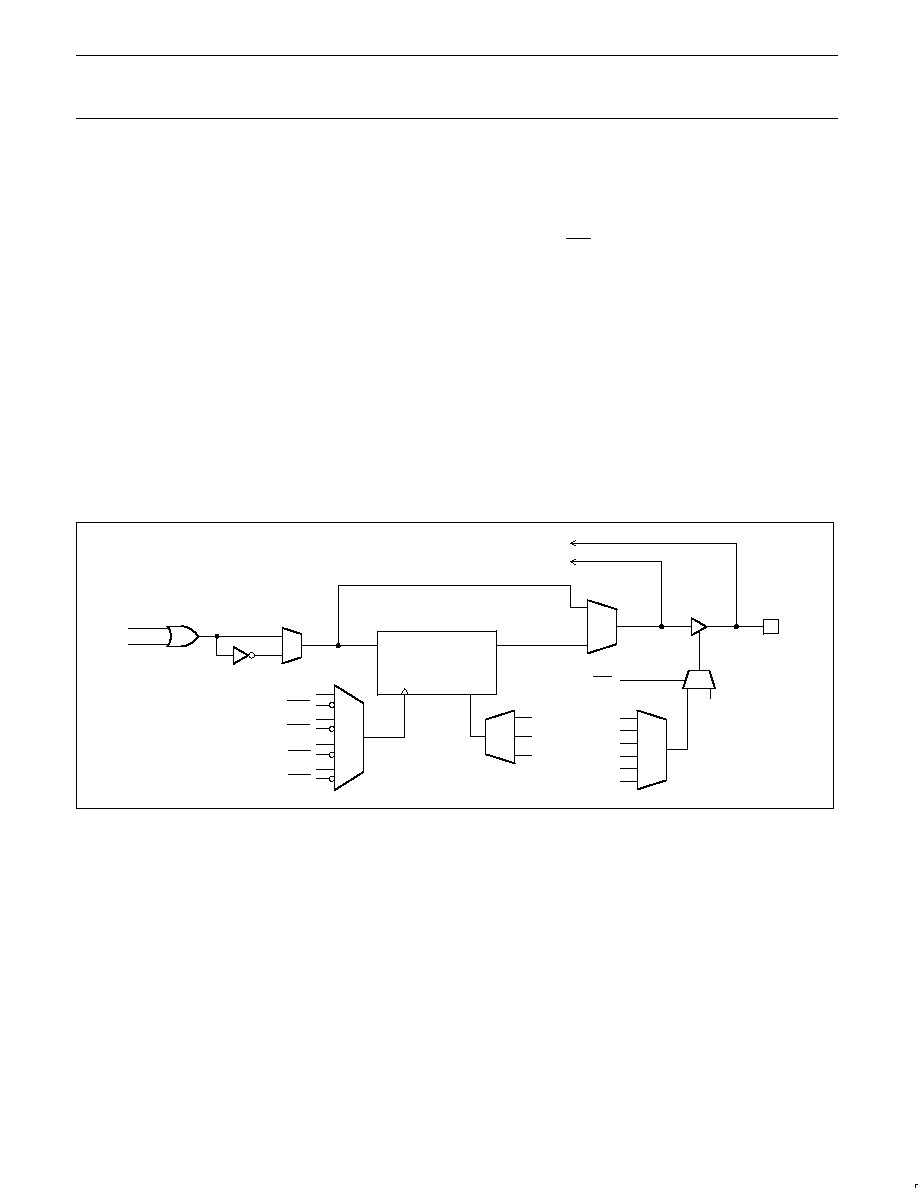
Macrocell Architecture
Figure 3 shows the architecture of the macrocell used in the
CoolRunner
TM
family. The macrocell consists of a flip-flop that can be
configured as either a D or T type. A D-type flip-flop is generally
more useful for implementing state machines and data buffering. A
T-type flip-flop is generally more useful in implementing counters. All
CoolRunner
TM
family members provide both synchronous and
asynchronous clocking and provide the ability to clock off either the
falling or rising edges of these clocks. These devices are designed
such that the skew between the rising and falling edges of a clock
are minimized for clocking integrity. There are 4 clocks available on
the PZ3064 device. Clock 0 (CLK0) is designated as the
"synchronous" clock and must be driven by an external source.
Clock 1 (CLK1), Clock 2 (CLK2), and Clock 3 (CLK3) can either be
used as a synchronous clock (driven by an external source) or as an
asynchronous clock (driven by a macrocell equation).
Two of the control terms (CT0 and CT1) are used to control the
Preset/Reset of the macrocell's flip-flop. The Preset/Reset feature
for each macrocell can also be disabled. Note that the Power-on
Reset leaves all macrocells in the "zero" state when power is
properly applied. The other 4 control terms (CT2≠CT5) can be used
to control the Output Enable of the macrocell's output buffers. The
reason there are as many control terms dedicated for the Output
Enable of the macrocell is to insure that all CoolRunner
TM
devices
are PCI compliant. The macrocell's output buffers can also be
always enabled or disabled. All CoolRunner
TM
devices also provide a
Global Tri-State (GTS) pin, which, when pulled Low, will 3-State all
the outputs of the device. This pin is provided to support "In-Circuit
Testing" or "Bed-of-Nails Testing".
There are two feedback paths to the ZIA: one from the macrocell,
and one from the I/O pin. The ZIA feedback path before the output
buffer is the macrocell feedback path, while the ZIA feedback path
after the output buffer is the I/O pin ZIA path. When the macrocell is
used as an output, the output buffer is enabled, and the macrocell
feedback path can be used to feedback the logic implemented in the
macrocell. When the I/O pin is used as an input, the output buffer
will be 3-Stated and the input signal will be fed into the ZIA via the
I/O feedback path, and the logic implemented in the buried
macrocell can be fed back to the ZIA via the macrocell feedback
path. It should be noted that unused inputs or I/Os should be
properly terminated.
CT2
CT3
CT4
CT5
V
CC
GND
INIT
(P or R)
D/T
Q
CLK0
CLK0
CLK1
CLK1
TO ZIA
GND
CT0
CT1
GND
GTS
CLK2
CLK2
CLK3
CLK3
SP00457
Figure 3.
PZ3064 Macrocell Architecture

Philips Semiconductors
Product specification
PZ3064
64 macrocell CPLD
1997 Mar 05
86
Simple Timing Model
Figure 4 shows the CoolRunner
TM
Timing Model. The CoolRunner
TM
timing model looks very much like a 22V10 timing model in that
there are three main timing parameters, including t
PD
, t
SU
, and t
CO
.
In other competing architectures, the user may be able to fit the
design into the CPLD, but is not sure whether system timing
requirements can be met until after the design has been fit into the
device. This is because the timing models of competing
architectures are very complex and include such things as timing
dependencies on the number of parallel expanders borrowed,
sharable expanders, varying number of X and Y routing channels
used, etc. In the XPLA
TM
architecture, the user knows up front
whether the design will meet system timing requirements. This is
due to the simplicity of the timing model. For example, in the
PZ3064 device, the user knows up front that if a given output uses
5 product terms or less, the t
PD
= 10ns, the t
SU_PAL
= 6ns, and the
t
CO
= 7ns. If an output is using 6 to 37 product terms, an additional
2ns must be added to the t
PD
and t
SU
timing parameters to account
for the time to propagate through the PLA array.
TotalCMOS
TM
Design Technique
for Fast Zero Power
Philips is the first to offer a TotalCMOS
TM
CPLD, both in process
technology and design technique. Philips employs a cascade of
CMOS gates to implement its Sum of Products instead of the
traditional sense amp approach. This CMOS gate implementation
allows Philips to offer CPLDs which are both high performance and
low power, breaking the paradigm that to have low power, you must
have low performance. Refer to Figure 5 and Table 2 showing the I
DD
vs. Frequency of our PZ3064 TotalCMOS
TM
CPLD.
OUTPUT PIN
INPUT PIN
SP00441
t
PD_PAL
= COMBINATORIAL PAL ONLY
t
PD_PLA
= COMBINATORIAL PAL + PLA
CLOCK
OUTPUT PIN
INPUT PIN
D
Q
REGISTERED
t
SU_PAL
= PAL ONLY
t
SU_PLA
= PAL + PLA
REGISTERED
t
CO
Figure 4.
CoolRunner
TM
Timing Model
TYPICAL
I
DD
(mA)
FREQUENCY (MHz)
SP00460A
0
20
40
60
80
100
0
20
40
60
80
100
Figure 5.
I
DD
vs. Frequency @ V
DD
= 3.3V, 25
∞
C
Table 2. I
DD
vs. Frequency
V
DD
= 3.3V
FREQUENCY (MHz)
0
20
40
60
80
100
Typical I
DD
( mA)
0.04
13
26
40
50
63
Philips Semiconductors
Product specification
PZ3064
64 macrocell CPLD
1997 Mar 05
87
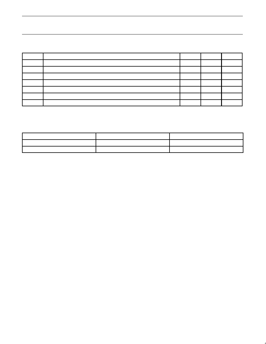
ABSOLUTE MAXIMUM RATINGS
4
SYMBOL
PARAMETER
MIN.
MAX.
UNIT
V
DD
Supply voltage
≠0.5
7.0
V
V
I
Input voltage
≠1.2
V
DD
+0.5
V
V
OUT
Output voltage
≠0.5
V
DD
+0.5
V
I
IN
Input current
≠30
30
mA
I
OUT
Output current
≠100
100
mA
T
J
Maximum junction temperature
≠40
150
∞
C
T
str
Storage temperature
≠65
150
∞
C
NOTES:
4. Stresses above those listed may cause malfunction or permanent damage to the device. This is a stress rating only. Functional operation at
these or any other condition above those indicated in the operational and programming specification is not implied.
OPERATING RANGE
PRODUCT GRADE
TEMPERATURE
VOLTAGE
Commercial
0 to +70
∞
C
3.3
±
10% V
Industrial
≠40 to +85
∞
C
3.3
±
10% V
Philips Semiconductors
Product specification
PZ3064
64 macrocell CPLD
1997 Mar 05
88
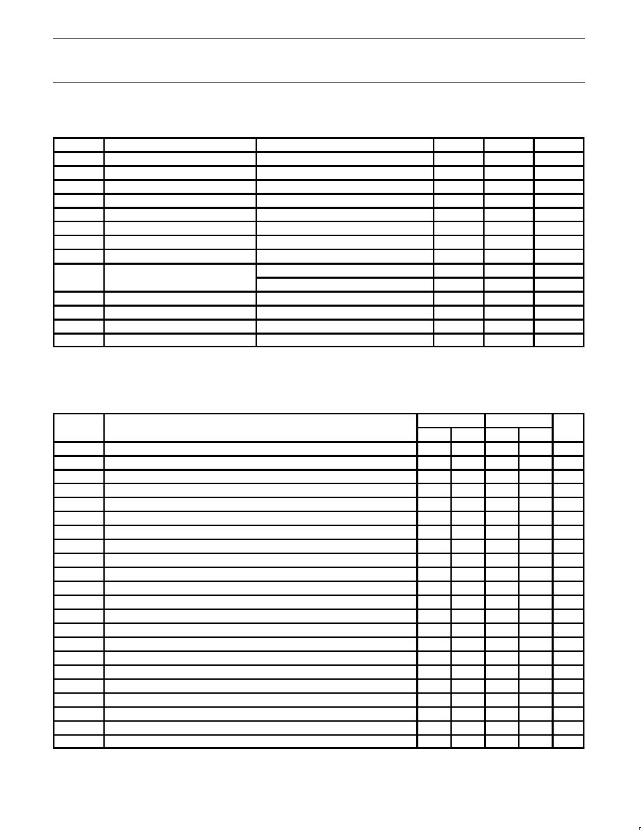
DC ELECTRICAL CHARACTERISTICS FOR COMMERCIAL GRADE DEVICES
Commercial: 0
∞
C
T
amb
+70
∞
C; 3.0V
V
DD
3.6V
SYMBOL
PARAMETER
TEST CONDITIONS
MIN.
MAX.
UNIT
V
IL
Input voltage low
V
DD
= 3.0V
0.8
V
V
IH
Input voltage high
V
DD
= 3.6V
2.0
V
V
I
Input clamp voltage
V
DD
= 3.0V, I
IN
= ≠18mA
≠1.2
V
V
OL
Output voltage low
V
DD
= 3.0V, I
OL
= 8mA
0.5
V
V
OH
Output voltage high
V
DD
= 3.0V, I
OH
= ≠8mA
2.4
V
I
I
Input leakage current
V
IN
= 0 to V
DD
≠10
10
µ
A
I
OZ
3-Stated output leakage current
V
IN
= 0 to V
DD
≠10
10
µ
A
I
DDQ
Standby current
V
DD
= 3.6V, T
amb
= 0
∞
C
50
µ
A
I
1
Dynamic current
V
DD
= 3.6V, T
amb
= 0
∞
C @ 1MHz
1
mA
I
DDD
1
Dynamic current
V
DD
= 3.6V, T
amb
= 0
∞
C @ 50MHz
40
mA
I
OS
Short circuit output current
1 pin at a time for no longer than 1 second
≠5
≠100
mA
C
IN
Input pin capacitance
T
amb
= 25
∞
C, f = 1MHz
8
pF
C
CLK
Clock input capacitance
T
amb
= 25
∞
C, f = 1MHz
5
12
pF
C
I/O
I/O pin capacitance
T
amb
= 25
∞
C, f = 1MHz
10
pF
NOTE:
1. This parameter measured with a 16-bit, loadable up/down counter loaded into every logic block, with all outputs enabled and unloaded.
Inputs are tied to V
DD
or ground. This parameter guaranteed by design and characterization, not testing.
AC ELECTRICAL CHARACTERISTICS
1
FOR COMMERCIAL GRADE DEVICES
Commercial: 0
∞
C
T
amb
+70
∞
C; 3.0V
V
DD
3.6V
SYMBOL
PARAMETER
≠10
≠12
UNIT
SYMBOL
PARAMETER
MIN.
MAX.
MIN.
MAX.
UNIT
t
PD_PAL
Propagation delay time, input (or feedback node) to output through PAL
2
10
2
12
ns
t
PD_PLA
Propagation delay time, input (or feedback node) to output through PAL & PLA
3
12.5
3
14.5
ns
t
CO
Clock to out delay time
2
7
2
8
ns
t
SU_PAL
Setup time (from input or feedback node) through PAL
5.5
7
ns
t
SU_PLA
Setup time (from input or feedback node) through PAL + PLA
8
9.5
ns
t
H
Hold time
0
0
ns
t
CH
Clock High time
4
5
ns
t
CL
Clock Low time
4
5
ns
t
R
Input Rise time
20
20
ns
t
F
Input Fall time
20
20
ns
f
MAX1
Maximum FF toggle rate
2
(1/t
CH
+ t
CL
)
125
100
MHz
f
MAX2
Maximum internal frequency
2
(1/t
SUPAL
+ t
CF
)
91
74
MHz
f
MAX3
Maximum external frequency
2
(1/t
SUPAL
+ t
CO
)
80
67
MHz
t
BUF
Output buffer delay time
1.5
1.5
ns
t
PDF_PAL
Input (or feedback node) to internal feedback node delay time through PAL
8.5
10.5
ns
t
PDF_PLA
Input (or feedback node) to internal feedback node delay time through PAL+PLA
11
13
ns
t
CF
Clock to internal feedback node delay time
5.5
6.5
ns
t
INIT
Delay from valid V
DD
to valid reset
50
50
µ
s
t
ER
Input to output disable
3
12.5
14
ns
t
EA
Input to output valid
12.5
14
ns
t
RP
Input to register preset
15
16
ns
t
RR
Input to register reset
15
16
ns
NOTES:
1. Specifications measured with one output switching. See Figure 6 and Table 3 for derating.
2. This parameter guaranteed by design and characterization, not by test.
3. Output C
L
= 5pF.

Philips Semiconductors
Product specification
PZ3064
64 macrocell CPLD
1997 Mar 05
89
DC ELECTRICAL CHARACTERISTICS FOR INDUSTRIAL GRADE DEVICES
Industrial:
≠40
∞
C
T
amb
+85
∞
C; 3.0V
V
DD
3.6V
SYMBOL
PARAMETER
TEST CONDITIONS
MIN.
MAX.
UNIT
V
IL
Input voltage low
V
DD
= 3.0V
0.8
V
V
IH
Input voltage high
V
DD
= 3.6V
2.0
V
V
I
Input clamp voltage
V
DD
= 3.0V, I
IN
= ≠18mA
≠1.2
V
V
OL
Output voltage low
V
DD
= 3.0V, I
OL
= 8mA
0.5
V
V
OH
Output voltage high
V
DD
= 3.0V, I
OH
= ≠8mA
2.4
V
I
I
Input leakage current
V
IN
= 0 to V
DD
≠10
10
µ
A
I
OZ
3-Stated output leakage current
V
IN
= 0 to V
DD
≠10
10
µ
A
I
DDQ
Standby current
V
DD
= 3.6V, T
amb
= ≠40
∞
C
50
µ
A
I
1
Dynamic current
V
DD
= 3.6V, T
amb
= ≠40
∞
C @ 1MHz
1
mA
I
DDD
1
Dynamic current
V
DD
= 3.6V, T
amb
= ≠40
∞
C @ 50MHz
40
mA
I
OS
Short circuit output current
1 pin at a time for no longer than 1 second
≠5
≠130
mA
C
IN
Input pin capacitance
T
amb
= 25
∞
C, f = 1MHz
8
pF
C
CLK
Clock input capacitance
T
amb
= 25
∞
C, f = 1MHz
5
12
pF
C
I/O
I/O pin capacitance
T
amb
= 25
∞
C, f = 1MHz
10
pF
NOTE:
1. This parameter measured with a 16≠bit, loadable up/down counter loaded into every logic block, with all outputs enabled and unloaded.
Inputs are tied to V
DD
or ground. This parameter guaranteed by design and characterization, not testing.
AC ELECTRICAL CHARACTERISTICS
1
FOR INDUSTRIAL GRADE DEVICES
Industrial:
≠40
∞
C
T
amb
+85
∞
C; 3.0V
V
DD
3.6V
SYMBOL
PARAMETER
I12
I15
UNIT
SYMBOL
PARAMETER
MIN.
MAX.
MIN.
MAX.
UNIT
t
PD_PAL
Propagation delay time, input (or feedback node) to output through PAL
2
12
2
15
ns
t
PD_PLA
Propagation delay time, input (or feedback node) to output through PAL & PLA
3
14.5
3
17.5
ns
t
CO
Clock to out delay time
2
8
2
9
ns
t
SU_PAL
Setup time (from input or feedback node) through PAL
7
8
ns
t
SU_PLA
Setup time (from input or feedback node) through PAL + PLA
9.5
10.5
ns
t
H
Hold time
0
0
ns
t
CH
Clock High time
5
5
ns
t
CL
Clock Low time
5
5
ns
t
R
Input Rise time
20
20
ns
t
F
Input Fall time
20
20
ns
f
MAX1
Maximum FF toggle rate
2
(1/t
CH
+ t
CL
)
100
100
MHz
f
MAX2
Maximum internal frequency
2
(1/t
SUPAL
+ t
CF
)
74
65
MHz
f
MAX3
Maximum external frequency
2
(1/t
SUPAL
+ t
CO
)
67
58
MHz
t
BUF
Output buffer delay time
1.5
1.5
ns
t
PDF_PAL
Input (or feedback node) to internal feedback node delay time through PAL
10.5
13.5
ns
t
PDF_PLA
Input (or feedback node) to internal feedback node delay time through PAL+PLA
13
16
ns
t
CF
Clock to internal feedback node delay time
6.5
7.5
ns
t
INIT
Delay from valid V
DD
to valid reset
50
50
µ
s
t
ER
Input to output disable
3
14
15
ns
t
EA
Input to output valid
14
15
ns
t
RP
Input to register preset
16
17
ns
t
RR
Input to register reset
16
17
ns
NOTES:
1. Specifications measured with one output switching. See Figure 6 and Table 3 for derating.
2. This parameter guaranteed by design and characterization, not by test.
3. Output C
L
= 5pF.

Philips Semiconductors
Product specification
PZ3064
64 macrocell CPLD
1997 Mar 05
90
SWITCHING CHARACTERISTICS
The test load circuit and load values for the AC Electrical Characteristics are illustrated below.
V
DD
V
IN
V
OUT
C1
R1
R2
S1
S2
COMPONENT
VALUES
R1
390
R2
390
C1
35pF
MEASUREMENT
S1
S2
t
PZH
Open
Closed
t
PZL
Closed
Open
t
P
Closed
Closed
NOTE: For t
PHZ
and t
PLZ
C = 5pF
SP00461A
SP00462
NUMBER OF OUTPUTS SWITCHING
1
2
4
8
12
16
V
DD
= 3.3V, 25
∞
C
8.20
8.60
9.00
8.00
8.40
8.80
9.20
9.40
9.60
t
PD_PAL
(ns)
9.80
10.00
Figure 6.
t
PD_PAL
vs. Outputs Switching
Table 3. t
PD_PAL
vs. Number of Outputs Switching
V
DD
= 3.3V
NUMBER OF
OUTPUTS
1
2
4
8
12
16
Typical (ns)
8.0
8.4
8.8
9.2
9.6
10.0
VOLTAGE WAVEFORM
90%
10%
1.5ns
1.5ns
+3.0V
0V
t
R
t
F
MEASUREMENTS:
All circuit delays are measured at the +1.5V level of
inputs and outputs, unless otherwise specified.
Input Pulses
SP00368

Philips Semiconductors
Product specification
PZ3064
64 macrocell CPLD
1997 Mar 05
91
PIN DESCRIPTIONS
PZ3064 ≠ 44-Pin Plastic Leaded Chip Carrier
LCC
6
1
40
7
17
39
29
18
28
Pin
Function
1
IN1
2
IN3
3
V
DD
4
I/O-A0/CK3
5
I/O-A2
6
I/O-A5
7
I/O-A8 (TDI)
8
I/O-A11
9
I/O-A12
10
GND
11
I/O-A13
12
I/O-A15
13
I/O-B15 (TMS)*
14
I/O-B13
15
V
DD
Pin
Function
16
I/O-B10
17
I/O-B8
18
I/O-B4
19
I/O-B3
20
I/O-B2
21
I/O-B0/CK2
22
GND
23
V
DD
24
I/O-C0/CK1
25
I/O-C2
26
I/O-C3
27
I/O-C4
28
I/O-C7
29
I/O-C8
30
GND
Pin
Function
31
I/O-C13
32
I/O-C15 (TCK)
33
I/O-D15
34
I/O-D13
35
V
DD
36
I/O-D12
37
I/O-D11
38
I/O-D8 (TDO)
39
I/O-D7
40
I/O-D2
41
I/O-D0
42
GND
43
IN0-CK0
44
IN2-gtsn
*
THE TEST MODE SELECT (TMS) FUNCTION IS
INACTIVE ON NON-ISR ARCHITECTURES.
SP00452A
PZ3064 ≠ 44-Pin Thin Quad Flat Package
QFP
44
34
1
11
33
23
12
22
Pin
Function
1
I/O-A8
2
I/O-A11
3
I/O-A12
4
GND
5
I/O-A13
6
I/O-A15
7
I/O-B15 (TMS)*
8
I/O-B13
9
V
DD
10
I/O-B10
11
I/O-B8
12
I/O-B4
13
I/O-B3
14
I/O-B2
15
I/O-B0/CK2
Pin
Function
16
GND
17
V
DD
18
I/O-C0/CK1
19
I/O-C2
20
I/O-C3
21
I/O-C4
22
I/O-C7
23
I/O-C8
24
GND
25
I/O-C13
26
I/O-C15 (TCK)
27
I/O-D15
28
I/O-D13
29
V
DD
30
I/O-D12
Pin
Function
31
I/O-D11
32
I/O-D8 (TDO)
33
I/O-D7
34
I/O-D2
35
I/O-D0
36
GND
37
IN0/CK0
38
IN2-gtsn
39
IN1
40
IN3
41
V
DD
42
I/O-A0/CK3
43
I/O-A2
44
I/O-A5
SP00453
*
THE TEST MODE SELECT (TMS) FUNCTION IS
INACTIVE ON NON-ISR ARCHITECTURES.
PZ3064 ≠ 68-Pin Plastic Leaded Chip Carrier
LCC
9
1
61
10
26
60
44
27
43
Pin
Function
1
IN1
2
IN3
3
V
DD
4
I/O-A0/CK3
5
I/O-A2
6
GND
7
I/O-A3
8
I/O-A4
9
I/O-A5
10
I/O-A7
11
V
DD
12
I/O-A8 (TDI)
13
I/O-A10
14
I/O-A11
15
I/O-A12
16
GND
17
I/O-A13
18
I/O-A15
19
I/O-B15 (TMS)*
20
I/O-B13
21
V
DD
22
I/O-B12
23
I/O-B11
Pin
Function
24
I/O-B10
25
I/O-B8
26
GND
27
I/O-B7
28
I/O-B5
29
I/O-B4
30
I/O-B3
31
V
DD
32
I/O-B2
33
I/O-B0/CK2
34
GND
35
V
DD
36
I/O-C0/CK1
37
I/O-C2
38
GND
39
I/O-C3
40
I/O-C4
41
I/O-C5
42
I/O-C7
43
V
DD
44
I/O-C8
45
I/O-C10
46
I/O-C11
Pin
Function
47
I/O-C12
48
GND
49
I/O-D13
50
I/O-C15 (TCK)
51
I/O-D15
52
I/O-D13
53
V
DD
54
I/O-D12
55
I/O-D11
56
I/O-D9
57
I/O-D8 (TDO)
58
GND
59
I/O-D7
60
I/O-D6
61
I/O-D4
62
I/O-D3
63
V
DD
64
I/O-D2
65
I/O-D0
66
GND
67
IN0/CK0
68
IN2-gtsn
*
THE TEST MODE SELECT (TMS) FUNCTION IS
INACTIVE ON NON-ISR ARCHITECTURES.
SP00454
Philips Semiconductors
Product specification
PZ3064
64 macrocell CPLD
1997 Mar 05
92
PZ3064 ≠ 84-Pin Plastic Leaded Chip Carrier
LCC
11
1
75
12
32
74
54
33
53
Pin
Function
1
IN1
2
IN3
3
V
DD
4
I/O-A0/CK3
5
I/O-A1
6
I/O-A2
7
GND
8
I/O-A3
9
I/O-A4
10
I/O-A5
11
I/O-A6
12
I/O-A7
13
V
CC
14
I/O-A8 (TDI)
15
I/O-A9
16
I/O-A10
17
I/O-A11
18
I/O-A12
19
GND
20
I/O-A13
21
I/O-A14
22
I/O-B15
23
I/O-B15 (TMS)*
24
I/O-B14
25
I/O-B13
26
V
DD
27
I/O-B12
28
I/O-B11
Pin
Function
29
I/O-B10
30
I/O-B9
31
I/O-B8
32
GND
33
I/O-B7
34
I/O-B6
35
I/O-B5
36
I/O-B4
37
I/O-B3
38
V
DD
39
I/O-B2
40
I/O-B1
41
I/O-B0/CK2
42
GND
43
V
DD
44
I/O-C0/CK1
45
I/O-C1
46
I/O-C2
47
GND
48
I/O-C3
49
I/O-C4
50
I/O-C5
51
I/O-C6
52
I/O-C7
53
V
DD
54
I/O-C8
55
I/O-C9
56
I/O-C10
Pin
Function
57
I/O-C11
58
I/O-C12
59
GND
60
I/O-C13
61
I/O-C14
62
I/O-C15 (TCK)
63
I/O-D15
64
I/O-D14
65
I/O-D13
66
V
DD
67
I/O-D12
68
I/O-D11
69
I/O-D10
70
I/O-D9
71
I/O-D8 (TDO)
72
GND
73
I/O-D7
74
I/O-D6
75
I/O-D5
76
I/O-D4
77
I/O-D3
78
V
DD
79
I/O-D2
80
I/O-D1
81
I/O-D0
82
GND
83
IN0/CK0
84
IN2-gtsn
*
THE TEST MODE SELECT (TMS) FUNCTION IS
INACTIVE ON NON-ISR ARCHITECTURES.
SP00455
PZ3064 ≠ 100-Pin Plastic Quad Flat Package
Pin
Function
1
NC
2
NC
3
I/O-A6
4
I/O-A7
5
V
DD
6
I/O-A8 (TDI)
7
NC
8
I/O-A9
9
NC
10
I/O-A10
11
I/O-A11
12
I/O-A12
13
GND
14
I/O-A13
15
I/O-A14
16
I/O-A15
17
I/O-B15 (TMS)*
18
I/O-B14
19
I/O-B13
20
V
DD
21
I/O-B12
22
I/O-B11
23
I/O-B10
24
NC
25
I/O-B9
26
NC
27
I/O-B8
28
GND
29
NC
30
NC
31
I/O-B7
32
I/O-B6
33
I/O-B5
34
I/O-B4
Pin
Function
35
I/O-B3
36
V
DD
37
I/O-B2
38
I/O-B1
39
I/O-B0/CK2
40
GND
41
V
DD
42
I/O-C0/CK1
43
I/O-C1
44
I/O-C2
45
GND
46
I/O-C3
47
I/O-C4
48
I/O-C5
49
I/O-C6
50
I/O-C7
51
NC
52
NC
53
V
DD
54
I/O-C8
55
NC
56
I/O-C9
57
NC
58
I/O-C10
59
I/O-C11
60
I/O-C12
61
GND
62
I/O-C13
63
I/O-C14
64
I/O-C15 (TCK)
65
I/O-D15
66
I/O-D14
67
I/O-D13
68
V
DD
Pin
Function
69
I/O-D12
70
I/O-D11
71
I/O-D10
72
NC
73
I/O-D9
74
NC
75
I/O-D8 (TDO)
76
GND
77
I/O-D7
78
I/O-D6
79
NC
80
NC
81
I/O-D5
82
I/O-D4
83
I/O-D3
84
V
DD
85
I/O-D2
86
I/O-D1
87
I/O-D0
88
GND
89
IN0/CK0
90
IN2-gtsn
91
IN1
92
IN3
93
V
DD
94
I/O-A0/CK3
95
I/O-A1
96
I/O-A2
97
GND
98
I/O-A3
99
I/O-A4
100
I/O-A5
*
THE TEST MODE SELECT (TMS) FUNCTION IS
INACTIVE ON NON-ISR ARCHITECTURES.
SP00456
QFP
100
81
1
30
80
51
31
50

Philips Semiconductors
Product specification
PZ3064
64 macrocell CPLD
1997 Mar 05
93
Package Thermal Characteristics
Philips Semiconductors uses the Temperature Sensitive Parameter
(TSP) method to test thermal resistance. This method meets
Mil-Std-883C Method 1012.1 and is described in Philips
1995 IC
Package Databook. Thermal resistance varies slightly as a function
of input power. As input power increases, thermal resistance
changes approximately 5% for a 100% change in power.
Figure 7 is a derating curve for the change in
JA
with airflow based
on wind tunnel measurements. It should be noted that the wind flow
dynamics are more complex and turbulent in actual applications
than in a wind tunnel. Also, the test boards used in the wind tunnel
contribute significantly to forced convection heat transfer, and may
not be similar to the actual circuit board, especially in size.
Package
JA
44-pin PLCC
44.8
∞
C/W
44-pin TQFP
60.8
∞
C/W
68-pin PLCC
44.9
∞
C/W
84-pin PLCC
34.7
∞
C/W
100-pin PQFP
44.5
∞
C/W
0
10
20
30
40
50
0
1
2
3
4
5
PERCENTAGE
REDUCTION IN
JA (%)
AIR FLOW (m/s)
PLCC/
QFP
SP00419A
Figure 7.
Average Effect of Airflow on
JA

Philips Semiconductors
Product specification
PZ3064
64 macrocell CPLD
1997 Mar 05
94
PLCC44:
plastic leaded chip carrier; 44 leads
SOT187-2

Philips Semiconductors
Product specification
PZ3064
64 macrocell CPLD
1997 Mar 05
95
TQFP44:
plastic thin quad flat package; 44 leads; body 10 x 10 x 1.0 mm
SOT376-1

Philips Semiconductors
Product specification
PZ3064
64 macrocell CPLD
1997 Mar 05
96
PLCC68:
plastic leaded chip carrier; 68 leads; pedestal
SOT188-3
Philips Semiconductors
Product specification
PZ3064
64 macrocell CPLD
1997 Mar 05
97
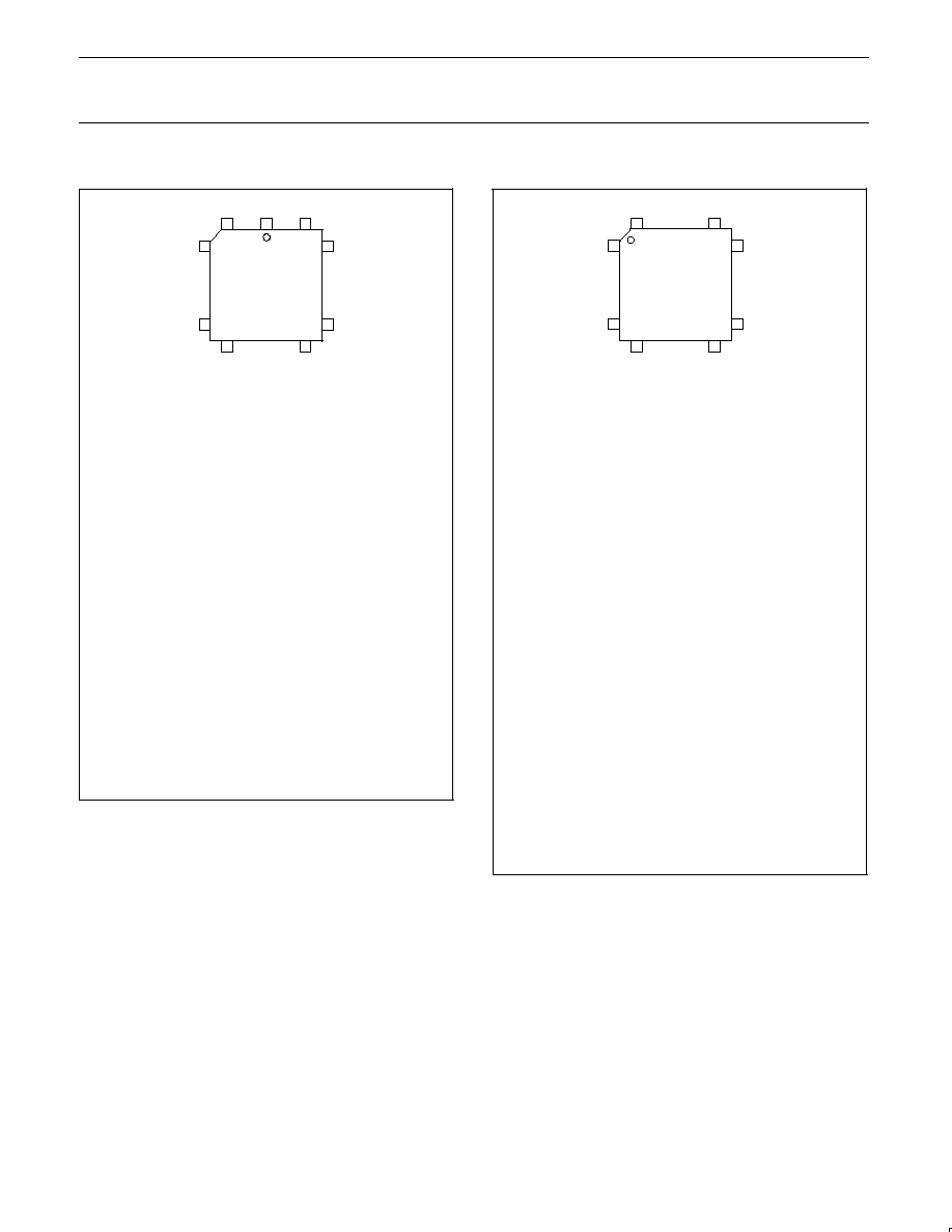
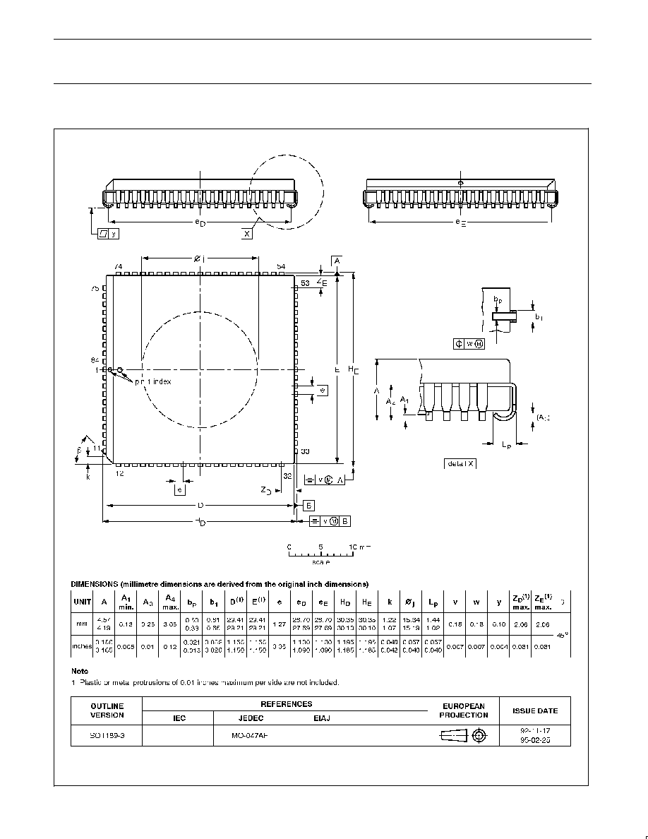
PLCC84:
plastic leaded chip carrier; 84 leads; pedestal
SOT189-3

Philips Semiconductors
Product specification
PZ3064
64 macrocell CPLD
1997 Mar 05
98
QFP100:
plastic quad flat package; 100 leads (lead length 1.6 mm); body 14 x 20 x 2.8 mm
SOT382-1

Philips Semiconductors
Product specification
PZ3064
64 macrocell CPLD
1997 Mar 05
99
NOTES

Philips Semiconductors
Product specification
PZ3064
64 macrocell CPLD
1997 Mar 05
100
Philips Semiconductors and Philips Electronics North America Corporation reserve the right to make changes, without notice, in the products,
including circuits, standard cells, and/or software, described or contained herein in order to improve design and/or performance. Philips
Semiconductors assumes no responsibility or liability for the use of any of these products, conveys no license or title under any patent, copyright,
or mask work right to these products, and makes no representations or warranties that these products are free from patent, copyright, or mask
work right infringement, unless otherwise specified. Applications that are described herein for any of these products are for illustrative purposes
only. Philips Semiconductors makes no representation or warranty that such applications will be suitable for the specified use without further testing
or modification.
LIFE SUPPORT APPLICATIONS
Philips Semiconductors and Philips Electronics North America Corporation Products are not designed for use in life support appliances, devices,
or systems where malfunction of a Philips Semiconductors and Philips Electronics North America Corporation Product can reasonably be expected
to result in a personal injury. Philips Semiconductors and Philips Electronics North America Corporation customers using or selling Philips
Semiconductors and Philips Electronics North America Corporation Products for use in such applications do so at their own risk and agree to fully
indemnify Philips Semiconductors and Philips Electronics North America Corporation for any damages resulting from such improper use or sale.
This data sheet contains preliminary data, and supplementary data will be published at a later date. Philips
Semiconductors reserves the right to make changes at any time without notice in order to improve design
and supply the best possible product.
Philips Semiconductors
811 East Arques Avenue
P.O. Box 3409
Sunnyvale, California 94088≠3409
Telephone 800-234-7381
DEFINITIONS
Data Sheet Identification
Product Status
Definition
Objective Specification
Preliminary Specification
Product Specification
Formative or in Design
Preproduction Product
Full Production
This data sheet contains the design target or goal specifications for product development. Specifications
may change in any manner without notice.
This data sheet contains Final Specifications. Philips Semiconductors reserves the right to make changes
at any time without notice, in order to improve design and supply the best possible product.
©
Copyright Philips Electronics North America Corporation 1997
All rights reserved. Printed in U.S.A.
Philips
Semiconductors