 | –≠–ª–µ–∫—Ç—Ä–æ–Ω–Ω—ã–π –∫–æ–º–ø–æ–Ω–µ–Ω—Ç: SA2400ABE | –°–∫–∞—á–∞—Ç—å:  PDF PDF  ZIP ZIP |
Document Outline
- 1. DESCRIPTION
- 2. FUNCTIONAL BLOCKS AND FEATURES
- 3. APPLICATIONS
- 4. BLOCK DIAGRAM
- 5. PINNING INFORMATION
- 6. FUNCTIONAL DESCRIPTION
- 7. OPERATING CONDITIONS
- 8. OPERATIONAL MODES AND CURRENT CONSUMPTION
- 9. SA2400A RECEIVER
- 9.1 AGC handshake and timing
- 10. SA2400A TRANSMITTER
- 11. VCO AND SYNTHESIZER
- 12. FUNCTIONAL DESCRIPTION
- 13. SA2400A OTHER FUNCTIONALITY
- 14. 3-WIRE BUS/LOGIC CONTROL
- 14.1 Description of WRITE cycle
- 14.2 Description of READ cycle
- 14.3 3-wire bus/logic control AC characteristics
- 14.4 3-wire bus control register map
- 14.5 Fast serial interface for ReceiverÖAGC
- 14.6 Fast serial interface AC characteristics
- 15. PERFORMANCE CURVES
- PACKAGE UTLINE
- REVISION HISTORY
- Data sheet status
- Definitions
- Disclaimers

Philips
Semiconductors
SA2400A
Single chip transceiver for
2.45 GHz ISM band
Product data
2002 Nov 04
INTEGRATED CIRCUITS

Philips Semiconductors
Product data
SA2400A
Single chip transceiver for 2.45 GHz ISM band
2
2002 Nov 04
853-2320 28727
1. DESCRIPTION
The SA2400A is a fully integrated single IC RF transceiver designed
for 2.45 GHz wireless LAN (WLAN) applications. It is a direct
conversion radio architecture that is fabricated on an advanced
30 GHz f
T
BiCMOS process. The SA2400A combines a receiver,
transmitter, and LO generation into a single IC. The receiver
consists of a low-noise amplifier, down-conversion mixers, fully
integrated channel filters, and an Automatic Gain Control (AGC) with
an on-chip closed loop. The transmitter contains power ramping,
filters, up-conversion, and pre-drivers. The LO generation is formed
by an entirely on-chip VCO and a fractional-N synthesizer.
Typical system performance parameters for the receiver are 93 dB
gain, 7.5 dB noise figure, input-referred third-order intercept point
(IIP3) of +1 dBm, AGC settling time of 8
µ
s, and Tx-to-Rx switching
time of 3
µ
s. The transmitter typical system performance parameters
are an output power range from ≠7 dBm to +8 dBm in 1 dB steps,
≠40 dBc carrier leakage after calibration, 22 dB sideband
suppression, in-band common mode rejection of 30 dB, and
Rx-to-Tx switching time of 3
µ
s.
2. FUNCTIONAL BLOCKS AND FEATURES
The block diagram of the SA2400A Direct Conversion transceiver is
given in Figure 1. It consists of the following functional blocks:
∑
A 79 dB adjustable gain range direct conversion zero IF receiver
with 3
µ
s (typical) Tx to Rx switching time, and comprising the
following:
≠ Front-end LNA with two internal gain states
≠ A fast on-chip closed loop composite RF and IF AGC with
zoomed analog RSSI output and 8
µ
s settling time
≠ Quadrature downconverters from 2.45 GHz RF directly to
zero IF
≠ On-chip fast baseband DC cancellation with automatically
stepped bandwidths of 10 MHz, 1 MHz, 100 kHz, and 10 kHz,
settling within 8≠13
µ
s for a DC error of 10% that decays to 1%.
≠ Fully integrated channel filters, appropriate for 11 Msymbols/s
QPSK modulation RF bandwidth.
∑
An I/Q upconverter from baseband directly to 2.45 GHz, with
+8 dBm output power, ≠40 dBc typical carrier leakage (calibrated)
and 3
µ
s (typical) Rx to Tx switching time, and comprising the
following:
≠ Wide band IQ modulator producing better than 14% EVM for
11 Msymbols/s QPSK modulation
≠ Integrated reconstruction and spectral shaping filters at I and Q
modulation input that is driven by an external D/A. High
common mode rejection to input ground bounce.
≠ FIR-DACs for digital I/Q input feeding the analog signal path
and including additional filtering for spectral shaping.
≠ 2.45 GHz power amplifier driver with +8 dBm maximum output,
15 dB adjustable gain in 1 dB steps and a second switched
output at ≠1.5 dBm power level with similar gain adjustments
that are set by a separate register.
≠ Completely on-chip calibration for Carrier Leakage
compensation.
≠ Internal power ramping with 2
µ
s delay and 0.5
µ
s ramp-up
time.
∑
A fractional-N frequency synthesizer with on-chip VCO and XO
∑
A 3-wire bus for control of most blocks
∑
An additional high speed 3-wire bus for full control of Rx-Gain and
DC-offset compensation parameters with 44Mbits/s.
∑
Fast Tx-Rx switching based on a single digital input pin.
∑
Reference currents and voltage for supply of Baseband Processor
and PA-chip.
3. APPLICATIONS
∑
IEEE 802.11 and 802.11b radios
≠ Supports DSSS and CCK modulation
≠ Supports data rates: 1, 2, 5.5, and 11 Mbps
∑
2.45 GHz ISM band wireless communication devices
Table 1. Ordering Information
TYPE NUMBER
PACKAGE
TYPE NUMBER
NAME
DESCRIPTION
VERSION
SA2400ABE
LQFP48
plastic low profile quad flat package; 48 leads; body 7 x 7 x 1.4 mm
SOT313-2
Philips Semiconductors
Product data
SA2400A
Single chip transceiver for 2.45 GHz ISM band
2002 Nov 04
3
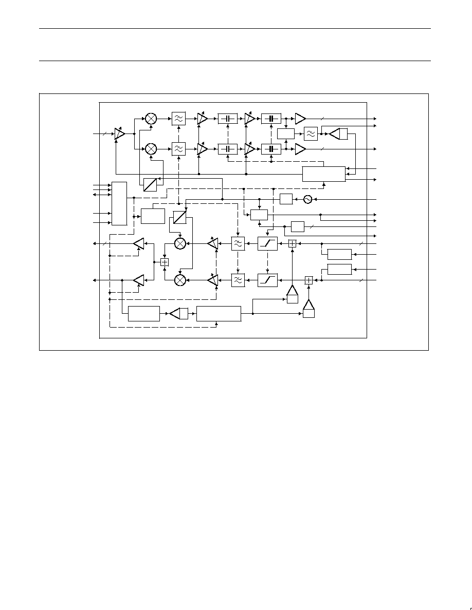
4. BLOCK DIAGRAM
AGC
STATE MACHINE
2
RF_IN
2
RSSI
A/D
2
RX_OUT_I
RSSI
RX_OUT_Q
AGCSET
AGCRESET
0
90
CONTROL
SEN
SCLK
SDATA
TXRX
TX_HI
FILTER
TUNING
0
90
TX_OUT_HI
TX_OUT_LO
2
POWER
DETECTOR
A/D
TXCAL
STATE MACHINE
PLL
CP
: 2
D/A
V_TUNE
XTAL
D/A
XO
REF_CLK
2
LOCK
FIRDAC
FIRDAC
TX_IN_I
DATA_I
DATA_Q
TX_IN_Q
2
2
SR02386
Figure 1.
SA2400A functional block diagram.
Philips Semiconductors
Product data
SA2400A
Single chip transceiver for 2.45 GHz ISM band
2002 Nov 04
4
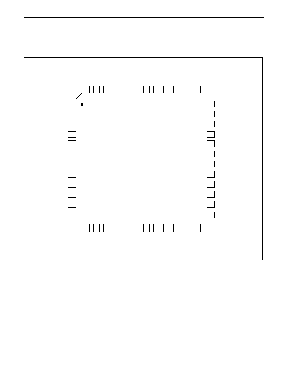
5. PINNING INFORMATION
SR02387
A_GND
TX_HI
A_V
TX_OUT_LO
SA2400A
DD
A_GND
TX_OUT_HI_P
TX_OUT_HI_M
A_GND
SEN
SDA
T
A
SCLK
TX/RX
TX_IN_I_P/
TX_DATA_I
TX_IN_I_M/
TX_DATA_Q
TX_IN_Q_P
TX_IN_Q_M
RX_OUT_Q_P
RX_OUT_Q_M
RX_OUT_I_P
RX_OUT_I_M
D_GND
REF_CLK_OUT
PLL_GND
AGCRESET
AGCSET
IDCOUT
A_GND
GND_LNA
RF_IN_P
RF_IN_N
GND_LNA
TEST1
TEST2
V_2P5
A_V
DD
A_V
DD
RSSI
V_TUNE
VCO_V
VCO_P
VCO_M
_PLL
CP
LOCK
XT
AL_1
XT
AL_2
D_V
DD
VCO_GND
DD
V
DD
1
2
3
4
5
6
7
8
9
10
11
12
13
14
15
16
17
18
19
20
21
22
23
24
48
47
46
45
44
43
42
41
40
39
38
37
36
35
34
33
32
31
30
29
28
27
26
25
Figure 2.
Pin configuration.
Philips Semiconductors
Product data
SA2400A
Single chip transceiver for 2.45 GHz ISM band
2002 Nov 04
5
Table 2. Pin description
PIN type is designated by A = Analog, D = Digital, I = Input, O = Output
SYMBOL
PIN
DESCRIPTION
TYPE
AGCRESET
1
AGC start input
DI
AGCSET
2
AGC settled output
DO
IDCOUT
3
Tx-mode:
DC reference current
AO
A_GND
4
Analog Ground
GND_LNA
5
Analog Ground
RF_IN_P
6
RF input (positive)
AI
RF_IN_N
7
RF input (negative)
AI
GND_LNA
8
Analog Ground
A_V
DD
9
Analog Supply
TEST_1
10
Test pin
TEST_2
11
Test pin
V_2P5
12
DC reference voltage
AO
RSSI
13
RSSI output signal
AO
D_V
DD
14
Digital Supply
V_TUNE
15
VCO tuning voltage
AI
VCO_GND
16
VCO ground
VCO_V
DD
17
VCO Supply
VCO_P
18
VCO output/
External VCO input
AI/O
VCO_M
19
VCO output/
External VCO input
AI/O
V
DD
_PLL
20
Synthesizer Supply
CP
21
Charge pump output
AO
LOCK
22
Synthesizer lock indicator
AO
XTAL_1
23
Crystal input
AI
XTAL_2
24
Crystal input
AI
SYMBOL
PIN
DESCRIPTION
TYPE
PLL_GND
25
Synthesizer Ground
REF_CLK_OUT
26
Reference clock output
AO
D_GND
27
Digital and Analog Ground
RX_OUT_I_M
28
Receive output
AO
RX_OUT_I_P
29
Receive output
AO
RX_OUT_Q_M
30
Receive output
AO
RX_OUT_Q_P
31
Receive output
AO
A_V
DD
32
Analog Supply
TX_IN_Q_M
33
Transmit input
AI
TX_IN_Q_P
34
Transmit input
AI
TX_IN_I_M/
TX_DATA_Q
35
Transmit input
AI/DI
TX_IN_I_P/
TX_DATA_I
36
Transmit input
AI/DI
TX/RX
37
Tx/Rx mode select
DI
SCLK
38
Three-wire bus clock
DI
SDATA
39
Three wire bus data
DI/O
SEN
40
Three wire bus enable
DI
A_GND
41
Analog Ground
TX_OUT_HI_M
42
Transmit output, high power
AO
TX_OUT_HI_P
43
Transmit output, high power
AO
A_GND
44
Analog Ground
TX_OUT_LO
45
Transmit output, low power
AO
A_V
DD
46
Analog Supply
TX_HI
47
Transmit output power level
select
DI
A_GND
48
Analog Ground

Philips Semiconductors
Product data
SA2400A
Single chip transceiver for 2.45 GHz ISM band
2002 Nov 04
6
6. FUNCTIONAL DESCRIPTION
The SA2400A transceiver is intended for operation in the 2.45 GHz
band, specifically for IEEE 802.11b 1 and 2 Mbits/s DSSS, and
5.5 and 11 Mbits/s CCK standards. Throughout this document, the
operating RF frequency refers to the ISM band between 2.4 GHz
and 2.5 GHz.
6.1 RF VCO
The local oscillator is common to both the transmitter and the
receiver. The RF VCO is a differential 4.8 GHz oscillator with the
frequency determining components internal to the IC. The VCO is
connected internally to a frequency divider and a quadrature
generator circuit which produces the LO for the IQ up- and
downmixer. The divider output is also internally connected to the
synthesizer, which can be programmed in order to produce steps of
0.5 MHz for the desired LO frequency.
At the time of power-up, the VCO must be calibrated by invoking the
VCOCALIB mode by means of the three-wire bus. This operation
will select an appropriate frequency band in the VCO, thus
compensating for process tolerances. The calibration takes up to
2.2 ms, after which the IC automatically enters the SLEEP mode.
The synthesizer registers 0x00 through 0x03 must be
re-programmed after completing the VCOCALIB.
The 2.45 GHz LO can also be injected externally.
6.2 RF Low Noise Amplifier
The RF LNA has differential inputs and an external balun is needed
in the case of single-ended operation. It has two gain states which
are controlled internally by the on-chip automatic gain control, or
manually via the 3-wire bus.
6.3 Downconversion mixers
The RF signal is converted down directly to baseband by quadrature
image-reject mixers.
6.4 Receiver low-pass filter, baseband amplifiers
The I and Q low-pass filters are fully integrated Chebychev active
filters. The I and Q pass band extends from DC to a ≠3 dB corner at
7 MHz.
Additional adjustable gain is provided in baseband amplifiers to
achieve a total adjustable gain range of 79 dB. The Rx output is
provided in the form of differential I and Q signals, which must be
DC coupled to the ADC inputs on a base band IC.
6.5 DC cancellation
The Rx chain also integrates a high-pass filter (DC notch) for
cancellation of the DC offset inherent to zero-IF operation. The
high-pass filter has a programmable lower 3 dB cutoff frequency of
10 MHz, 1 MHz, 100 kHz or 10 kHz. The DC offset cancellation
occurs simultaneously with the AGC settling process. During the
AGC settling phase (see below) the cutoff frequency is dynamically
selected between 10 MHz and 1 MHz to quickly reduce DC offset
values from +50 dBc to below ≠20 dBc relative to a ≠76 dBm
antenna input signal before the RSSI (see below) is internally
sampled. After the AGC settling, the high pass is configured for
100 kHz for 5
µ
s before switching to a final 10 kHz cutoff frequency.
The low value of 10 kHz is required for minimizing the signal
distortion created by a high-pass function at zero frequency. The
high-pass will then remain set to the 10 kHz cutoff frequency until a
new AGC cycle is started.
Whenever there is a frequency change in the high-pass filter lower
cutoff, the DC offset can change from a very low value to about 50%
(1 MHz
100 kHz step) or 10% (100 kHz
10 kHz step) of the
signal level. This DC offset then decays according to the high-pass
response of the filter.
The cutoff frequency of the high-pass filter can also be selected
manually by using the RXMGC mode.
6.6 AGC
The receiver contains a fully integrated Automatic Gain Control loop.
It works by adjusting the internal gain such that the Rx output
amplitude, as measured by the RSSI (see below), meets a
predefined target value.
By default, the AGC is always set to a default maximum gain
(adjustable by register value GMAX) whenever the SA2400A enters
the RECEIVE mode of operation from another operational mode. It
takes 5
µ
s for the receiver to settle when it enters this mode, which
includes the time for DC offsets to be removed with a 1 MHz lower
cut-off frequency of the high-pass filtering. This lower cut-off
frequency of 1 MHz remains unchanged as long as the AGC
remains in the default maximum gain state.
The AGC must be invoked by providing a 0-to-1 transition on the
AGCRESET pin, and keeping the signal on that pin to 1 for at least
5
µ
s.
By successively reducing the gain from its initial maximum value,
the loop searches for the correct gain value to provide a nominal
output amplitude of 500 mV
peak, differential
for a QPSK signal (within
±
3 dB dynamic error) at the output pins. This is achieved after a
maximum of 8
µ
s. This time is defined by wait periods necessary to
settle the receiver after gain switching actions. The individual wait
periods can be adjusted by means of register settings.
After completing the AGC settling process, the AGCSET pin is set to
1 by the algorithm. The receiver gain then will not change again until
another pulse is issued on the AGCRESET pin.
For a subsequent AGC operation, the receiver needs to enter its
maximum gain state again. If another AGCRESET signal (as
described above) is issued, the settling period will take an extra
3
µ
s, up to a total of 11
µ
s, since the first 3
µ
s will be spent on
entering maximum gain mode and settling the receiver thereafter. To
shorten this operation, the receiver can be forced to maximum gain
(e.g., at a time when no signal is present) by issuing a 0≠1≠0 pulse
of maximum 1
µ
s pulse width on the AGCRESET pin. The receiver
will then enter maximum gain mode (the AGCSET signal will not be
set to 1 after this), and a following 0-to-1 transition on the
AGCRESET pin will start the settling sequence from maximum gain,
which will then take a maximum of 8
µ
s.
The receiver gain can also be selected manually by using the
RXMGC mode.
The settling target can be adjusted by
±
7 dB from the nominal level
of 500 mV
peak, differential
by means of register settings.
Note: When doing measurements with a single-tone RF signal, the
amplitude at the Rx outputs after settling the AGC will be lower, at
about 300 mV
peak, differential
.

Philips Semiconductors
Product data
SA2400A
Single chip transceiver for 2.45 GHz ISM band
2002 Nov 04
7
6.7 AGC Handshake
On the digital input pin AGCRESET, a 0-to-1 transition clears
AGCSET output to logic 0 and starts the AGC cycle. At the end of
the AGC settling, the AGCSET output is asserted to logic 1. The
AGCRESET input can then be reset to logic 0. At any time in the
RECEIVE mode the AGC can be forced to the maximum gain by
giving the AGCRESET signal as described, but by additionally
re-setting it to logic 0 within 1
µ
s. The AGCSET indication is not
given in this case and the receiver settling time is 3
µ
s. The channel
filters will be set to have a lower cut-off of 1 MHz. For a timing
diagram, please see the receiver parameters section.
6.8 RSSI
The Receive Signal Strength Indicator (RSSI) is implemented as an
error signal comparing the signal level at the Rx output to the
nominal value of 500 mV
peak,differential
. It has a ≠10 dBc to +10 dBc
operational range relative to the nominal signal level. Since the
RSSI acts on the modulated RF signal envelope that is extracted
from the baseband I and Q signals, it includes DC offsets, and will
therefore show transient decaying errors when the AC coupling
lower cut-off frequency is changed.
The RSSI signal reflects on a logarithmic scale the amplitude of the
instantaneous modulated RF signal (envelope). The RSSI signal is
filtered by a low-pass filter with 0.5 MHz upper cut-off frequency.
The SA2400A receiver is designed to give at least ≠10 dBc RSSI at
maximum gain, when there is no signal present, i.e., with only
thermal noise. However, due to process spreads (e.g., gain, noise
figure, IQ low-pass filter bandwidth, etc.), the RSSI may show higher
than ≠10 dBc. In case a calibration is required for setting this noise
power to ≠10 dBc, the AGC's maximum gain (GMAX) can be
changed in the range of 85 to 54 dB in steps of 1 dB via register
settings. The programmed value of maximum gain is never altered
by the AGC settling or by forcing the AGC to maximum gain. Only
the RXMGC mode can set the AGC gain to values higher than
GMAX. The RXMGC mode does not change the value of GMAX.
6.9 Receiver blocking immunity
The receiver is designed to exceed the IEEE802.11 specifications
for the blocking and intermodulation. It can accept continuous or
randomly pulsed interfering single- or multi-tone signals that are
more than 35 dB stronger than the wanted signal, and up to
≠10 dBm of interference level. The spurious I and Q outputs are
maintained to smaller than ≠20 dBc of the wanted signal level.
6.10 Transmitter and IQ upconverter
The transmitter inputs are designed to be driven from a Baseband
IC in one of two modes: a) in analog mode, differential I and Q
inputs expect current signals driven by DACs in the Baseband IC; or
b) in digital mode, single-ended inputs expect two binary data
streams. In this case, integrated FIR≠DACS provide additional
filtering. The data streams are sampled with the reference clock. For
timing specifications, please see the transmitter parameters section.
The wide band IQ upconverter includes spectral shaping
reconstruction filters (4
th
order low-pass Butterworth with 9.75 MHz
3 dB upper cut-off frequency).
At +8 dBm maximum transmitter output level the out-of-band (FCC
forbidden band) spurious signal power is less than ≠77 dBc
(integrated over 1 MHz with a 100 kHz resolution bandwidth) for the
11 Msymbols/sec CCK modulation (footnote
1
). This implies that the
spectral regrowth is dominated by any external PA that may be used
to boost the transmission power level.
In analog mode, it is assumed that the input baseband IQ signals as
delivered from the Baseband IC are pulse shaped.
By using the on-chip calibration loop, the transmitter Carrier
Leakage can be reduced to levels far less than required by the
standard. An RF power meter detects the LO level, converts it into a
digital signal and a state machine determines the compensation
values which are fed through a DAC directly to the IQ inputs. This
mode is activated by setting the IC into the DCALIB mode by means
of 3-wire bus programming. This calibration is designed to
compensate for any DC offsets delivered by the ADCs on the
Baseband IC. The DCALIB cannot be used when the IC is using the
digital-input Tx mode.
The IQ gain and phase imbalance, reconstruction filter roll-off and
in-channel noise produce a modulation EVM of less than 12% for
11 Msymbols/sec QPSK. The transmitter has two switched outputs,
one with ≠1.5 dBm output power and the other one with +8 dBm
output power. The input pin TX_HI is used to select between the two
RF output ports.
The 8 dBm output port is differential and is designed to work
seamlessly (no external filtering required) with the SA2411 power
amplifier.
Upon entering the Tx mode, the ramping up of the RF Tx signal is
delayed by an internal power ramping circuit. The ramping up time is
fixed, while the delay prior to ramping up can be programmed by
register settings.
Note: When switching out of the Transmit mode (either into Receive
mode by transition on TXRX pin, or into another mode by 3-wire
programming), the reference clock input (pins XTAL_1 and XTAL_2)
needs to be active since a digital timer is being used.
6.11 Reference current and voltage outputs
The IC provides a temperature-constant reference current of 1 mA
or 300
µ
A (selectable), active in Tx mode, as well as a 2.5 V
reference voltage.
1.
For a CCK signal, the peak signal power is 21.7 dB lower than the total power integrated over the 22 MHz band. The SA2400A guarantees better than 56 dBc
suppression of the second sidelobe (greater than 22 MHz frequency offset). Consequently, the power level in the forbidden bands is at least 77 dBc below the transmitted
integrated power.

Philips Semiconductors
Product data
SA2400A
Single chip transceiver for 2.45 GHz ISM band
2002 Nov 04
8
7. OPERATING CONDITIONS
Table 3. Absolute Maximum Ratings
Symbol
Parameter
Min
Max
Unit
T
stg
Storage temperature
≠55
+150
∞
C
V
DD
Supply voltage
≠0.5
+3.85
V
Voltage applied to inputs
≠0.5
V
DD
+0.5
V
Short circuit duration, to GND or V
DD
≠
1
second
Table 4. Recommended Operating Conditions
Symbol
Parameter
Min
Nom
Max
Units
T
amb
Ambient operating temperature (Note 1)
≠30
≠
+85
∞
C
V
DD
Supply voltage
2.85
3.3
3.6
V
NOTE:
1. When the digital input mode is used, the lower limit of the ambient operating temperature is higher than ≠30
∞
C. Preliminary characterization
results suggest a limit of ≠20
∞
C. This does not apply if the analog input mode is used.
8. OPERATIONAL MODES AND CURRENT CONSUMPTION
(See also Table 18).
Table 5. Operational modes and current consumption
T
amb
= 25
∞
C; V
CC
= 3.3 V.
Main mode
Duration
Current (mA)
Chip state
Main mode
(register 0x04)
Other conditions
Description
Duration
(max.)
Min
Typ
Max
POWER-UP
SLEEP
XO on,
clock output on
n/a
1.8
2.2
2.7
SLEEP
SLEEP
XO off
Note 1.
n/a
≠
≠
0.05
TX HI
TX/RX or
FASTTXRXMGC
TXRX = HIGH;
TX_HI = HIGH
Synthesizer ON.
Transmitter ON with 8 dBm driver.
Maximum gain.
n/a
120
143
170
TX LO
TX/RX or
FASTTXRXMGC
TXRX = HIGH;
TX_HI = LOW
Synthesizer ON.
Transmitter ON with ≠1.5 dBm driver.
Maximum gain.
n/a
81
95
105
RX
TX/RX or
RXMGC or
FASTTXRXMGC
TXRX = LOW
Synthesizer ON. Receiver ON.
Receiver gain control by:
∑
TX/RX
internal AGC
∑
RXMGC
3-wire bus programming
∑
FASTTXRXMGC
fast 3-wire bus
n/a
81
95
105
WAIT
WAIT
Only Synthesizer and Xtal oscillator ON
n/a
27
31
34
FCALIB
FCALIB
Calibrates cut-off frequency of Tx and Rx
filters internally. Automatic transition to
SLEEP mode upon completion.
3
µ
s
≠
n/a
≠
DCALIB
DCALIB
Maintain TX mode
for 5
µ
s before
calibration.
Quiescent IQ input.
Analog mode used.
Calibration to reduce transmitter carrier
leakage. Automatic transition to SLEEP
mode upon completion.
20
µ
s
≠
n/a
≠
VCOCALIB
VCOCALIB
Calibrates internal VCO.
2200
µ
s
≠
n/a
≠
RESET
RESET
Resets IC into power-up state (SLEEP
mode and all registers at default values)
n/a
≠
n/a
≠
NOTE:
1. All digital inputs connected to GND or V
DD
.

Philips Semiconductors
Product data
SA2400A
Single chip transceiver for 2.45 GHz ISM band
2002 Nov 04
9
8.1 RESET
Shuts down all blocks except the 3-wire digital section, and
programs internal registers to known default values that are
described in section 13. This ensures that the SA2400A transmitter,
receiver, synthesizer and other blocks enter a known state when
made active. The SA2400A enters the SLEEP state automatically
after the RESET state. Before entering either the TXRX or RXMGC
active states, the internal registers can be reprogrammed to change
their values from the default values. A power-up of the digital supply
also forces the SA2400A to the RESET mode.
8.2 SLEEP
All blocks (except the xtal osc) are OFF. The xtal osc can be
separately shut down. Note that the 3-wire bus will remain
operational in all modes as long as the digital supply is ON. The
SA2400A retains programmed values of all active modes when it
comes out of the sleep mode. This includes the synthesizer
operation. Programmed via 3-wire bus.
8.3 WAIT
The PLL is on. Receiver and the transmitter are both OFF. This
mode is useful for a quick turn-around to either TXRX or RXMGC
modes. Transition to or from this mode is done via the 3-wire bus.
8.4 RXMGC
Only the PLL and Receiver are operating. The AGC gain is manually
set by the value of a register field.
8.5 TXRX
In this mode the logic level on the TX/RX input pin determines the
operational mode: 1 = TRANSMIT, 0 = RECEIVE. This way, no
3-wire bus programming is necessary to switch between Tx and Tx,
resulting in faster switching. When entering the RECEIVE mode
(either via 3-wire programming to TXRX mode with TX/RX pin at
logic zero, or by a 1-to-0 transition of TX/RX pin when already in the
TXRX mode), the Receiver is set to maximum gain. An AGC cycle is
initiated by a 0-to-1 change on the AGC_RESET digital input pin. At
any time in the RECEIVE mode, the AGC can be forced to the
maximum gain setting by giving a 1
µ
s pulse on the AGC_RESET
input while the TX/RX input is held at logic 0.
8.6 FASTTXRXMGC
It is similar to the RXMGC mode, except that the manual AGC gain
programming can be done faster, as described in Section 14.5.
8.7 FCALIB
This mode needs to be programmed after power ON in order to
internally calibrate the cut-off frequency of the on-chip transmit and
receive active filters. Upon completion of the calibration, the IC will
automatically switch to Main Mode = SLEEP. This calibration takes a
maximum of 3
µ
s measured from the end of the programming
sequence. The result of this calibration can be read out from register
word 0x04.
8.8 DCALIB
If the analog Tx inputs are used, this mode needs to be programmed
at least once after power ON in order to reduce the transmitter
carrier leakage. This mode should be programmed after being in TX
mode for at least 5
µ
s. Upon completion of the calibration, the IC will
automatically switch to Main Mode = SLEEP. This calibration takes a
maximum of 20
µ
s measured from the end of the programming
sequence. The result of this calibration can be read out from register
0x07.
8.9 VCOCALIB
This mode needs to be programmed at least once after power ON in
order to calibrate the internal VCO. Upon completion of the
calibration, the IC will automatically switch to Main Mode = SLEEP.
This calibration takes a maximum of 2.2 ms from the end of the
programming sequence. After this calibration, the synthesizer must
be re-programmed by writing the register words 0x00 through 0x03.
The result of this calibration can be read out from register 0x08.
Philips Semiconductors
Product data
SA2400A
Single chip transceiver for 2.45 GHz ISM band
2002 Nov 04
10
9. SA2400A RECEIVER
The baseband output signal extends from DC to 8 MHz, and the out-of-band frequency begins from 11 MHz. The modulated test signal used is
11 Msymbols/sec QPSK with raised cosine filtering (50% excess bandwidth for 11 Msymbols/sec). The LO frequency is the same as the
Receiver channel center frequency, as the IF output is at 0 Hz.
Table 6. SA2400A Receiver properties
T
amb
= 25
∞
C; V
CC
= 3.3 V; f
LO
= 2.45 GHz.
Specification
Conditions
Min
Typ
Max
Units
RF input frequency range
Typical
2.4
2.5
GHz
S11 (RF input)
Incl balun+matching. 50
unbalanced. Note 3.
LNA in high gain (see reg. description 0x06)
≠10
≠
dB
LNA in low gain
≠7
≠
dB
Maximum Rx voltage gain
RF input to I or Q outputs
90
93
≠
dB
Max RF input level
Including application, AGCTARGET = +5. Note 1.
≠10
≠
≠
dBm
To maintain nominal IQ output levels as defined
below ("nominal I and Q output voltage")
≠20
≠
≠
dBm
IQ Output DC error (relative to signal,
5
µ
s after AGC set)
≠80 dBm < P
input
< ≠20 dBm, 1 MHz sinewave
output. Note 3.
≠
≠
≠20
dBc
AGC settling time
(indicated by AGC_SET digital
output)
Initiated by AGC_RESET input. Constant RF input
within this settling time. Begins after TX to RX
switching time. Measured from AGC_RESET 0≠1
transition. AGC delay registers (0x05) at default or
smaller values. Note 2.
a) First instance
≠
≠
8
µ
s
b) 2
nd
or subsequent instances
≠
≠
11
µ
s
AGC Max Gain settling time
AGC forced to GMAX by:
a) TX to RX mode transition.
(measured after 5
µ
s TX≠RX settling time).
≠
≠
0
µ
s
b) Pulse on AGC_RESET pin
(measured from end of programming)
≠
≠
3
µ
s
Note 2.
AGC Max Gain adjustment range
Note 2.
54 to 85, in steps of 1
dB
AGC error (I, Q signal levels)
RF input between ≠75 to ≠20 dBm. AGC_RESET
used. AGC delay registers (0x05) at default values.
a) Random (varies each AGC cycle)
≠3
≠
3
dB
b) Slow (varies with V
CC
, Temperature).
≠1
≠
1
dB
c) Static (fixed, part to part)
≠1
≠
1
dB
DC cancellation time
( ft
AGCRESET)
With constant RF input during this time. Note 3.
(after AGCRESET)
a) DC offset < 50% of output signal level
≠
≠
8
µ
s
b) DC offset <10% of output signal level
≠
≠
13
µ
s
TX to RX switching time
Output signal within 1 dB of final value,
frequency error within 25 ppm of final value. Note 3.
≠
3
3.5
µ
s
Noise Figure
(I
l b l
t hi
)
Less than the piece-wise linear interpolation. Note 3.
(Incl balun+matching)
P
input
= ≠85 dBm (LNA in high gain mode)
≠
7.5
9
dB
≠75 dBm
≠
7.5
9
dB
≠60 dBm (LNA in low gain mode)
≠
24
25
dB
≠45 dBm
≠
24
25
dB
Input IP3
(50
source resistance)
2 interfering tones of power P
interferer
each, at 13
and 23 MHz offsets from LO.
IP3 to be more than the piece-wise linear
interpolation:
P
interferer
= ≠39 dBm
≠5
1
≠
dBm
1 dB compression of wanted signal
Including matching, receiver at minimum gain.
≠10
0
≠
dBm
Desens by jammer
≠45 dBm wanted signal at 1 MHz offset, +40 dBc
jammer at 25 MHz offset. Note 3.
≠
≠
1
dB

Philips Semiconductors
Product data
SA2400A
Single chip transceiver for 2.45 GHz ISM band
2002 Nov 04
11
Specification
Units
Max
Typ
Min
Conditions
LO leakage to antenna
All gain modes. Incl balun
≠
≠75
≠57
dBm
Residual sideband Rejection
Measured with single tone at 2 MHz offset from
carrier. Includes both IQ gain and phase error.
Notes 3, 7.
22
29
≠
dB
Ripple band width of filter
Note 4.
5.6
6.3
7.0
MHz
3 dB band width of filter
Indicative, not tested.
Note 4.
≠
7
≠
MHz
In-band amplitude ripple
DC to ripple band width edge.
Note 3.
≠
≠
0.6
dB peak
Out-of-band attenuation
Relative to minimum in-band gain
> 11 MHz
25
≠
≠
dB
> 22 MHz
55
≠
≠
dB
Lower 3 dB cut-off frequency of AC
li
Cascade of two 1st order high-pass filters.
coupling
a) NARROW BAND
≠
10
≠
kHz
b) INTERMEDIATE BAND
≠
100
≠
kHz
c) WIDE BAND
≠
1000
≠
kHz
Output load resistance
Pin to GND, differential.
Note 5.
15
≠
≠
k
Output load capacitance
Pin to GND
≠
≠
6
pF
Nominal I & Q output voltage
Differential at the load specified.
Note 6.
≠
0.5
≠
V peak
Maximum I & Q output voltage
Saturated, differential
≠
≠
1.5
V peak
Common mode IQ voltage
Programmable (see 0x04)
Mode 1
V
CC
/2≠0.25
V
CC
/2
V
CC
/2+0.25
V
Mode 2
1.0
1.25
1.5
V
1 dB compression level at output
1 MHz tone, differential. Maximum gain.
1
≠
≠
V peak
Total Harmonic Distortion
(measured at max and min gains)
Input 1 ≠ 5 MHz signal, 1 V peak differential
sinusoidal at output, output spurs measured
differential up to 100 MHz. Ratio of rms total
spurious distortion to rms fundamental.
Receiver in minimum gain.
Note 3.
≠
2
4
%
Receiver in maximum gain.
Note 3.
≠
5
10
%
Phase Imbalance
Signal tone input at 2 MHz offset from carrier.
Indicative, not tested.
≠
4
≠
deg
I, /I to Q, /Q amplitude imbalance
ratio of signal at I pin to /I pin;
Same for Q and /Q pins.
≠
0.1
≠
dB
RSSI voltage in settled state
(internal AGC)
Corresponds to I, Q output signal levels when
AGC_RESET is used, with RF input
between ≠10 and ≠80 dBm.
1 MHz tone, 0.5 V peak differential.
ACGTARGET = 0
1.25
1.55
1.95
V
RSSI voltage difference
1 dB change in input power compared to
settled state
≠
64.5
≠
mV
RSSI minimum voltage
Signal power = ≠10 dBc
≠
0.9
≠
V
RSSI maximum output voltage
Signal power = +10 dBc
≠
2.2
≠
V
RSSI error
≠10 dBc < signal power < +10 dBc
≠
±
1
≠
dB
NOTES:
1. Corresponds to ≠15 dBm input level at IC input, assuming typical 5 dB loss from the antenna to the IC input. The AGCTARGET register
should be set to "+5" which causes the AGC to settle to an output amplitude greater than the specified nominal value. A resistive divider
network at the output can be used to adjust the actual IQ output levels to the BB ADC range.
2. Guaranteed by design.
3. Verified by bench characterization and found to have sufficient margin for production.
4. At power-up time, the filter bandwidth is undefined. It needs to be calibrated with the internal tuner (FCALIB mode).
5. For unsymmetrical loading, attach the same load impedance to the unused pin; condition: for 80% of nominal output voltage swing.
6. Nominal I/Q output levels are understood as the levels the SA2400A will settle to after an AGCRESET action is performed with an RF input
signal modulated by a Barker sequence, and with AGCTARGET = 0.
7. RSB = 20*log(sqrt([1+K
2
+ 2Kcos
]/[1+K
2
≠ 2Kcos
])), where K = linear gain imbalance, and
= phase imbalance.

Philips Semiconductors
Product data
SA2400A
Single chip transceiver for 2.45 GHz ISM band
2002 Nov 04
12
9.1 AGC handshake and timing
Rx
TURN-ON
REGULAR SETTLING
SET
MAXGAIN
REGULAR
SETTLING
TXRX
AGCRESET
AGCSET
T
h,agcreset
T
dsettle
T
drxon
T
reset
T
restart
T
r,agcreset
SR02417
Figure 3.
AGC handshake and timing.
Table 7. AGC timing
Symbol
Parameter
Condition
Min
Typ
Max
Units
AGC logic level requirements
V
IH
HIGH-level logic input voltage
0.5
◊
V
DD
≠
V
DD
+0.3
V
V
IL
LOW-level logic input voltage
≠0.3
≠
0.2
◊
V
DD
V
AGCRESET timing
T
r,agcreset
Input rise time
≠
10
40
ns
T
h,agcreset
Input hold time
To execute AGC settling
5
8
≠
µ
s
, g
To set AGC to max. Gain
≠
0.5
1
µ
s
T
restart
Time between AGC cycles (Note 1)
1
≠
≠
µ
s
AGCSET timing
T
drxon
Settling time after switching to Rx
≠
≠
5
µ
s
T
reset
Clearing time after AGCRESET
≠
≠
180
ns
T
dsettle
AGC settling time
≠
≠
11
µ
s
NOTES:
1. In certain time interval further AGCRESET rising edges will not be detected. This applies for 4.3
µ
s < T
restart
< 4.8
µ
s.

Philips Semiconductors
Product data
SA2400A
Single chip transceiver for 2.45 GHz ISM band
2002 Nov 04
13
10. SA2400A TRANSMITTER
The IQ baseband input signal used is 11 Msymbols/sec QPSK with pulse shaping and 44 MHz D/A sampling rate. The source EVM is less than
3%. The LO frequency is the same as the Transmitter channel center frequency, as the transmit IF input is at 0 Hz.
Table 8. SA2400A Transmitter properties
T
amb
= 25
∞
C; V
CC
= 3.3 V.
Specification
Conditions
Min
Typ
Max
Units
RF output frequency
Typical
2.4
≠
2.5
GHz
RF output power incl balun,
Output1, maximum
4.5
8.0
≠
dBm
for a CCK modulated signal
Output2, maximum
≠5
≠1.5
≠
dBm
Gain step size
Output1 and Output2
≠
1
≠
dB
# gain steps
Output1 and Output2
≠
15
≠
Spectral Mask (Output1)
N
1
≠11 to + 11 MHz, 100 kHz band
≠
≠
0
dBc
Note 1.
≠22 to ≠11 and 11 to 22 MHz, 100 kHz band
≠
≠40
≠36
dBc
< ≠22, > 22 MHz, 100 kHz band
≠
≠60
≠56
dBc
Spectral Mask (Output2)
≠11 to + 11 MHz, 100 kHz band
≠
≠
0
dBc
Note 1.
≠22 to ≠11 and 11 to 22 MHz, 100 kHz band
≠
≠
≠30
dBc
< ≠22, > 22 MHz, 100 kHz band
≠
≠
≠50
dBc
Power ramping up time
10% to 90% ramp up.
Note 2.
≠
0.5
≠
µ
s
Power ramping up delay
(Note 3)
From programming to TRANSMIT mode (TXRX mode, or 0-to-1
change of TX/RX pin).
Note 2.
≠
2
≠
µ
s
Power ramping down
Note 2.
a) 90% to 10% ramp down
≠
0.5
≠
µ
s
b) 10% to carrier leakage level
≠
0.5
≠
µ
s
Carrier Leakage
Analog input mode selected. No signal input, only quiescent current.
a) Uncalibrated
≠
≠
≠25
dBc
b) Calibrated
≠
≠40
≠30
dBc
Digital input mode selected.
≠
≠40
≠28
dBc
Carrier Leakage Adjustment
Adjustment range of input current offset
≠10
≠
+10
µ
A
Residual Sideband Rejection
Includes both IQ phase and gain imbalance
22
≠
≠
dB
Error Vector Magnitude
11 Msymbols/s QPSK. Both RF outputs. Measured with maximum
gain. Note 2.
≠
12
14
%
RX to TX switching time
Note 2.
a) Output power within 1 dB of final value. Includes 2.5
µ
s for
power-up delay and ramping.
≠
3
3.5
µ
s
b) Frequency step settles to within 25 ppm of final value
≠
3
3.5
µ
s
IQ filter bandwidth
Upper 3 dB cut off frequency, after calibration.
Note 2.
9.25
9.75
10.25
MHz
In-band IQ Common Mode
Rejection Ratio
1≠6 MHz common mode signal at ≠30 dBc relative to IQ differential
signal. Measured at upconverted transmitter output.
Note 2.
30
≠
≠
dB
Out-of-band IQ Common
Mode Rejection Ratio
22≠100 MHz common mode signal at ≠10 dBc relative to IQ
differential signal. Measured at upconverted transmitter output
relative to in-band 1 MHz tone.
Note 2.
40
≠
≠
dB
IQ input signal current range
Into each arm of differential inputs that sink current to ground.
Analog input selected. Note 4.
50
≠
550
µ
A
IQ input quiescent current
Into each arm of differential inputs that sink current to ground.
Analog input selected.
≠
300
≠
µ
A
Resulting I/Q bias voltage
With 300
µ
A quiescent current into each arm of differential inputs.
Analog input selected.
0.6
0.7
0.8
V
IQ AC input impedance
Analog input selected.
≠
320
≠
IQ input voltage
Digital input selected
Logic LOW
≠
≠
0.2V
DD
V
Logic HIGH
0.8V
DD
≠
≠
V

Philips Semiconductors
Product data
SA2400A
Single chip transceiver for 2.45 GHz ISM band
2002 Nov 04
14
Specification
Units
Max
Typ
Min
Conditions
IQ input timing
Digital input selected, sampling on falling edge,
l i
REF CLK OUT
Set-up time
≠
4
≠
ns
relative to REF_CLK_OUT
Hold time
≠
4
≠
ns
NOTES:
1. The 44 MHz common mode digital ground bounce on the I and Q inputs is assumed to be less than ≠30 dBc relative to signal level.
2. Verified by bench characterization and found to have sufficient margin for production.
3. The power ramping-up delay can be programmed to 2, 3, 4, 5
µ
s. See the 3-wire bus control register map. The default is 2
µ
s.
4. The differential input signal current is the difference between the I and /I (Q and /Q) instantaneous currents. The peak differential current is
therefore (I
max
≠I
min
)/2 = 500
µ
A.
11. VCO AND SYNTHESIZER
Table 9 lists the synthesizer specifications. The synthesizer has the same specification as the SA8027 fractional PLL main loop without the PHI
speed-up mode. The phase comparator frequency used is typically 4 MHz (in fractional mode). The charge pump current is internally
programmed using the 3-wire bus (Synthesizer Register C). The recommended charge pump current is 480
µ
A. An external reference input of
44 MHz or 22 MHz is supported.
Table 9. Synthesizer and VCO Specifications
T
amb
= 25
∞
C; V
CC
= +3 V
PARAMETER
TEST CONDITIONS
LIMITS
UNITS
PARAMETER
TEST CONDITIONS
Min
Typ
Max
UNITS
VCO
VCO output frequency range
2.4
≠
2.5
GHz
VCO gain (K
VCO
)
V
tune
= 1.2 V
70
85
100
MHz/V
Open Loop VCO Phase Noise
Note 1. 1/f
2
roll off region; 0.5 MHz offset
≠
≠113
≠107
dBc/Hz
External VCO input levels
Differential; when device configured for
external VCO
≠10
≠
0
dBm
Main divider
N divider range
512
≠
65535
Reference divider
Fixed reference input (XTAL_1 and XTAL_2)
f
≠
22
≠
MHz
frequency
≠
44
≠
MHz
R divider range (non-fractional)
SM = `000'
4
≠
1023
Reference input level
XTAL_1 input
350
≠
1300
mV
pp
Input parallel resistance (XTAL_1, XTAL_2)
f = 44 MHz; indicative, not tested
10
≠
≠
k
Input parallel capacitance (XTAL_1, XTAL_2)
f = 44 MHz; indicative, not tested
≠
≠
1.5
pF
Phase detector
Phase detector frequency
≠
≠
4.0
MHz
Charge pump
Charge pump current accuracy
V
cp
= 0.5 V
CC
≠20
≠
+20
%
Charge pump compliance voltage
0.6
≠
V
DD
-
0.7
V
Output current variation vs. V
cp
(Note 2)
V
cp
in compliance range
≠5
≠
+5
%
Charge pump sink to source current
Matching
V
cp
= 0.5 V
CC
≠10
≠
+10
%
Charge pump "off" current leakage
V
cp
= 0.5 V
CC
≠5
±
1
5
nA
NOTES:
1. This is measured at the Output1 RF port with the SA2400A in transmit mode, with static DC offset signals to the transmitter I and Q inputs.
The phase detector and divide-by-N phase noise is such that when configured as a phase locked loop with a 30 kHz loop band width, the
phase noise at frequencies between 1 kHz and 30 kHz will be no worse than ≠80 dBc/Hz. The total closed loop spur power within a 22 MHz
band around the carrier is less than ≠30 dBc.
2. The relative output current variation is defined as:
D
I
ZOUT
I
OUT
+
2
(I
2
*
I
1
)
I
2
)
I
1
with I
1
@ V
1
= 0.6 V, I
2
@ V
2
= V
CC
≠ 0.7 V (see Figure 4).
Philips Semiconductors
Product data
SA2400A
Single chip transceiver for 2.45 GHz ISM band
2002 Nov 04
15
I2
I1
I2
I1
V1
V2
CURRENT
V
PH
SR00602
I
ZOUT
VOLTAGE
Figure 4.
12. FUNCTIONAL DESCRIPTION
12.1 Main Fractional-N divider
The divider consists of a fully programmable bipolar prescaler
followed by a CMOS counter. Total divide ratios range from 512 to
65535.
At the completion of a main divider cycle, a main divider output
pulse is generated which will drive the main phase comparator.
Also, the fractional accumulator is incremented by the value of NF.
The accumulator works with modulo Q set by FM (Synthesizer
Register A). When the accumulator overflows, the overall division
ratio N will be increased by 1 to N + 1, the average division ratio
over Q main divider cycles (either 5 or 8) will be
Nfrac
+
N
)
NF
Q
The output of the main divider will be modulated with a fractional
phase ripple. The phase ripple is proportional to the contents of the
fractional accumulator and is nulled by the fractional compensation
charge pump.
The reloading of a new main divider ratio is synchronized to the
state of the main divider to avoid introducing a phase disturbance.
12.2 Reference divider
The reference divider consists of a divider with programmable
values between 4 and 1023 followed by a 3-bit binary counter. The
3-bit SM register (see Figure 5) determines which of the five output
pulses are selected as the main phase detector input.
SR02354
DIVIDE BY R
/2
/2
/2
/2
REFERENCE
INPUT
SM="000"
SM="001"
SM="010"
SM="011"
SM="100"
TO
MAIN
PHASE
DETECTOR
Figure 5.
Reference Divider

Philips Semiconductors
Product data
SA2400A
Single chip transceiver for 2.45 GHz ISM band
2002 Nov 04
16
12.3 Phase detector (see Figure 6)
The reference and main divider outputs are connected to a
phase/frequency detector that controls the charge pump. The pump
current is set by the control bit CP (Synthesizer Register C). The
dead zone (caused by finite time taken to switch the current sources
on or off) is cancelled by forcing the pumps ON for a minimum time
(
) at every cycle (backlash time) providing improved linearity.
SR02355
R
M
P
N
REF DIVIDER
MAIN
DIVIDER
D
Q
CLK
1
R
D
R
CLK
1
M
Q
N
P
V
CC
I
PH
GND
P≠TYPE
CHARGE PUMP
N≠TYPE
CHARGE PUMP
R
f
REF
f
REF
I
PH
f
RF
Figure 6.
Phase Detector Structure with Timing

Philips Semiconductors
Product data
SA2400A
Single chip transceiver for 2.45 GHz ISM band
2002 Nov 04
17
12.4 Main output charge pumps and fractional
compensation currents (see Figure 7)
The main charge pumps on pin CP are driven by the main phase
detector and the charge pump current value is determined by bit CP
(Synthesizer Register C). The fractional compensation is derived
from the contents of the fractional accumulator FRD and by the
program value of the FDAC. The timing for the fractional
compensation is derived from the main divider. The charge pumps
will enter speed-up mode after sending a Synthesizer Register A
word and stays active until a different word is sent.
12.5 Principle of fractional compensation
The fractional compensation is designed into the circuit as a means
of reducing or eliminating fractional spurs that are caused by the
fractional phase ripple of the main divider. If I
COMP
is the
compensation current and I
PUMP
is the pump current:
I
PUMP_TOTAL
= I
PUMP
+ I
COMP
.
The compensation is done by sourcing a small current, I
COMP
, see
Figure 8, that is proportional to the fractional error phase. For proper
fractional compensation, the area of the fractional compensation
current pulse must be equal to the area of the fractional charge
pump ripple. The width of the fractional compensation pulse is fixed
to 128 VCO cycles, the amplitude is proportional to the fractional
accumulator value and is adjusted by FDAC values (bits FC7≠0 in
Synthesizer B). The fractional compensation current is derived from
the main charge pump in that it follows all the current scaling through
programming or speed-up operation. For a given charge pump,
I
COMP
= (I
PUMP
/ 128) * (FDAC / 5*128) * FRD
FRD is the fractional accumulator value.
The target values for FDAC are: 128 for FM = 1 (modulo 5) and
80 for FM = 0 (modulo 8).
12.6 Lock Detect
The output LOCK maintains a logic `1' when main phase detector
indicates a lock condition. The lock condition is defined as a phase
difference of less than 1 period of the frequency at the input
XTAL_1, XTAL_2. Out of lock (logic `0') is indicated when the
synthesizer is powered down.
12.7 Power-down mode
The power-on signal is defined by the bit ON in Synthesizer Register
B. If ON = `1', the synthesizer section is powered on/off as defined
by the chip mode (register 0x04). If ON = `0', it is defined as inverted
to the chip mode. When the synthesizer is reactivated after
power-down, the main and reference dividers are synchronized to
avoid possibility of random phase errors on power-up.
SR01416
REF. DIVIDER
OUTPUT R
MAIN DIVIDER
OUTPUT M
DETECTOR
OUTPUT
ACCUMULATOR
FRACTIONAL
COMPENSATION
CURRENT
OUTPUT ON
PUMP
N
N
N+1
N
N+1
2
4
1
3
0
PULSE
WIDTH
MODULATION
PULSE LEVEL
MODULATION
mA
µ
A
NOTE: For a proper fractional compensation, the area of the fractional compensation current pulse must be equal to the area of the charge pump ripple output.
Figure 7.
Waveforms for NF = 2 Modulo 5
fraction =
2
/
5
SR01800
f
RF
MAIN DIVIDER
FRACTIONAL
ACCUMULATOR
f
REF
I
COMP
I
PUMP
LOOP FILTER
& VCO
Figure 8.
Current Injection Concept
Philips Semiconductors
Product data
SA2400A
Single chip transceiver for 2.45 GHz ISM band
2002 Nov 04
18
13. SA2400A OTHER FUNCTIONALITY
Table 10 specifies functionality not described elsewhere in this document.
Table 10. SA2400A Other Functionality
T
amb
= 25
∞
C; V
CC
= 3.3 V
PARAMETER
TEST CONDITIONS
LIMITS
UNITS
PARAMETER
TEST CONDITIONS
Min
Typ
Max
UNITS
Reference voltage output, pin V_2P5
I
LOAD
< 2 mA, C
LOAD
< 10 pF;
switched on via register 0x04 bit 14 = `1'
2.25
2.5
2.75
V
Reference current output, pin IDCOUT
Register 0x04 bit 12 = `1';
"sink current" measured from supply to IC pin
0.25
0.3
0.35
mA
Register 0x04 bit 13 = `1';
"source current" measured from IC pin to ground
0.85
1.0
1.15
mA
14. 3-WIRE BUS/LOGIC CONTROL
A simple 3-line bi-directional serial bus is used to program the
circuit. The 3 lines are SDATA, SCLK and SEN. The SDATA line is
bi-directional while the SCLK and SEN signals are always supplied
externally:
∑
The pin SEN is an "enable" signal. It is level sensitive: If SEN is of
LOW value, the 3-wire bus interface on the SA2400A is enabled.
This means that each rising edge on the SCLK pin (see below)
will be taken as a shift cycle, and address/data bits are expected
on SDATA (see below). If SEN is HIGH, the 3-wire bus interface
is disabled. No register settings will change regardless of activity
on SCLK and SDATA.
∑
The pin SCLK is the "shift clock" input. If the 3-wire bus is
enabled, address or data bits will be clocked in from the SDATA
pin with rising edges of SCLK. In output mode, SDATA bits are
set on the falling edge of SCLK in order to be sampled on the
rising edge by the controller.
∑
The pin SDATA is the bi-directional "data" pin. It is internally
configured as "input" or "output" depending on the operation
(WRITE or READ).
Each operation consists of 32 bits. Out of these, the first 7 bits form
an address word, followed by a READ/WRITE indicator bit. The
following 24 bits are the data word corresponding to the chosen
address.
The 3-wire bus interface contains an internal counter (state
machine) which determines beginning and end of address and data
word, the "write" pulse to the internal registers, and the direction of
the bi-directional SDATA pin. Consequently, with the 32
nd
rising
SCLK edge of a WRITE cycle, the current data word is stored in the
internal register of the programmed address. Following SCLK edges
will be taken as the beginning of the following cycle. No
programming on SEN is needed to separate cycles.
If the SEN signal is switched to HIGH (i.e., DISABLE) at any time,
the current cycle will be disregarded. Any bits that have been shifted
in so far via SDATA will be disregarded. The internal counter is reset
to zero.
14.1 Description of WRITE cycle
1. (start) SEN is LOW or is changed to LOW, i.e., 3-wire interface is
enabled.
2. (SCLK edge 1 through 7) 7 address bits are clocked in, LSB first.
The bit values on SDATA are taken over with rising edges on
SCLK.
3. (SCLK edge 8) The READ/WRITE bit is clocked in with the rising
edge of SCLK. `1' = WRITE, `0' = READ.
4. (SCLK edges 9 through 32) 24 data bits are clocked in, LSB first,
with rising edges of SCLK. With the 32
nd
rising edge of SCLK,
the whole data word is stored in the internal register according to
the selected address.
1
2
3
4
5
6
7
8
9
10
11
32
1
A0
A1
A2
A3
A4
A5
A6
R/W
D0
D1
D2
D23
T
on
T
setup
T
hold
T
cyc
t
r
t
f
SCLK
SEN
SDATA
SR02288
Figure 9.
WRITE cycle timing diagram of the 3-wire bus
Philips Semiconductors
Product data
SA2400A
Single chip transceiver for 2.45 GHz ISM band
2002 Nov 04
19
14.2 Description of READ cycle
1. (start) SEN is LOW or is changed to LOW, i.e., 3-wire interface is
enabled.
2. (SCLK edge 1 through 7) 7 address bits are clocked in, LSB first.
The bit values on SDATA are taken over with rising edges on
SCLK.
3. (SCLK edge 8) The READ/WRITE bit is clocked in with the rising
edge of SCLK. `1' = WRITE, `0' = READ.
4. (SCLK edges 9 through 32) 24 data bits are clocked out, LSB
first. The bits will be available on the SDATA pin with the
falling
edges of SCLK (so bits can be accepted by the baseband IC
with the following rising edge).
1
2
3
4
5
6
7
8
9
10
11
32
1
A0
A1
A2
A3
A4
A5
A6
R/W
D0
D1
D2
D23
T
on
T
setup
T
hold
T
cyc
t
r
t
f
SCLK
SEN
SDATA
SR02289
T
dout
Figure 10.
READ cycle timing diagram of the 3-wire bus
The fully static CMOS design uses virtually no current when the bus is inactive. It can always capture new data even during power-down. The
data remains latched during power-down (sleep mode).
14.3 3-wire bus/logic control AC characteristics
Table 11. 3-wire bus/logic control AC characteristics
SYMBOL
PARAMETER
TEST CONDITIONS
LIMITS
UNITS
SYMBOL
PARAMETER
TEST CONDITIONS
Min
Typ
Max
UNITS
Serial Bus Logic Level Requirements
V
IH
HIGH logic input voltage
0.5
◊
V
DD
≠
V
DD
+ 0.3
V
V
IL
LOW logic input voltage
≠0.3
≠
0.2
◊
V
DD
V
Serial Programming Clock, SCLK
t
r
Input rise time
≠
10
40
ns
t
f
Input fall time
≠
10
40
ns
T
cyc
Clock period
22
100
≠
ns
Enable Programming, SEN
T
on
Delay to rising clock edge
10
≠
≠
ns
Data Programming, SDATA
T
setup
Input data to clock set-up time
≠
10
≠
≠
ns
T
hold
Input data to clock hold time
≠
10
≠
≠
ns
T
dout
Output data to clock delay time
(falling edge)
≠
≠
≠
10
ns

Philips Semiconductors
Product data
SA2400A
Single chip transceiver for 2.45 GHz ISM band
2002 Nov 04
20
14.4 3-wire bus control register map
14.4.1 Data Format
Table 12. Format of programmed data
LAST IN (MSB)
FIRST IN (LSB)
23
22
21
20
19
18
17
16
15
14
13
12
11
10
9
8
7
6
5
4
3
2
1
0
Table 13. Overview
Address
Description
00
Synthesizer: Main divider settings WRITE ONLY
01
Synthesizer: Reference divider and fractional compensation WRITE ONLY
02
Synthesizer: charge pump current and additional division WRITE ONLY
03
Synthesizer: test modes WRITE ONLY
04
Main operation modes, filter tuner, other controls
05
Rx AGC adjustment settings
06
Manual receiver control settings
07
Transmitter settings
08
VCO settings (only bits 0 through 9)
NOTES:
1. The synthesizer registers (addresses 00 to 03) cannot be read.
2. After programming register 0x01 it is necessary to also program register 0x00 to load the content of FC[7:0] into the internal working register.
3. After programming register 0x00 it is necessary to program some other register (e.g., 0x04) to avoid keeping the charge pump current
setting in php-speedup mode.
4. After running the VCOCALIB mode, it is necessary to re-program registers 0x00 through 0x03.
Table 14. Address 00: Synthesizer Register A
Note: Bits 22, 23 not used.
Main divider register
Bit
21
20
19
18
17
16
15
14
13
12
11
10
9
8
7
6
5
4
3
2
1
0
Name
FM
NF[2:0]
N[15:0]
unused
Default
0
1
0
0
0
0
0
0
0
0
1
0
0
1
1
0
0
1
1
1
0
0
Bit
Description
FM
Fractional modulus select. 0≠>/8; 1≠>/5; default: 0
NF[2:0]
Fractional increment value (0 to 7); default: 4
N[15:0]
Main divider division ration (512 to 65535); default: 615
Table 15. Address 01: Synthesizer Register B
Note: Bits 22, 23 not used.
Bit
21
20
19
18
17
16
15
14
13
12
11
10
9
8
7
6
5
4
3
2
1
0
Name
R[9:0]
L
ON
FC[7:0]
Default
0
0
0
0
0
0
1
0
1
1
1
0
1
1
0
1
0
1
0
0
0
0
Bit
Description
R[9:0]
Reference divider ratio (4 to 1023); default: 11
L[1:0]
lock detect mode
00≠> inactive
01≠> inactive
10≠>lock detect normal mode
11≠>inactive
ON
Power On/Off 1: as defined by chip mode (register 0x04) 0: inverted chip mode control
FC[7:0]
Fractional compensation charge pump current DAC (0 to 255); default: 80
Philips Semiconductors
Product data
SA2400A
Single chip transceiver for 2.45 GHz ISM band
2002 Nov 04
21
Table 16. Address 02: Synthesizer Register C
Note: Bits 22, 23 not used.
Bit
21
20
19
18
17
16
15
14
13
12
11
10
9
8
7
6
5
4
3
2
1
0
Name
unused
CP[1:0]
SM[2:0]
`0'
unused
Default
0
0
0
0
0
0
0
0
0
0
0
0
0
0
1
0
0
0
0
0
0
0
Bit
Description
CP[1:0]
Charge pump current setting
SM[2:0]
Comparison divider select
Adds an extra divider at the end of the reference divider:
extra division ratio = 2^SM (SM = 0 to 4)
CP[1:0]
php
php-speedup
00
480
µ
A
2.4 mA
01
160
µ
A
800
µ
A
10
480
µ
A
2.4 mA
11
160
µ
A
800
µ
A
php-speedup is activated when the speed-up bit is 1 (T
spu
in synthesizer register D). php-speedup is also entered after sending a synthesizer
register A word and stays active until a different word is sent. To prevent frequency deviations when leaving the speedup mode when
programming new words, it is recommended to keep the speedup mode always disabled by setting the Tphpsu (0x03, bit 16) to `1'.
NOTE:
The only recommended charge pump current setting mode is CP[1:0] = 10, php-speedup not activated.
Table 17. Address 03: Synthesizer Register D
Note: Bits 22, 23 not used.
Bit
21
20
19
18
17
16
15
14
13
12
11
10
9
8
7
6
5
4
3
2
1
0
Name
`00000'
T
phpsu
T
spu
`000000000000'
unused
Default
0
0
0
0
0
0
0
0
0
0
0
0
0
0
0
0
0
0
0
0
0
0
Bit
Description
T
phpsu
1 ≠> disable PHP speedup pump, overrides function of T
spu
T
spu
1 ≠> speedup ON
0 ≠> speedup OFF

Philips Semiconductors
Product data
SA2400A
Single chip transceiver for 2.45 GHz ISM band
2002 Nov 04
22
Table 18. Address 04: Main chip operation modes, filter tuner, other controls
Bit
23
22
21
20
19
18
17
16
15
14
13
12
11
10
9
8
7
6
5
4
3
2
1
0
Name
`0000'
adc
fterr
Filttune
v2p5
I1m
I0p3
n.u.
in22
clk
xo
digin
rxlv
veo
vei
Chip mode
Default
0
0
0
0
0
0
0
1
1
0
0
1
0
0
1
1
0
0
0
0
0
0
0
0
Bit #
Name
Description
0≠3
Chip mode
Main mode of operation. Coding according to following table:
Bit3
Bit2
Bit1
Bit0
Mode
0
0
0
0
SLEEP
0
0
0
1
TX/RX
0
0
1
0
WAIT
0
0
1
1
RXMGC
0
1
0
0
FCALIB
0
1
0
1
DCALIB
0
1
1
0
FASTTXRXMGC
0
1
1
1
RESET
1
0
0
0
VCOCALIB
Notes on modes:
∑
All calibration modes (*CALIB) require the crystal oscillator to be ON (bit XO = 1).
∑
DCALIB (Tx LO leakage calibration) requires being in Tx mode for 5
µ
s before calibration.
4
vei
Use external vco input (vcoextin)
5
veo
Make internal vco available at vco pads (vcoextout)
6
rxlv
Rx output common mode voltage: 0≠V
DD
/2, 1≠1.25 V
7
digin
Use digital Tx inputs (FIRDAC)
8
xo
Xtal oscillator ON
9
clk
Reference clock output ON
10
in22
Xtal input frequency: 0≠44 MHz, 1≠22 MHz
11
Not used
12
I0p3
External reference current (pad idcout): 0.3 mA to ground
13
I1m
External reference current (pad idcout): 1.0 mA from supply
14
v2p5
External reference voltage (pad v2p5) ON
15≠17
filttune
Rx and Tx filter tuning bits:
Write: (with test mode only), these bits set tuning value
Read: (in normal mode) tuner setting can be read out here
18
fterr
Filter tuner error (read only): result is 1 when tuner exceeded range
19
adc
`1': in Rx mode, the RSSI-ADC is always on.
`0': the RSSI-ADC is only on during AGC operation.
Table 19. Address 05: AGC adjustment settings
Bit
23
22
21
20
19
18
17
16
15
14
13
12
11
10
9
8
7
6
5
4
3
2
1
0
Name
Rx AGC target
Rx AGC Gmax
AGC_bbdel/ADCval
AGC_lnadel/sample2
AGC_rxondel/sample1
Default
±
(0)
val(000)
79 dB ≠ 11001
7(1.3
µ
s) ≠ 00111
15(2.7
µ
s) ≠ 01111
27(4.9
µ
s) ≠ 11011
Bit #
Name
Description
0≠4
AGC_rxondel/s1
Write: Programmable delay for AGC algorithm: Rx turn-on to AGCSET. In units of 182 ns (5.5 MHz)
Read: 1
st
sample of RSSI in AGC cycle
5≠9
AGC_lnadel/s2
Write: Programmable delay for AGC algorithm: Settling time after LNA gain switching. In units of 182 ns (5.5 MHz)
Read: 2
nd
sample of RSSI in AGC cycle
10≠14
AGC_bbdel/ADCval
Write: Programmable delay for AGC algorithm: Settling time after baseband gain switching. In units of 182 ns
(5.5 MHz)
Read: Output of RSSI/Tx≠peak detector ADC in 5-bit Gray code
15≠19
AGC Gmax
Rx AGC gain limit (54 dB + programmed value) (valid: 54 through 85)
20≠23
AGC target
Adjustment value to AGC settling target, range ≠7 dB
...
7 dB (sign plus three bits)

Philips Semiconductors
Product data
SA2400A
Single chip transceiver for 2.45 GHz ISM band
2002 Nov 04
23
Table 20. Address 06: Manual receiver control settings
Bit
23
22
21
20
19
18
17
16
15
14
13
12
11
10
9
8
7
6
5
4
3
2
1
0
Name
ahsn
osQ
rxosQval
osI
rxosIval
ten
Corner f
Receiver gain
Default
0
0
±
(0)
val (000)
0
±
(0)
val (000)
1
0
0
1
1
1
1
1
1
1
1
1
1
Bit #
Name
Description
0≠9
receiver gain
Write: In RXMGC mode, this sets the receiver gain.
Read: In other modes, the AGC controlled gain is available for readout here.
Bit positions: 0≠plus1dB; 1≠vga2dB; 2≠vga4dB; 3≠vga8dB; 4≠vga16dB; 5≠vga10dB; 6≠filter6dB2; 7≠filter10dB;
8≠filter6dB1; 9≠lna16dB
10≠11
corner freq.
DC offset cancellation cornerpoint select.
Write: In RXMGC mode, this sets the cornerpoint.
Read: In other modes, the cornerpoint as controlled by the AGC is available for readout here.
Code: 00≠10 kHz, 01≠100 kHz, 10≠1 MHz, 11≠10 MHz
12
ten
Use 10 MHz offset cancellation cornerpoint for brief period after each gain change
13≠22
Rx offset I,Q
Receiver output driver manual offset adjustment. Code: {rxosXon,rxosXval} = `0xxxx'
offset = 0;
{rxosXon,rxosXval} = `10000'
offset = 8 mV; {rxosXon,rxosXval} = `11000'
offset = ≠8 mV;
{rxosXon,rxosXval} = `10001'
offset = 16 mV etc.
13≠16
rxosIval
Rx offset correction, I channel, value (sign plus three bits)
17
rxosIon
Rx offset correction, I channel, ON
18≠21
rxosQval
Rx offset correction, Q channel, value (sign plus three bits)
22
rxosQon
Rx offset correction, Q channel, ON
23
ahsn
AGC with high Signal-to-Noise (switch LNA at step 52 instead of step 60).
Recommended to set to `1'.
Table 21. Address 07: Transmitter settings
Bit
23
22
21
20
19
18
17
16
15
14
13
12
11
10
9
8
7
6
5
4
3
2
1
0
Name
`0000'
osQ
TxosQval
osI
txosIval
txramp
Tx gain hi
Tx gain low
Default
0
0
0
0
0
±
(0)
val (000)
0
±
(0)
val (000)
0
0
0 dB (0000)
15 dB (1111)
Bit #
Name
Description
0≠3
Tx gain low
Transmitter gain settings for TXLO output
4≠7
Tx gain hi
Transmitter gain settings for TXHI output
8≠9
txramp
Tx ramp-up delay programming: 00≠1
µ
s, 01≠2
µ
s, 10≠3
µ
s, 11≠4
µ
s. Ramp-up time always 1
µ
s.
10≠19
Tx offset I, Q
Tx carrier leakage calibration:
Write: with test mode, these bits set the offset.
Read: in normal mode, automatically controlled settings can be read out here (sign plus three bits).
Code: {txosXon,txosXval} = `0xxxx'
offset = 0; {txosXon,txosXval} = `10000'
offset = 2.5
µ
A;
{txosXon,txosXval} = `11000'
offset = ≠2.5
µ
A; {txosXon,txosXval} = `10001'
offset = 5.0
µ
A etc.
10≠13
txosIval
Tx offset correction, I channel, value (sign plus three bits)
14
txosIon
Tx offset correction, I channel ON
15≠18
txsoQval
Tx offset correction, Q channel, value (sign plus three bits)
19
txosQon
Tx offset correction, Q channel ON
Table 22. Address 08: VCO settings
Bit
23
22
21
20
19
18
17
16
15
14
13
12
11
10
9
8
7
6
5
4
3
2
1
0
name
these bits do not exist on IC
not used
`0'
`0'
vcerr
vcoband
default
x
x
x
x
x
x
x
x
x
x
x
x
x
x
0
0
0
0
0
0
0
0
0
0
Bit #
Name
Description
0≠3
vcoband
VCO band.
Write: with test mode, these bits set the VCO band.
Read: in normal mode, the result ot the calibration (VCOCAL) can be read out here (0000 = highest frequencies).
4
vcerr
VCO calibration error flag (no band with low enough frequency could be found).

Philips Semiconductors
Product data
SA2400A
Single chip transceiver for 2.45 GHz ISM band
2002 Nov 04
24
14.4.2 Programming Example
Program synthesizer for 2.412 GHz band
∑
Input Xtal is 44 MHz, comparison frequency f
comp
= 4 MHz
reference division ratio R = 11
∑
Target frequency is 2412 MHz, f
comp
= 4 MHz
main divider ratio
N = 603 (no fractional N)
≠ write this word to register 00: 00 0 000 0000001001011011 00
(note two leading zeros ≠ unused bits 22, 23)
≠ write this word to register 01: 00 0000001011 00 1 0 xxxxxxxx
(x = no significance)
Program synthesizer for 2.462 GHz band
∑
Input Xtal is 44 MHz, comparison frequency f
comp
= 4 MHz
reference division ratio R = 11
∑
Target frequency is 2462 MHz, f
comp
= 4 MHz
main divider ratio
N = 615.5 (fractional 4/8)
≠ write this word to register 00: 00 0 100 0000001001100111 00
≠ write this word to register 01: 00 0000001011 00 1 0 01010000
Fractional compensation setting should be set in the application
(depends on the loop parameters) with the help of the SA8027
application note. The nominal value is FC = 640 / FM
(FM = modulus, see address 00).
14.5 Fast serial interface for Receiver≠AGC
programming
When the chip is in mode "FASTTXRXMGC" the internal AGC block
is disabled. Instead, the 10 bits controlling the receiver gain and the
two bits controlling the DC offset cancellation corner frequency can be
programmed directly via a dedicated second serial interface. This
interface is active when in FASTTXRXMGC mode and when
SEN=HIGH. (SEN acts as a switch between the regular serial
interface and the dedicated bus).
14.5.1 Description of "fast programming" cycle
1. Set the chip to FASTTXRXMGC mode by programming
register 4 with the correct value.
2. Set the SEN pin to HIGH.
3. With each rising edge on pin SCLK, a new data bit is expected at
pin AGCRESET. No address is needed. The sequence of the
bits is the same as described for register 6, bits 0≠11. The
programming order is LSB first.
4. With the 12
th
rising edge on SCLK, an internal counter will
automatically parallel-load the shifted-in data bits into an internal
register. The bits will immediately effect the receiver settings.
5. The regular 3-wire bus is still accessible and can be
programmed when SEN is LOW. Clock activity on SCLK will not
affect receiver gain settings when SEN is LOW.
1
2
31
32
1
2
3
4
5
11
12
1
A0
A1
D23
D23
XX
T
on
T
setup
T
hold
T
cyc
t
r
t
f
SCLK
SEN
SDATA
SR02311
A0
D0
D1
D2
D3
D4
D10
D11
XX
3≠WIRE BUS PROGRAMMING
"FAST BUS" PROGRAMMING
AGCRESET
Figure 11.
"Fast programming" cycle timing diagram
14.6 Fast serial interface AC characteristics
PARAMETER
TEST CONDITIONS
LIMITS
UNITS
SYMBOL
PARAMETER
TEST CONDITIONS
Min
Typ
Max
UNITS
Serial Bus Logic Level Requirements
V
IH
HIGH logic input voltage
0.5
◊
V
DD
≠
V
DD
+ 0.3
V
V
IL
LOW logic input voltage
≠0.3
≠
0.2
◊
V
DD
V
Serial Programming Clock, SCLK
t
r
Input rise time
≠
10
40
ns
t
f
Input fall time
≠
10
40
ns
T
cyc
Clock period
22
100
≠
ns
Enable Programming, SEN
T
on
Delay to rising clock edge
10
≠
≠
ns
Data Programming, AGCRESET
T
setup
Input data to clock set-up time
10
≠
≠
ns
T
hold
Input data to clock hold time
10
≠
≠
ns
Philips Semiconductors
Product data
SA2400A
Single chip transceiver for 2.45 GHz ISM band
2002 Nov 04
25
15. PERFORMANCE CURVES
SR02418
TEMPERATURE (
∞
C)
0
0.5
1.0
1.5
2.0
2.5
3.0
3.5
≠40
≠15
10
35
60
85
TIME ( s)
µ
FREQ. (
µ
s)
P
out
(
µ
s)
Figure 12.
TX to RX switching time versus temperature
(V
DD
= 3.3 V)
SR02419
SUPPLY VOLTAGE, V
DD
(V)
TIME ( s)
µ
0
0.5
1.0
1.5
2.0
2.5
3.0
3.5
4.0
2.7
3.0
3.3
3.6
FREQ. (
µ
s)
P
out
(
µ
s)
Figure 13.
TX to RX switching time versus supply voltage
(T
amb
= 25
∞
C)
SR02427
INPUT POWER (dBm)
0
5
10
15
20
25
30
≠85
≠75
≠65
≠55
≠45
NOISE FIGURE (dB)
2.7V
2.85V
3V
3.3V
3.6V
Figure 14.
Noise Figure versus input power
SR02420
TEMPERATURE (
∞
C)
27.5
28.0
28.5
29.0
29.5
30.0
30.5
≠40
≠15
10
35
60
85
SIDE BAND REJECTION (dB)
Figure 15.
RX residual sideband suppression versus
temperature (V
DD
= 3.3 V)
SR02821
SUPPLY VOLTAGE, V
DD
(V)
SIDE BAND REJECTION (dB)
28.5
29.0
29.5
30.0
30.5
31.0
31.5
32.0
32.5
2.7
3.0
3.3
3.6
Figure 16.
RX residual sideband suppression versus
supply voltage (T
amb
= 25
∞
C)
SR02822
FREQUENCY (Hz)
POWER (dBm)
≠60
≠50
≠40
≠30
≠20
≠10
0
9.50E+07
9.70E+07
9.90E+07
1.01E+08
1.03E+08
1.05E+08
Figure 17.
Spectrum of RX sideband rejection at 4 MHz offset
Philips Semiconductors
Product data
SA2400A
Single chip transceiver for 2.45 GHz ISM band
2002 Nov 04
26
SR02460
Figure 18.
TX ramp-up (1
µ
s/div).
SR02461
5
10
15
20
25
≠85
≠80
≠75
≠70
≠65
≠60
≠55
≠50
≠45
≠40
Pin (dBm)
NF (dB)
LOW
HIGH
Figure 19.
Noise Figure vs. input power
for two LNA switching modes.
SR02423
TEMPERATURE (
∞
C)
0
2
4
6
8
10
12
≠40
≠15
10
35
60
85
ERROR
VECT
OR MAGNITUDE (%)
Figure 20.
Transmitter error vector magnitude (EVM) versus
temperature (V
DD
= 3.3 V).
SR02824
SUPPLY VOLTAGE, V
DD
(V)
ERROR
VECT
OR MAGNITUDE (%)
10.8
11.0
11.2
11.4
11.6
11.8
12.0
12.2
2.7
3.0
3.3
3.6
Figure 21.
Transmitter error vector magnitude (EVM) versus
supply voltage (T
amb
= 25
∞
C).
SR02425
TEMPERATURE (
∞
C)
0
0.5
1.0
1.5
2.0
2.5
3.0
3.5
≠40
≠15
10
35
60
85
TIME ( s)
µ
FREQ. (
µ
s)
P
out
(
µ
s)
Figure 22.
RX to TX switching time versus temperature
(V
DD
= 3.3 V).
SR02426
SUPPLY VOLTAGE, V
DD
(V)
0
0.5
1.0
1.5
2.0
2.5
3.0
3.5
2.7
3.0
3.3
3.6
TIME ( s)
µ
FREQ. (
µ
s)
P
out
(
µ
s)
Figure 23.
RX to TX switching time versus supply voltage
(T
amb
= 25
∞
C).

Philips Semiconductors
Product data
SA2400A
Single chip transceiver for 2.45 GHz ISM band
2002 Nov 04
27
SR02459
Figure 24.
TX constellation and EVM.

Philips Semiconductors
Product data
SA2400A
Single chip transceiver for 2.45 GHz ISM band
2002 Nov 04
28
2.70 V
2.85 V
3.00 V
3.30 V
3.60 V
≠30
0
25
70
85
≠1.00
0.00
1.00
2.00
3.00
4.00
5.00
6.00
SR02445
TEMPERATURE (
∞
C)
MEAN (
µ
A)
Figure 25.
Total sleep I
CC
.
2.70 V
2.85 V
3.00 V
3.30 V
3.60 V
≠30
0
25
70
85
SR02446
TEMPERATURE (
∞
C)
108.00
112.00
116.00
120.00
124.00
MEAN (MHz)
Figure 26.
VCO 0011 bandwidth.
2.70 V
2.85 V
3.00 V
3.30 V
3.60 V
≠30
0
25
70
85
SR02447
MEAN (MHz)
TEMPERATURE (
∞
C)
2364.00
2392.00
2420.00
2448.00
Figure 27.
VCO 0111 f1.
2.70 V
2.85 V
3.00 V
3.30 V
3.60 V
≠30
0
25
70
85
SR02448
MEAN (mA)
TEMPERATURE (
∞
C)
78.00
87.00
96.00
105.00
Figure 28.
Total TX LOW I
CC
.
Philips Semiconductors
Product data
SA2400A
Single chip transceiver for 2.45 GHz ISM band
2002 Nov 04
29
2.70 V
2.85 V
3.00 V
3.30 V
3.60 V
≠30
0
25
70
85
SR02449
MEAN (dBm)
TEMPERATURE (
∞
C)
≠10.00
≠5.00
0.00
Figure 29.
Output power TX LOW, g = 1111.
2.70 V
2.85 V
3.00 V
3.30 V
3.60 V
≠30
0
25
70
85
SR02450
MEAN (mA)
TEMPERATURE (
∞
C)
120.00
130.00
140.00
150.00
160.00
Figure 30.
Total TX HIGH I
CC
.
2.70 V
2.85 V
3.00 V
3.30 V
3.60 V
≠30
0
25
70
85
SR02451
MEAN (dBm)
TEMPERATURE (
∞
C)
0.00
5.00
10.00
Figure 31.
Output power TX HIGH, g = 1111.
2.70 V
2.85 V
3.00 V
3.30 V
3.60 V
≠30
0
25
70
85
SR02452
MEAN (dBc/Hz)
TEMPERATURE (
∞
C)
≠114.00
≠112.00
≠110.00
≠108.00
Figure 32.
PLL phase noise @ 500 kHz.

Philips Semiconductors
Product data
SA2400A
Single chip transceiver for 2.45 GHz ISM band
2002 Nov 04
30
2.70 V
2.85 V
3.00 V
3.30 V
3.60 V
≠30
0
25
70
85
SR02453
MEAN (dBc)
TEMPERATURE (
∞
C)
≠62.00
≠55.00
≠48.00
≠41.00
≠34.00
Figure 33.
TX HIGH spectral mask, adjacent channel.
2.70 V
2.85 V
3.00 V
3.30 V
3.60 V
≠30
0
25
70
85
SR02454
MEAN (dBc)
TEMPERATURE (
∞
C)
≠60.00
≠50.00
≠40.00
≠30.00
Figure 34.
TX LOW spectral mask, adjacent channel.
2.70 V
2.85 V
3.00 V
3.30 V
3.60 V
≠30
0
25
70
85
SR02455
MEAN (mA)
TEMPERATURE (
∞
C)
80.00
86.00
92.00
98.00
104.00
Figure 35.
Total RX I
CC
.
2.70 V
2.85 V
3.00 V
3.30 V
3.60 V
≠30
0
25
70
85
SR02456
MEAN (dB)
TEMPERATURE (
∞
C)
84.00
86.00
88.00
90.00
92.00
94.00
Figure 36.
RXMGC I max gain.
Philips Semiconductors
Product data
SA2400A
Single chip transceiver for 2.45 GHz ISM band
2002 Nov 04
31
2.70 V
2.85 V
3.00 V
3.30 V
3.60 V
≠30
0
25
70
85
SR02457
MEAN (dB)
TEMPERATURE (
∞
C)
84.00
86.00
88.00
90.00
92.00
94.00
Figure 37.
RXMGC Q max gain.
2.70 V
2.85 V
3.00 V
3.30 V
3.60 V
≠30
0
25
70
85
SR02458
MEAN (MHz)
TEMPERATURE (
∞
C)
6.25
6.40
6.55
6.70
6.85
Figure 38.
RX filter ripple bandwidth.

Philips Semiconductors
Product data
SA2400A
Single chip transceiver for 2.45 GHz ISM band
2002 Nov 04
32
LQFP48:
plastic low profile quad flat package; 48 leads; body 7 x 7 x 1.4 mm
SOT313-2

Philips Semiconductors
Product data
SA2400A
Single chip transceiver for 2.45 GHz ISM band
2002 Nov 04
33
REVISION HISTORY
Rev
Date
Description
_1
20021104
Product data; initial version.
Engineering Change Notice 853≠2320 28727 (date: 20020809).

Philips Semiconductors
Product data
SA2400A
Single chip transceiver for 2.45 GHz ISM band
2002 Nov 04
34
Definitions
Short-form specification -- The data in a short-form specification is extracted from a full data sheet with the same type number and title. For detailed information see
the relevant data sheet or data handbook.
Limiting values definition -- Limiting values given are in accordance with the Absolute Maximum Rating System (IEC 60134). Stress above one or more of the limiting
values may cause permanent damage to the device. These are stress ratings only and operation of the device at these or at any other conditions above those given
in the Characteristics sections of the specification is not implied. Exposure to limiting values for extended periods may affect device reliability.
Application information -- Applications that are described herein for any of these products are for illustrative purposes only. Philips Semiconductors make no
representation or warranty that such applications will be suitable for the specified use without further testing or modification.
Disclaimers
Life support -- These products are not designed for use in life support appliances, devices, or systems where malfunction of these products can reasonably be
expected to result in personal injury. Philips Semiconductors customers using or selling these products for use in such applications do so at their own risk and agree
to fully indemnify Philips Semiconductors for any damages resulting from such application.
Right to make changes -- Philips Semiconductors reserves the right to make changes in the products--including circuits, standard cells, and/or software--described
or contained herein in order to improve design and/or performance. When the product is in full production (status `Production'), relevant changes will be communicated
via a Customer Product/Process Change Notification (CPCN). Philips Semiconductors assumes no responsibility or liability for the use of any of these products, conveys
no license or title under any patent, copyright, or mask work right to these products, and makes no representations or warranties that these products are free from patent,
copyright, or mask work right infringement, unless otherwise specified.
Contact information
For additional information please visit
http://www.semiconductors.philips.com.
Fax: +31 40 27 24825
For sales offices addresses send e-mail to:
sales.addresses@www.semiconductors.philips.com.
©
Koninklijke Philips Electronics N.V. 2002
All rights reserved. Printed in U.S.A.
Date of release: 11-02
Document order number:
9397 750 09632
Philips
Semiconductors
Data sheet status
[1]
Objective data
Preliminary data
Product data
Product
status
[2] [3]
Development
Qualification
Production
Definitions
This data sheet contains data from the objective specification for product development.
Philips Semiconductors reserves the right to change the specification in any manner without notice.
This data sheet contains data from the preliminary specification. Supplementary data will be published
at a later date. Philips Semiconductors reserves the right to change the specification without notice, in
order to improve the design and supply the best possible product.
This data sheet contains data from the product specification. Philips Semiconductors reserves the
right to make changes at any time in order to improve the design, manufacturing and supply. Relevant
changes will be communicated via a Customer Product/Process Change Notification (CPCN).
Data sheet status
[1] Please consult the most recently issued data sheet before initiating or completing a design.
[2] The product status of the device(s) described in this data sheet may have changed since this data sheet was published. The latest information is available on the Internet at URL
http://www.semiconductors.philips.com.
[3] For data sheets describing multiple type numbers, the highest-level product status determines the data sheet status.
Level
I
II
III