Philips Semiconductors
Product specification
NE/SA/SE5205A
Wide-band high-frequency amplifier
2
1992 Feb 24
853-1598 05759
DESCRIPTION
The NE/SA/SE5205A family of wideband amplifiers replace the
NE/SA/SE5205 family. The `A' parts are fabricated on a rugged 2
µ
m
bipolar process featuring excellent statistical process control.
Electrical performance is nominally identical to the original parts.
The NE/SA/SE5205A is a high-frequency amplifier with a fixed
insertion gain of 20dB. The gain is flat to
±
0.5dB from DC to
450MHz, and the -3dB bandwidth is greater than 600MHz in the EC
package. This performance makes the amplifier ideal for cable TV
applications. For lower frequency applications, the part is also
available in industrial standard dual in-line and small outline
packages. The NE/SA/SE5205A operates with a single supply of 6V,
and only draws 24mA of supply current, which is much less than
comparable hybrid parts. The noise figure is 4.8dB in a 75
system
and 6dB in a 50
system.
Until now, most RF or high-frequency designers had to settle for
discrete or hybrid solutions to their amplification problems. Most of
these solutions required trade-offs that the designer had to accept in
order to use high-frequency gain stages. These include high-power
consumption, large component count, transformers, large packages
with heat sinks, and high part cost. The NE/SA/SE5205A solves
these problems by incorporating a wide-band amplifier on a single
monolithic chip.
The part is well matched to 50 or 75
input and output impedances.
The Standing Wave Ratios in 50 and 75
systems do not exceed
1.5 on either the input or output from DC to the -3dB bandwidth limit.
Since the part is a small monolithic IC die, problems such as stray
capacitance are minimized. The die size is small enough to fit into a
very cost-effective 8-pin small-outline (SO) package to further
reduce parasitic effects.
No external components are needed other than AC coupling
capacitors because the NE/SA/SE5205A is internally compensated
and matched to 50 and 75
. The amplifier has very good distortion
specifications, with second and third-order intermodulation
intercepts of +24dBm and +17dBm respectively at 100MHz.
The device is ideally suited for 75
cable television applications
such as decoder boxes, satellite receiver/decoders, and front-end
amplifiers for TV receivers. It is also useful for amplified splitters and
antenna amplifiers.
The part is matched well for 50
test equipment such as signal
generators, oscilloscopes, frequency counters and all kinds of signal
analyzers. Other applications at 50
include mobile radio, CB radio
and data/video transmission in fiber optics, as well as broad-band
LANs and telecom systems. A gain greater than 20dB can be
achieved by cascading additional NE/SA/SE5205As in series as
required, without any degradation in amplifier stability.
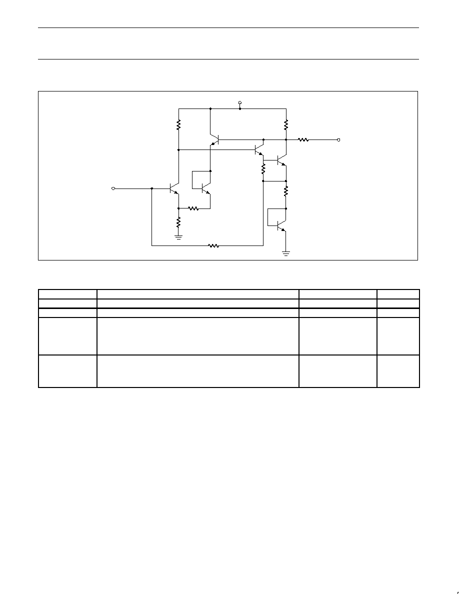
PIN CONFIGURATIONS
8
7
6
5
4
3
2
1
VCC
VIN
GND
GND
VCC
VOUT
GND
GND
N, D Packages
TOP VIEW
20dB
SR00215
Figure 1. Pin Configuration
FEATURES
∑
600MHz bandwidth
∑
20dB insertion gain
∑
4.8dB (6dB) noise figure ZO=75
(ZO=50
)
∑
No external components required
∑
Input and output impedances matched to 50/75
systems
∑
Surface mount package available
∑
MIL-STD processing available
∑
2000V ESD protection
APPLICATIONS
∑
75
cable TV decoder boxes
∑
Antenna amplifiers
∑
Amplified splitters
∑
Signal generators
∑
Frequency counters
∑
Oscilloscopes
∑
Signal analyzers
∑
Broad-band LANs
∑
Fiber-optics
∑
Modems
∑
Mobile radio
∑
Security systems
∑
Telecommunications
ORDERING INFORMATION
DESCRIPTION
TEMPERATURE RANGE
ORDER CODE
DWG #
8-Pin Plastic Small Outline (SO) package
0 to +70
∞
C
NE5205AD
SOT96-1
8-Pin Plastic Dual In-Line Package (DIP)
0 to +70
∞
C
NE5205AN
SOT97-1
8-Pin Plastic Small Outline (SO) package
-40 to +85
∞
C
SA5205AD
SOT96-1
8-Pin Plastic Dual In-Line Package (DIP)
-40 to +85
∞
C
SA5205AN
SOT97-1
8-Pin Plastic Dual In-Line Package (DIP)
-55 to +125
∞
C
SE5205AN
SOT97-1
Philips Semiconductors
Product specification
NE/SA/SE5205A
Wide-band high-frequency amplifier
1992 Feb 24
5
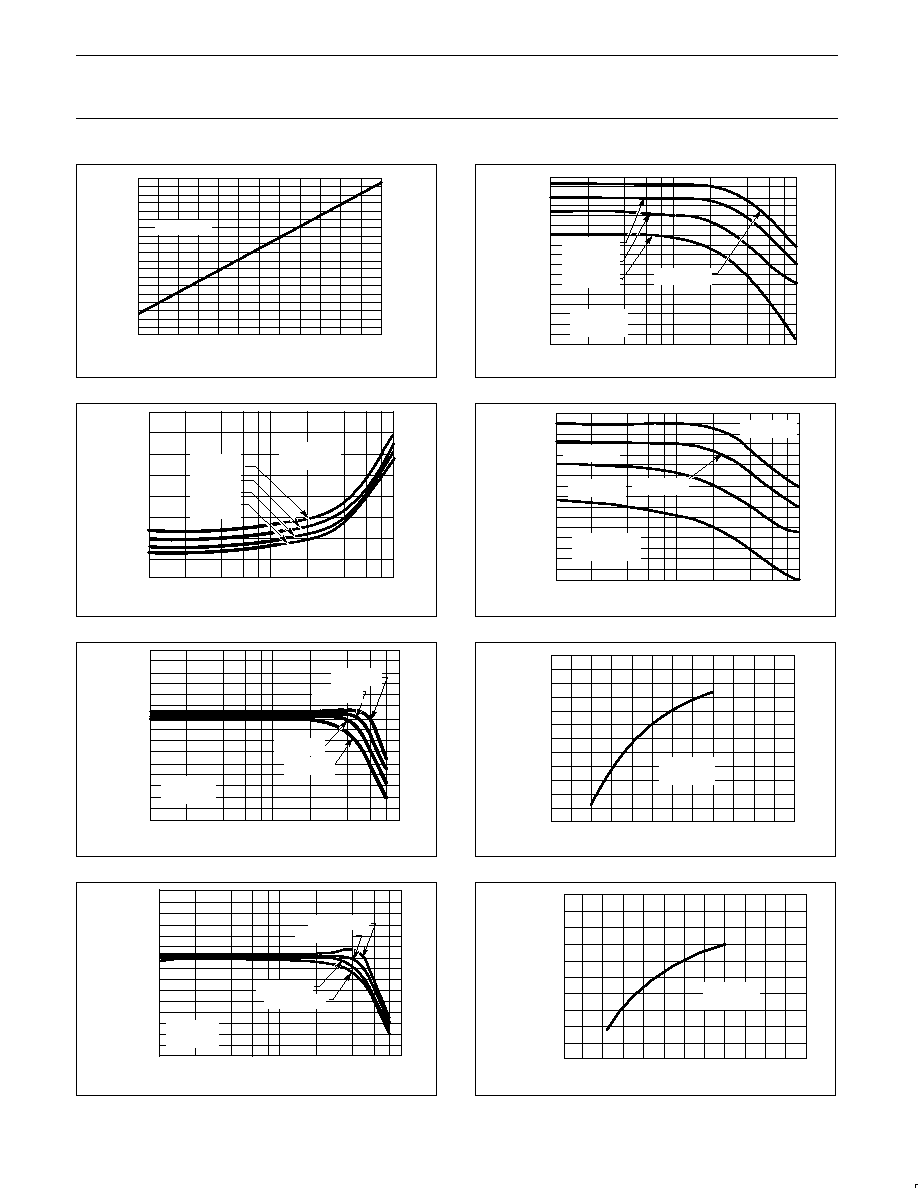
35
34
32
30
28
26
24
22
20
18
16
5
5.5
6
6.5
7
7.5
8
SUPPLY VOLTAGE--V
SUPPL
Y
CURRENT--mA
TA = 25
o
C
SR00217
Figure 3. Supply Current vs Supply Voltage
NOISE FIGURE--dBm
vcc = 6v
vcc = 8v
vcc = 7v
vcc = 5v
9
8
7
6
5
ZO = 50
TA = 25
o
C
FREQUENCY--MHz
101
2
4
6
8
2
4
6
8
102
103
SR00219
Figure 4. Noise Figure vs Frequency
INSERTION GAIN--dB
25
20
15
10
101
2
4
6
8
2
4
6
8
102
103
vcc = 8v
vcc = 7v
vcc = 6v
vcc = 5v
FREQUENCY--MHz
ZO = 50
TA = 25
o
C
SR00221
Figure 5. Insertion Gain vs Frequency (S
21
)
INSERTION GAIN--dB
TA = 55
o
C
TA = 25
o
C
TA = 85
o
C
TA = 125
o
C
VCC = 8V
ZO = 50
25
20
15
10
101
2
4
6
8
2
4
6
8
102
103
FREQUENCY--MHz
SR00223
Figure 6. Insertion Gain vs Frequency (S
21
)
OUTPUT LEVEL--dBm
FREQUENCY--MHz
ZO = 50
TA = 25
o
C
VCC = 8V
VCC = 7V
VCC = 6V
VCC = 5V
2
3
4
5
6
7
8
9
10
11
1
0
≠1
≠2
≠3
≠4
≠5
≠6
101
2
4
6
8
2
4
6
8
102
103
SR00218
Figure 7. Saturated Output Power vs Frequency
OUTPUT LEVEL--dBm
VCC = 8V
VCC = 7V
VCC = 6V
VCC = 5V
ZO = 50
TA = 25
o
C
10
9
8
7
6
5
4
3
2
1
0
≠1
≠2
≠3
≠4
≠5
≠6
FREQUENCY--MHz
101
2
4
6
8
2
4
6
8
102
103
SR00220
Figure 8. 1dB Gain Compression vs Frequency
40
35
30
25
20
15
10
4
5
6
7
8
9
10
POWER SUPPLY VOLTAGE--V
SECOND≠ORDER INTERCEPT--dBM
ZO = 50
TA = 25
o
C
SR00222
Figure 9. Second-Order Output Intercept vs Supply Voltage
30
25
20
15
10
5
4
5
6
7
8
9
10
POWER SUPPLY VOLTAGE--V
THIRD≠ORDER INTERCEPT--dBm
ZO = 50
TA = 25
o
C
SR00224
Figure 10. Third-Order Intercept vs Supply Voltage