 | –≠–ª–µ–∫—Ç—Ä–æ–Ω–Ω—ã–π –∫–æ–º–ø–æ–Ω–µ–Ω—Ç: SC16C752B | –°–∫–∞—á–∞—Ç—å:  PDF PDF  ZIP ZIP |

SC16C752B
5 V, 3.3 V and 2.5 V dual UART, 5 Mbit/s (max.), with
64-byte FIFOs
Rev. 03 -- 14 December 2004
Product data
1.
Description
The SC16C752B is a dual universal asynchronous receiver/transmitter (UART) with
64-byte FIFOs, automatic hardware/software flow control, and data rates up to
5 Mbit/s (3.3 V and 5 V). The SC16C752B offers enhanced features. It has a
transmission control register (TCR) that stores receiver FIFO threshold levels to
start/stop transmission during hardware and software flow control. With the FIFO
RDY register, the software gets the status of TXRDY/RXRDY for all four ports in one
access. On-chip status registers provide the user with error indications, operational
status, and modem interface control. System interrupts may be tailored to meet user
requirements. An internal loop-back capability allows on-board diagnostics.
The UART transmits data, sent to it over the peripheral 8-bit bus, on the TX signal and
receives characters on the RX signal. Characters can be programmed to be 5, 6, 7, or
8 bits. The UART has a 64-byte receive FIFO and transmit FIFO and can be
programmed to interrupt at different trigger levels. The UART generates its own
desired baud rate based upon a programmable divisor and its input clock. It can
transmit even, odd, or no parity and 1, 1.5, or 2 stop bits. The receiver can detect
break, idle, or framing errors, FIFO overflow, and parity errors. The transmitter can
detect FIFO underflow. The UART also contains a software interface for modem
control operations, and has software flow control and hardware flow control
capabilities.
The SC16C752B is available in plastic LQFP48 and HVQFN32 packages.
2.
Features
s
Dual channel
s
Pin compatible with SC16C2550 with additional enhancements
s
Up to 5 Mbit/s baud rate (at 3.3 V and 5 V; at 2.5 V maximum baud rate is
3 Mbit/s)
s
64-byte transmit FIFO
s
64-byte receive FIFO with error flags
s
Programmable and selectable transmit and receive FIFO trigger levels for DMA
and interrupt generation
s
Software/hardware flow control
x
Programmable Xon/Xoff characters
x
Programmable auto-RTS and auto-CTS
s
Optional data flow resume by Xon any character
s
DMA signalling capability for both received and transmitted data
s
Supports 5 V, 3.3 V and 2.5 V operation
s
5 V tolerant inputs

Philips Semiconductors
SC16C752B
5 V, 3.3 V and 2.5 V dual UART, 5 Mbit/s (max.), with 64-byte FIFOs
Product data
Rev. 03 -- 14 December 2004
2 of 47
9397 750 14443
© Koninklijke Philips Electronics N.V. 2004. All rights reserved.
s
Software selectable baud rate generator
s
Prescaler provides additional divide-by-4 function
s
Industrial temperature range (
-
40
∞
C to +85
∞
C)
s
Pin and software compatible with SC16C752, TL16C752
s
Fast databus access time
s
Programmable sleep mode
s
Programmable serial interface characteristics
x
5, 6, 7, or 8-bit characters
x
Even, odd, or no parity bit generation and detection
x
1, 1.5, or 2 stop bit generation
s
False start bit detection
s
Complete status reporting capabilities in both normal and sleep mode
s
Line break generation and detection
s
Internal test and loop-back capabilities
s
Fully prioritized interrupt system controls
s
Modem control functions (CTS, RTS, DSR, DTR, RI, and CD).
3.
Ordering information
Table 1:
Ordering information
Type number
Package
Name
Description
Version
SC16C752BIB48
LQFP48
plastic low profile quad flat package; 48 leads; body 7
◊
7
◊
1.4 mm
SOT313-2
SC16C752BIBS
HVQFN32
plastic thermal enhanced very thin quad flat package; no leads;
32 terminals; body 5
◊
5
◊
0.85 mm
SOT617-1
Philips Semiconductors
SC16C752B
5 V, 3.3 V and 2.5 V dual UART, 5 Mbit/s (max.), with 64-byte FIFOs
Product data
Rev. 03 -- 14 December 2004
3 of 47
9397 750 14443
© Koninklijke Philips Electronics N.V. 2004. All rights reserved.
4.
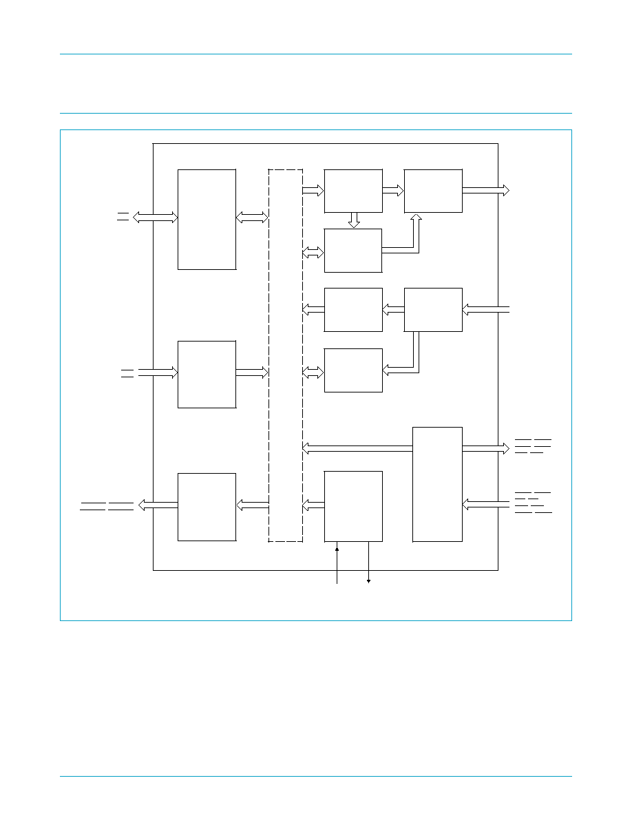
Block diagram
Fig 1.
Block diagram.
TRANSMIT
FIFO
REGISTER
TXA, TXB
RECEIVE
SHIFT
REGISTER
RECEIVE
FIFO
REGISTER
RXA, RXB
INTERCONNECT B
US LINES
AND
CONTR
OL SIGNALS
SC16C752B
TRANSMIT
SHIFT
REGISTER
MODEM
CONTROL
LOGIC
DTRA, DTRB
RTSA, RTSB
OPA, OPB
CLOCK AND
BAUD RATE
GENERATOR
CTSA, CTSB
RIA, RIB
CDA, CDB
DSRA, DSRB
XTAL2
XTAL1
DATA BUS
AND
CONTROL LOGIC
D0≠D7
IOR
IOW
RESET
A0≠A2
CSA
CSB
REGISTER
SELECT
LOGIC
INTA, INTB
TXRDYA , TXRDYB
RXRDYA , RXRDYB
INTERRUPT
CONTROL
LOGIC
002aaa600
FLOW
CONTROL
LOGIC
FLOW
CONTROL
LOGIC
Philips Semiconductors
SC16C752B
5 V, 3.3 V and 2.5 V dual UART, 5 Mbit/s (max.), with 64-byte FIFOs
Product data
Rev. 03 -- 14 December 2004
4 of 47
9397 750 14443
© Koninklijke Philips Electronics N.V. 2004. All rights reserved.
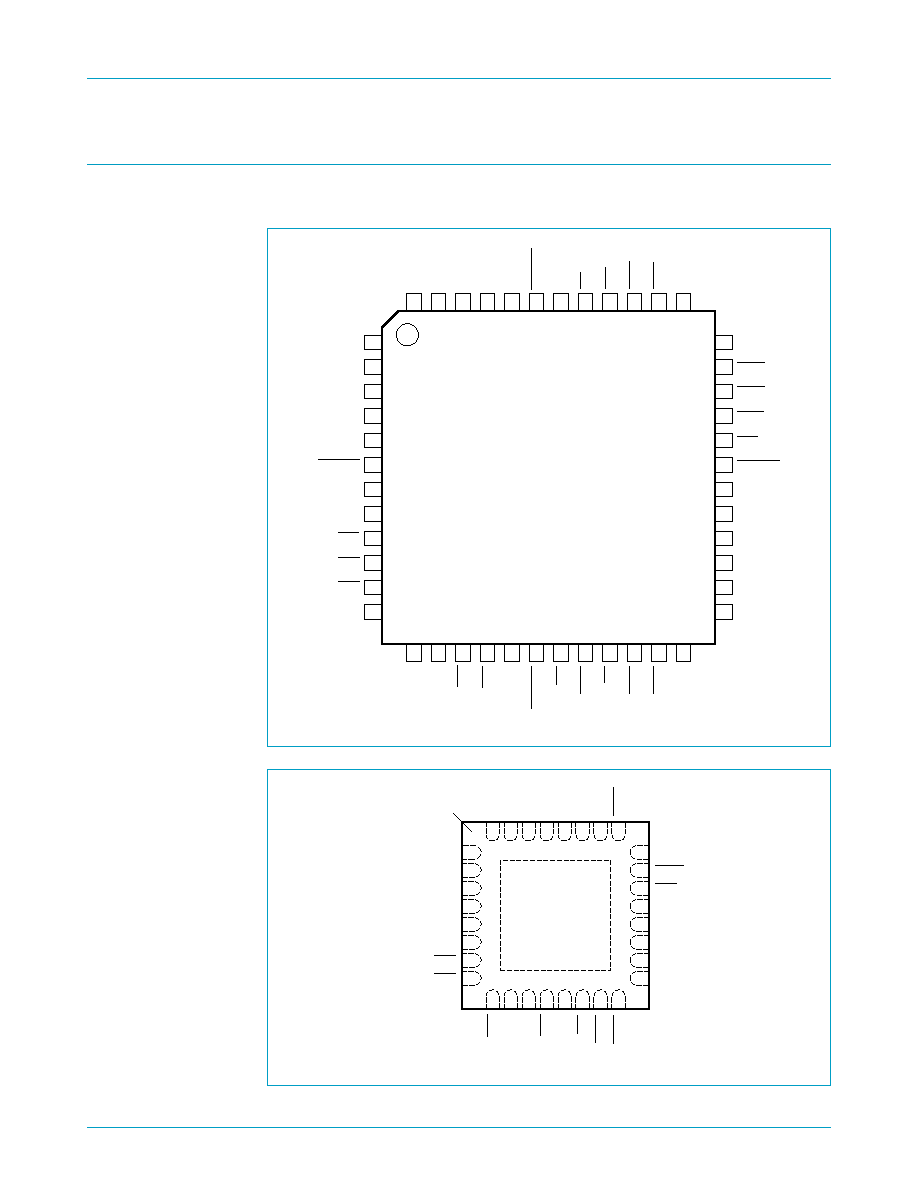
5.
Pinning information
5.1 Pinning
Fig 2.
LQFP48 pin configuration.
Fig 3.
HVQFN32 pin configuration.
SC16C752BIB48
002aaa601
1
2
3
4
5
6
7
8
9
10
11
12
36
35
34
33
32
31
30
29
28
27
26
25
13
14
15
16
17
18
19
20
21
22
23
24
48
47
46
45
44
43
42
41
40
39
38
37
D4
D3
D2
D1
D0
TXRDYA
V
CC
RIA
CDA
DSRA
CTSA
n.c.
XTAL1
XTAL2
IOW
CDB
GND
RXRDYB
IOR
DSRB
RIB
RTSB
CTSB
n.c.
D5
D6
D7
RXB
RXA
TXRDYB
TXA
TXB
OPB
CSA
CSB
n.c.
RESET
DTRB
DTRA
RTSA
OPA
RXRDYA
INTA
INTB
A0
A1
A2
n.c.
002aaa950
SC16C752BIBS
(top view)
A2
OPB
CSA
A1
TXB
TXA
INTB
RXA
INTA
RXB
OPA
D7
RTSA
D6
RESET
CSB
XTAL1
IOW
GND
IOR
RTSB
CTSB
D5
D4
D3
D2
D1
D0
V
CC
CTSA
8
17
7
18
6
19
5
20
4
21
3
22
2
23
1
24
9
10
11
12
13
14
15
16
32
31
30
29
28
27
26
25
terminal 1
index area
XTAL2
A0

Philips Semiconductors
SC16C752B
5 V, 3.3 V and 2.5 V dual UART, 5 Mbit/s (max.), with 64-byte FIFOs
Product data
Rev. 03 -- 14 December 2004
5 of 47
9397 750 14443
© Koninklijke Philips Electronics N.V. 2004. All rights reserved.
5.2 Pin description
Table 2:
Pin description
Symbol
Pin
Type
Description
LQFP48 HVQFN32
A0
28
19
I
Address 0 select bit. Internal registers address selection.
A1
27
18
I
Address 1 select bit. Internal registers address selection.
A2
26
17
I
Address 2 select bit. Internal registers address selection.
CDA, CDB
40, 16
-
I
Carrier Detect (Active-LOW). These inputs are associated with individual
UART channels A and B. A logic LOW on these pins indicates that a carrier
has been detected by the modem for that channel. The state of these inputs
is reflected in the modem status register (MSR).
CSA, CSB
10, 11
8, 9
I
Chip Select (Active-LOW). These pins enable data transfers between the
user CPU and the SC16C752B for the channel(s) addressed. Individual
UART sections (A, B) are addressed by providing a logic LOW on the
respective CSA and CSB pins.
CTSA,
CTSB
38, 23
25, 16
I
Clear to Send (Active-LOW). These inputs are associated with individual
UART channels A and B. A logic 0 (LOW) on the CTS pins indicates the
modem or data set is ready to accept transmit data from the SC16C752B.
Status can be tested by reading MSR[4]. These pins only affect the transmit
and receive operations when Auto-CTS function is enabled via the Enhanced
Feature Register EFR[7] for hardware flow control operation.
D0-D4,
D5-D7
44-48,
1-3
27-31, 32,
1-2
I/O
Data bus (bi-directional). These pins are the 8-bit, 3-state data bus for
transferring information to or from the controlling CPU. D0 is the least
significant bit and the first data bit in a transmit or receive serial data stream.
DSRA,
DSRB
39, 20
-
I
Data Set Ready (Active-LOW). These inputs are associated with individual
UART channels A and B. A logic 0 (LOW) on these pins indicates the modem
or data set is powered-on and is ready for data exchange with the UART. The
state of these inputs is reflected in the modem status register (MSR).
DTRA,
DTRB
34, 35
-
O
Data Terminal Ready (Active-LOW). These outputs are associated with
individual UART channels A and B. A logic 0 (LOW) on these pins indicates
that the SC16C752B is powered-on and ready. These pins can be controlled
via the modem control register. Writing a logic 1 to MCR[0] will set the DTR
output to logic 0 (LOW), enabling the modem. The output of these pins will
be a logic 1 after writing a logic 0 to MCR[0], or after a reset.
GND
17
13
I
Signal and power ground.
INTA, INTB
30, 29
21, 20
O
Interrupt A and B (Active-HIGH). These pins provide individual channel
interrupts INTA and INTB. INTA and INTB are enabled when MCR[3] is set to
a logic 1, interrupt sources are enabled in the interrupt enable register (IER).
Interrupt conditions include: receiver errors, available receiver buffer data,
available transmit buffer space, or when a modem status flag is detected.
INTA, INTB are in the high-impedance state after reset.
IOR
19
14
I
Input/Output Read strobe (Active-LOW). A HIGH-to-LOW transition on
IOR will load the contents of an internal register defined by address bits
A0-A2 onto the SC16C752B data bus (D0-D7) for access by external CPU.
IOW
15
12
I
Input/Output Write strobe (Active-LOW). A LOW-to-HIGH transition on
IOW will transfer the contents of the data bus (D0-D7) from the external CPU
to an internal register that is defined by address bits A0-A2 and CSA and
CSB.
n.c.
12, 24,
25, 37
-
-
Not connected.

Philips Semiconductors
SC16C752B
5 V, 3.3 V and 2.5 V dual UART, 5 Mbit/s (max.), with 64-byte FIFOs
Product data
Rev. 03 -- 14 December 2004
6 of 47
9397 750 14443
© Koninklijke Philips Electronics N.V. 2004. All rights reserved.
OPA, OPB
32, 9
22, 7
O
User defined outputs. This function is associated with individual channels A
and B. The state of these pins is defined by the user through the software
settings of MCR[3]. INTA-INTB are set to active mode and OPA-OPB to a
logic 0 when MCR[3] is set to a logic 1. INTA-INTB are set to the 3-State
mode and OPA-OPB to a logic 1 when MCR[3] is set to a logic 0. The output
of these two pins is HIGH after reset.
RESET
36
24
I
Reset. This pin will reset the internal registers and all the outputs. The UART
transmitter output and the receiver input will be disabled during reset time.
RESET is an active-HIGH input.
RIA, RIB
41, 21
-
I
Ring Indicator (Active-LOW). These inputs are associated with individual
UART channels, A and B. A logic 0 on these pins indicates the modem has
received a ringing signal from the telephone line. A LOW-to-HIGH transition
on these input pins generates a modem status interrupt, if enabled. The state
of these inputs is reflected in the modem status register (MSR).
RTSA,
RTSB
33, 22
23, 15
O
Request to Send (Active-LOW). These outputs are associated with
individual UART channels, A and B. A logic 0 on the RTS pin indicates the
transmitter has data ready and waiting to send. Writing a logic 1 in the
modem control register MCR[1] will set this pin to a logic 0, indicating data is
available. After a reset these pins are set to a logic 1. These pins only affect
the transmit and receive operations when Auto-RTS function is enabled via
the Enhanced Feature Register (EFR[6]) for hardware flow control operation.
RXA, RXB
5, 4
4, 3
I
Receive data input. These inputs are associated with individual serial
channel data to the SC16C752B. During the local loop-back mode, these RX
input pins are disabled and TX data is connected to the UART RX input
internally.
RXRDYA,
RXRDYB
31, 18
-
O
Receive Ready (Active-LOW). RXRDYA or RXRDYB goes LOW when the
trigger level has been reached or the FIFO has at least one character. It goes
HIGH when the RX FIFO is empty.
TXA, TXB
7, 8
5, 6
O
Transmit data A, B. These outputs are associated with individual serial
transmit channel data from the SC16C752B. During the local loop-back
mode, the TX output pin is disabled and TX data is internally connected to
the UART RX input.
TXRDYA,
TXRDYB
43, 6
-
O
Transmit Ready (Active-LOW). TXRDYA or TXRDYB go LOW when there
are at least a trigger level number of spaces available or when the FIFO is
empty. It goes HIGH when the FIFO is full or not empty.
V
CC
42
26
I
Power supply input.
XTAL1
13
10
I
Crystal or external clock input. Functions as a crystal input or as an
external clock input. A crystal can be connected between XTAL1 and XTAL2
to form an internal oscillator circuit (see
Figure 13
). Alternatively, an external
clock can be connected to this pin to provide custom data rates.
XTAL2
14
11
O
Output of the crystal oscillator or buffered clock. (See also XTAL1.)
XTAL2 is used as a crystal oscillator output or a buffered clock output.
Table 2:
Pin description
...continued
Symbol
Pin
Type
Description
LQFP48 HVQFN32

Philips Semiconductors
SC16C752B
5 V, 3.3 V and 2.5 V dual UART, 5 Mbit/s (max.), with 64-byte FIFOs
Product data
Rev. 03 -- 14 December 2004
7 of 47
9397 750 14443
© Koninklijke Philips Electronics N.V. 2004. All rights reserved.
6.
Functional description
The SC16C752B UART is pin-compatible with the SC16C2550 UART. It provides
more enhanced features. All additional features are provided through a special
enhanced feature register.
The UART will perform serial-to-parallel conversion on data characters received from
peripheral devices or modems, and parallel-to-parallel conversion on data characters
transmitted by the processor. The complete status of each channel of the
SC16C752B UART can be read at any time during functional operation by the
processor.
The SC16C752B can be placed in an alternate mode (FIFO mode) relieving the
processor of excessive software overhead by buffering received/transmitted
characters. Both the receiver and transmitter FIFOs can store up to 64 bytes
(including three additional bits of error status per byte for the receiver FIFO) and have
selectable or programmable trigger levels. Primary outputs RXRDY and TXRDY allow
signalling of DMA transfers.
The SC16C752B has selectable hardware flow control and software flow control.
Hardware flow control significantly reduces software overhead and increases system
efficiency by automatically controlling serial data flow using the RTS output and CTS
input signals. Software flow control automatically controls data flow by using
programmable Xon/Xoff characters.
The UART includes a programmable baud rate generator that can divide the timing
reference clock input by a divisor between 1 and (2
16
-
1).
6.1 Trigger levels
The SC16C752B provides independent selectable and programmable trigger levels
for both receiver and transmitter DMA and interrupt generation. After reset, both
transmitter and receiver FIFOs are disabled and so, in effect, the trigger level is the
default value of one byte. The selectable trigger levels are available via the FCR. The
programmable trigger levels are available via the TLR.
6.2 Hardware flow control
Hardware flow control is comprised of Auto-CTS and Auto-RTS. Auto-CTS and
Auto-RTS can be enabled/disabled independently by programming EFR[7:6].
With Auto-CTS, CTS must be active before the UART can transmit data.
Auto-RTS only activates the RTS output when there is enough room in the FIFO to
receive data and de-activates the RTS output when the RX FIFO is sufficiently full.
The halt and resume trigger levels in the TCR determine the levels at which RTS is
activated/deactivated.
If both Auto-CTS and Auto-RTS are enabled, when RTS is connected to CTS, data
transmission does not occur unless the receiver FIFO has empty space. Thus,
overrun errors are eliminated during hardware flow control. If not enabled, overrun
errors occur if the transmit data rate exceeds the receive FIFO servicing latency.

Philips Semiconductors
SC16C752B
5 V, 3.3 V and 2.5 V dual UART, 5 Mbit/s (max.), with 64-byte FIFOs
Product data
Rev. 03 -- 14 December 2004
8 of 47
9397 750 14443
© Koninklijke Philips Electronics N.V. 2004. All rights reserved.
6.2.1
Auto-RTS
Auto-RTS data flow control originates in the receiver block (see
Figure 1 "Block
diagram." on page 3
).
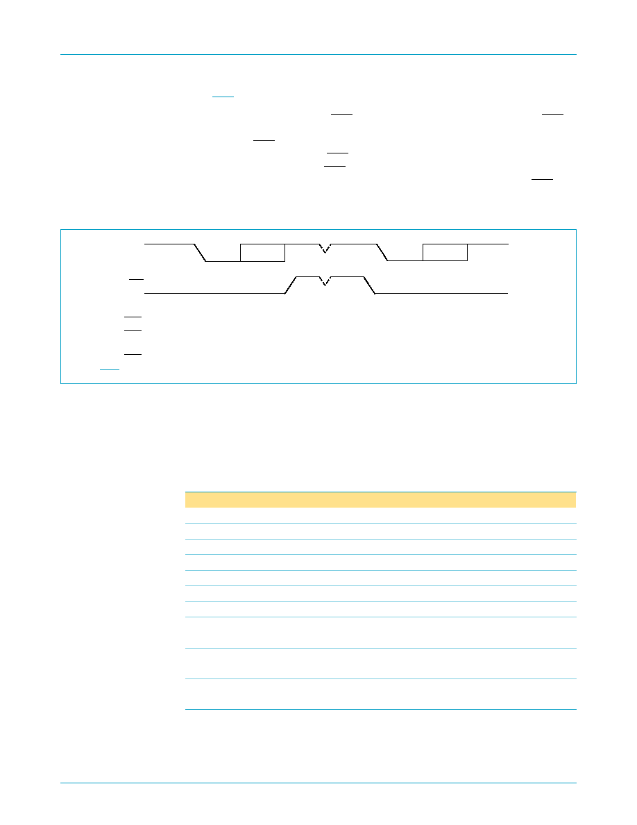
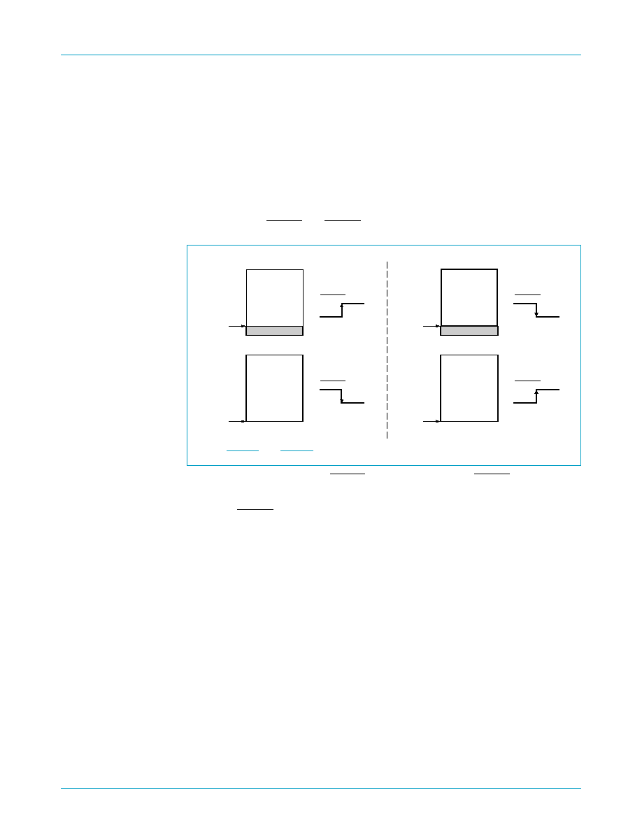
Figure 5
shows RTS functional timing. The receiver FIFO
trigger levels used in Auto-RTS are stored in the TCR. RTS is active if the RX FIFO
level is below the halt trigger level in TCR[3:0]. When the receiver FIFO halt trigger
level is reached, RTS is deasserted. The sending device (e.g., another UART) may
send an additional byte after the trigger level is reached (assuming the sending UART
has another byte to send) because it may not recognize the deassertion of RTS until
it has begun sending the additional byte. RTS is automatically reasserted once the
receiver FIFO reaches the resume trigger level programmed via TCR[7:4]. This
reassertion allows the sending device to resume transmission.
Fig 4.
Autoflow control (Auto-RTS and Auto-CTS) example.
RX
FIFO
FLOW
CONTROL
TX
FIFO
PARALLEL
TO SERIAL
TX
FIFO
RX
FIFO
UART 1
UART 2
D7 to D0
RX
TX
RTS
CTS
TX
RX
CTS
RTS
D7 to D0
002aaa228
SERIAL TO
PARALLEL
SERIAL TO
PARALLEL
FLOW
CONTROL
FLOW
CONTROL
FLOW
CONTROL
PARALLEL
TO SERIAL
(1) N = receiver FIFO trigger level.
(2) The two blocks in dashed lines cover the case where an additional byte is sent, as described in
Section 6.2.1
.
Fig 5.
RTS functional timing.
Start
byte N
Start
byte N
+
1
Start
Stop
Stop
RX
RTS
IOR
N
N+1
1
2
002aaa226
Philips Semiconductors
SC16C752B
5 V, 3.3 V and 2.5 V dual UART, 5 Mbit/s (max.), with 64-byte FIFOs
Product data
Rev. 03 -- 14 December 2004
9 of 47
9397 750 14443
© Koninklijke Philips Electronics N.V. 2004. All rights reserved.
6.2.2
Auto-CTS
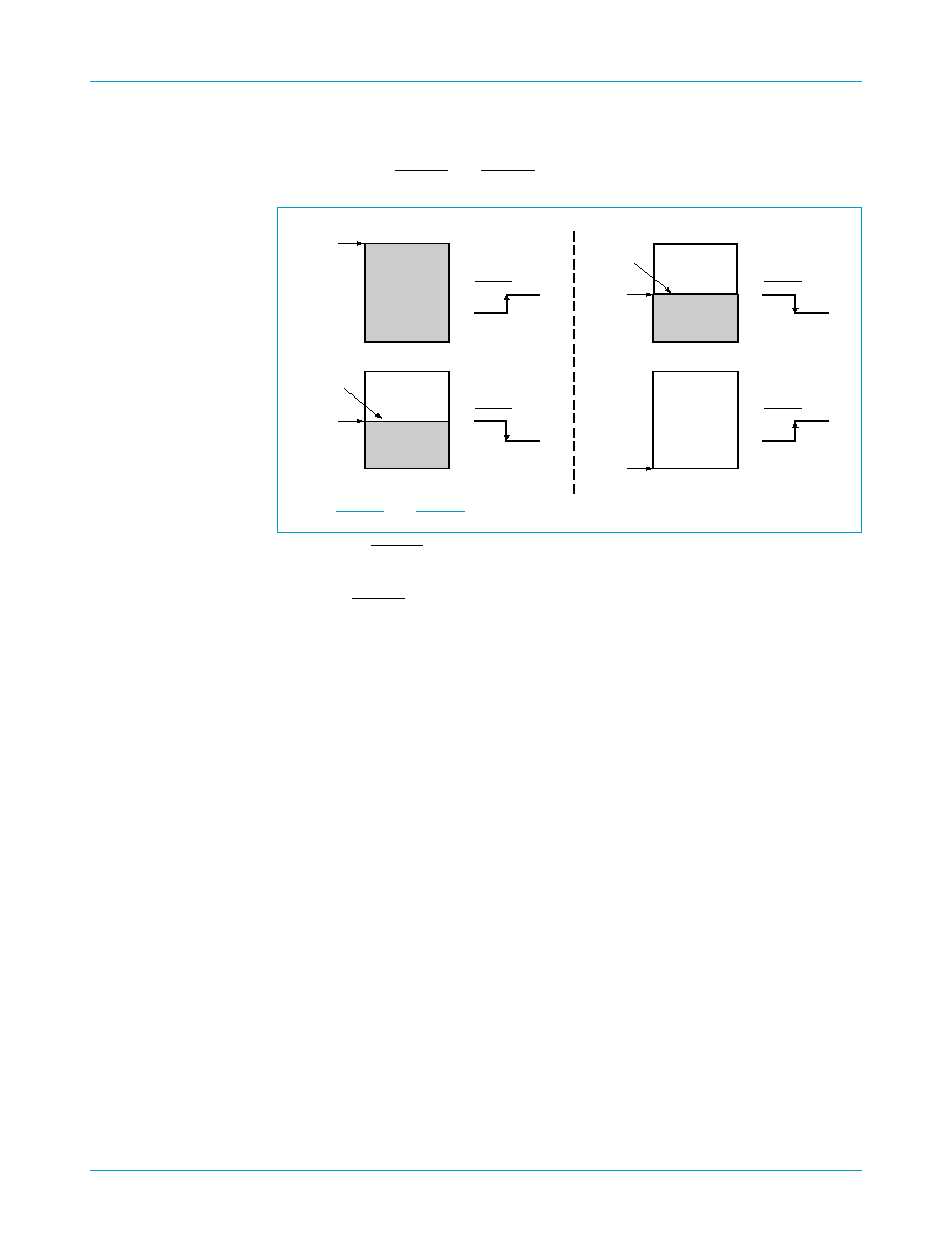
The transmitter circuitry checks CTS before sending the next data byte. When CTS is
active, the transmitter sends the next byte. To stop the transmitter from sending the
following byte, CTS must be deasserted before the middle of the last stop bit that is
currently being sent. The auto-CTS function reduces interrupts to the host system.
When flow control is enabled, CTS level changes do not trigger host interrupts
because the device automatically controls its own transmitter. Without auto-CTS, the
transmitter sends any data present in the transmit FIFO and a receiver overrun error
may result.
6.3 Software flow control
Software flow control is enabled through the enhanced feature register and the
modem control register. Different combinations of software flow control can be
enabled by setting different combinations of EFR[3:0].
Table 3
shows software flow
control options.
(1) When CTS is LOW, the transmitter keeps sending serial data out.
(2) When CTS goes HIGH before the middle of the last stop bit of the current byte, the transmitter finishes sending the current
byte, but is does not send the next byte.
(3) When CTS goes from HIGH to LOW, the transmitter begins sending data again.
Fig 6.
CTS functional timing.
Start
byte 0 to 7
Stop
TX
CTS
002aaa227
Start
byte 0 to 7
Stop
Table 3:
Software flow control options (EFR[0:3])
EFR[3]
EFR[2]
EFR[1]
EFR[0]
TX, RX software flow controls
0
0
X
X
no transmit flow control
1
0
X
X
transmit Xon1, Xoff1
0
1
X
X
transmit Xon2, Xoff2
1
1
X
X
transmit Xon1, Xon2, Xoff1, Xoff2
X
X
0
0
no receive flow control
X
X
1
0
receiver compared Xon1, Xoff1
X
X
0
1
receiver compares Xon2, Xoff2
1
0
1
1
transmit Xon1, Xoff1
receiver compares Xon1 and Xon2, Xoff1 and Xoff2
0
1
1
1
transmit Xon2, Xoff2
receiver compares Xon1 and Xon2, Xoff1 and Xoff2
1
1
1
1
transmit Xon1, Xon2, Xoff1, Xoff2
receiver compares Xon1 and Xon2, Xoff1 and Xoff2

Philips Semiconductors
SC16C752B
5 V, 3.3 V and 2.5 V dual UART, 5 Mbit/s (max.), with 64-byte FIFOs
Product data
Rev. 03 -- 14 December 2004
10 of 47
9397 750 14443
© Koninklijke Philips Electronics N.V. 2004. All rights reserved.
There are two other enhanced features relating to software flow control:
∑
Xon Any function (MCR[5]): Operation will resume after receiving any character
after recognizing the Xoff character. It is possible that an Xon1 character is
recognized as an Xon Any character, which could cause an Xon2 character to be
written to the RX FIFO.
∑
Special character (EFR[5]): Incoming data is compared to Xoff2. Detection of the
special character sets the Xoff interrupt (IIR[4]) but does not halt transmission. The
Xoff interrupt is cleared by a read of the IIR. The special character is transferred to
the RX FIFO.
6.3.1
RX
When software flow control operation is enabled, the SC16C752B will compare
incoming data with Xoff1,2 programmed characters (in certain cases, Xoff1 and Xoff2
must be received sequentially). When the correct Xoff character are received,
transmission is halted after completing transmission of the current character. Xoff
detection also sets IIR[4] (if enabled via IER[5]) and causes INT to go HIGH.
To resume transmission, an Xon1,2 character must be received (in certain cases
Xon1 and Xon2 must be received sequentially). When the correct Xon characters are
received, IIR[4] is cleared, and the Xoff interrupt disappears.
6.3.2
TX
Xoff1/2 character is transmitted when the RX FIFO has passed the HALT trigger level
programmed in TCR[3:0].
Xon1/2 character is transmitted when the RX FIFO reaches the RESUME trigger
level programmed in TCR[7:4].
The transmission of Xoff/Xon(s) follows the exact same protocol as transmission of
an ordinary byte from the FIFO. This means that even if the word length is set to be 5,
6, or 7 characters, then the 5, 6, or 7 least significant bits of Xoff1,2/Xon1,2 will be
transmitted. (Note that the transmission of 5, 6, or 7 bits of a character is seldom
done, but this functionality is included to maintain compatibility with earlier designs.)
It is assumed that software flow control and hardware flow control will never be
enabled simultaneously.
Figure 7
shows an example of software flow control.
Philips Semiconductors
SC16C752B
5 V, 3.3 V and 2.5 V dual UART, 5 Mbit/s (max.), with 64-byte FIFOs
Product data
Rev. 03 -- 14 December 2004
11 of 47
9397 750 14443
© Koninklijke Philips Electronics N.V. 2004. All rights reserved.
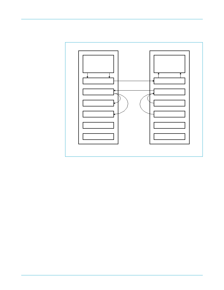
6.3.3
Software flow control example
Assumptions:
UART1 is transmitting a large text file to UART2. Both UARTs are
using software flow control with single character Xoff (0F) and Xon (0D) tokens. Both
have Xoff threshold (TCR[3:0] = F) set to 60, and Xon threshold (TCR[7:4] = 8) set to
32. Both have the interrupt receive threshold (TLR[7:4] = D) set to 52.
UART 1 begins transmission and sends 52 characters, at which point UART2 will
generate an interrupt to its processor to service the RCV FIFO, but assume the
interrupt latency is fairly long. UART1 will continue sending characters until a total of
60 characters have been sent. At this time, UART2 will transmit a 0F to UART1,
informing UART1 to halt transmission. UART1 will likely send the 61
st
character while
UART2 is sending the Xoff character. Now UART2 is serviced and the processor
reads enough data out of the RX FIFO that the level drops to 32. UART2 will now
send a 0D to UART1, informing UART1 to resume transmission.
Fig 7.
Software flow control example.
TRANSMIT FIFO
PARALLEL-TO-SERIAL
SERIAL-TO-PARALLEL
Xon-1 WORD
Xon-2 WORD
Xoff-1 WORD
Xoff-2 WORD
RECEIVE FIFO
PARALLEL-TO-SERIAL
SERIAL-TO-PARALLEL
Xon-1 WORD
Xon-2 WORD
Xoff-1 WORD
Xoff-2 WORD
UART2
UART1
002aaa229
data
Xoff≠Xon≠Xoff
compare
programmed
Xon-Xoff
characters

Philips Semiconductors
SC16C752B
5 V, 3.3 V and 2.5 V dual UART, 5 Mbit/s (max.), with 64-byte FIFOs
Product data
Rev. 03 -- 14 December 2004
12 of 47
9397 750 14443
© Koninklijke Philips Electronics N.V. 2004. All rights reserved.
6.4 Reset
Table 4
summarizes the state of register after reset.
[1]
Registers DLL, DLH, SPR, Xon1, Xon2, Xoff1, Xoff2 are not reset by the top-level reset signal
RESET, i.e., they hold their initialization values during reset.
Table 5
summarizes the state of registers after reset.
Table 4:
Register reset functions
Register
Reset control
Reset state
Interrupt enable register
RESET
All bits cleared.
Interrupt identification register
RESET
Bit 0 is set. All other bits cleared.
FIFO control register
RESET
All bits cleared.
Line control register
RESET
Reset to 00011101 (1D hex).
Modem control register
RESET
All bits cleared.
Line status register
RESET
Bits 5 and 6 set. All other bits cleared.
Modem status register
RESET
Bits 0-3 cleared. Bits 4-7 input signals.
Enhanced feature register
RESET
All bits cleared.
Receiver holding register
RESET
Pointer logic cleared.
Transmitter holding register
RESET
Pointer logic cleared.
Transmission control register
RESET
All bits cleared.
Trigger level register
RESET
All bits cleared.
Table 5:
Signal RESET functions
Signal
Reset control
Reset state
TX
RESET
high
RTS
RESET
high
DTR
RESET
high
RXRDY
RESET
high
TXRDY
RESET
low

Philips Semiconductors
SC16C752B
5 V, 3.3 V and 2.5 V dual UART, 5 Mbit/s (max.), with 64-byte FIFOs
Product data
Rev. 03 -- 14 December 2004
13 of 47
9397 750 14443
© Koninklijke Philips Electronics N.V. 2004. All rights reserved.
6.5 Interrupts
The SC16C752B has interrupt generation and prioritization (six prioritized levels of
interrupts) capability. The interrupt enable register (IER) enables each of the six types
of interrupts and the INT signal in response to an interrupt generation. The IER can
also disable the interrupt system by clearing bits 0-3, 5-7. When an interrupt is
generated, the IIR indicates that an interrupt is pending and provides the type of
interrupt through IIR[5;0].
Table 6
summarizes the interrupt control functions.
It is important to note that for the framing error, parity error, and break conditions,
LSR[7] generates the interrupt. LSR[7] is set when there is an error anywhere in the
RX FIFO, and is cleared only when there are no more errors remaining in the FIFO.
LSR[4:2] always represent the error status for the received character at the top of the
RX FIFO. Reading the RX FIFO updates LSR[4:2] to the appropriate status for the
new character at the top of the FIFO. If the RX FIFO is empty, then LSR[4:2] are all
zeros.
For the Xoff interrupt, if an Xoff flow character detection caused the interrupt, the
interrupt is cleared by an Xon flow character detection. If a special character
detection caused the interrupt, the interrupt is cleared by a read of the LSR.
Table 6:
Interrupt control functions
IIR[5:0]
Priority
level
Interrupt type
Interrupt source
Interrupt reset method
000001
None
none
none
none
000110
1
receiver line status
OE, FE, PE, or BI errors occur in
characters in the RX FIFO
FE, PE, BI: all erroneous
characters are read from the
RX FIFO.
OE: read LSR
001100
2
RX time-out
stale data in RX FIFO
read RHR
000100
2
RHR interrupt
DRDY (data ready)
(FIFO disable)
RX FIFO above trigger level
(FIFO enable)
read RHR
000010
3
THR interrupt
TFE (THR empty)
(FIFO disable)
TX FIFO passes above trigger level
(FIFO enable)
read IIR or a write to the THR
000000
4
modem status
MSR[3:0] = 0
read MSR
010000
5
Xoff interrupt
receive Xoff character(s)/special
character
receive Xon character(s)/Read of
IIR
100000
6
CTS, RTS
RTS pin or CTS pin change state from
active (LOW) to inactive (HIGH)
read IIR

Philips Semiconductors
SC16C752B
5 V, 3.3 V and 2.5 V dual UART, 5 Mbit/s (max.), with 64-byte FIFOs
Product data
Rev. 03 -- 14 December 2004
14 of 47
9397 750 14443
© Koninklijke Philips Electronics N.V. 2004. All rights reserved.
6.5.1
Interrupt mode operation
In interrupt mode (if any bit of IER[3:0] is 1) the processor is informed of the status of
the receiver and transmitter by an interrupt signal, INT. Therefore, it is not necessary
to continuously poll the line status register (LSR) to see if any interrupt needs to be
serviced.
Figure 8
shows interrupt mode operation.
6.5.2
Polled mode operation
In polled mode (IER[3:0] = 0000) the status of the receiver and transmitter can be
checked by polling the line status register (LSR). This mode is an alternative to the
FIFO interrupt mode of operation where the status of the receiver and transmitter is
automatically known by means of interrupts sent to the CPU.
Figure 9
shows FIFO
polled mode operation.
Fig 8.
Interrupt mode operation.
1
1
1
1
IIR
IER
THR
RHR
PROCESSOR
IOW / IOR
INT
002aaa230
Fig 9.
FIFO polled mode operation.
0
0
0
0
LSR
IER
THR
RHR
PROCESSOR
IOW / IOR
002aaa231
Philips Semiconductors
SC16C752B
5 V, 3.3 V and 2.5 V dual UART, 5 Mbit/s (max.), with 64-byte FIFOs
Product data
Rev. 03 -- 14 December 2004
15 of 47
9397 750 14443
© Koninklijke Philips Electronics N.V. 2004. All rights reserved.
6.6 DMA operation
There are two modes of DMA operation, DMA mode 0 or DMA mode 1, selected by
FCR[3].
In DMA mode 0 or FIFO disable (FCR[0] = 0) DMA occurs in single character
transfers. In DMA mode 1, multi-character (or block) DMA transfers are managed to
relieve the processor for longer periods of time.
6.6.1
Single DMA transfers (DMA mode 0/FIFO disable)
Figure 10
shows TXRDY and RXRDY in DMA mode 0/FIFO disable.
Transmitter:
When empty, the TXRDY signal becomes active. TXRDY will go inactive
after one character has been loaded into it.
Receiver:
RXRDY is active when there is at least one character in the FIFO. It
becomes inactive when the receiver is empty.
Fig 10. TXRDY and RXRDY in DMA mode 0/FIFO disable.
TX
wrptr
wrptr
FIFO EMPTY
TXRDY
RX
rdptr
rdptr
FIFO EMPTY
RXRDY
RXRDY
002aaa232
at least one
location filled
at least one
location filled
TXRDY
Philips Semiconductors
SC16C752B
5 V, 3.3 V and 2.5 V dual UART, 5 Mbit/s (max.), with 64-byte FIFOs
Product data
Rev. 03 -- 14 December 2004
16 of 47
9397 750 14443
© Koninklijke Philips Electronics N.V. 2004. All rights reserved.
6.6.2
Block DMA transfers (DMA mode 1)
Figure 11
shows TXRDY and RXRDY in DMA mode 1.
Transmitter:
TXRDY is active when there is a trigger level number of spaces
available. It becomes inactive when the FIFO is full.
Receiver:
RXRDY becomes active when the trigger level has been reached, or when
a time-out interrupt occurs. It will go inactive when the FIFO is empty or an error in
the RX FIFO is flagged by LSR[7].
6.7 Sleep mode
Sleep mode is an enhanced feature of the SC16C752B UART. It is enabled when
EFR[4], the enhanced functions bit, is set and when IER[4] is set. Sleep mode is
entered when:
∑
The serial data input line, RX, is idle (see
Section 6.8 "Break and time-out
conditions"
).
∑
The TX FIFO and TX shift register are empty.
∑
There are no interrupts pending except THR and time-out interrupts.
Remark: Sleep mode will not be entered if there is data in the RX FIFO.
In sleep mode, the UART clock and baud rate clock are stopped. Since most registers
are clocked using these clocks, the power consumption is greatly reduced. The UART
will wake up when any change is detected on the RX line, when there is any change
in the state of the modem input pins, or if data is written to the TX FIFO.
Remark: Writing to the divisor latches, DLL and DLH, to set the baud clock, must not
be done during sleep mode. Therefore, it is advisable to disable sleep mode using
IER[4] before writing to DLL or DLH.
Fig 11. TXRDY and RXRDY in DMA mode 1.
TX
wrptr
wrptr
TXRDY
FIFO full
TXRDY
RX
rdptr
rdptr
FIFO EMPTY
RXRDY
RXRDY
002aaa234
trigger
level
trigger
level
at least one
location filled

Philips Semiconductors
SC16C752B
5 V, 3.3 V and 2.5 V dual UART, 5 Mbit/s (max.), with 64-byte FIFOs
Product data
Rev. 03 -- 14 December 2004
17 of 47
9397 750 14443
© Koninklijke Philips Electronics N.V. 2004. All rights reserved.
6.8 Break and time-out conditions
An RX idle condition is detected when the receiver line, RX, has been HIGH for
4 character time. The receiver line is sampled midway through each bit.
When a break condition occurs, the TX line is pulled LOW. A break condition is
activated by setting LCR[6].
6.9 Programmable baud rate generator
The SC16C752B UART contains a programmable baud generator that takes any
clock input and divides it by a divisor in the range between 1 and (2
16
-
1). An
additional divide-by-4 prescaler is also available and can be selected by MCR[7], as
shown in
Figure 12
. The output frequency of the baud rate generator is 16
◊
the baud
rate. The formula for the divisor is:
Where:
prescaler = 1, when MCR[7] is set to 0 after reset (divide-by-1 clock selected)
prescaler = 4, when MCR[7] is set to 1 after reset (divide-by-4 clock selected).
Remark: The default value of prescaler after reset is divide-by-1.
Figure 12
shows the internal prescaler and baud rate generator circuitry.
DLL and DLH must be written to in order to program the baud rate. DLL and DLH are
the least significant and most significant byte of the baud rate divisor. If DLL and DLH
are both zero, the UART is effectively disabled, as no baud clock will be generated.
Remark: The programmable baud rate generator is provided to select both the
transmit and receive clock rates.
Table 7
and
Table 8
show the baud rate and divisor correlation for crystal with
frequency 1.8432 MHz and 3.072 MHz, respectively.
Figure 13
shows the crystal clock circuit reference.
Fig 12. Prescaler and baud rate generator block diagram.
divisor
XTAL1 crystal input frequency
prescaler
---------------------------------------------------------------------------
desired baud rate
16
◊
(
)
---------------------------------------------------------------------------------
=
BAUD RATE
GENERATOR
LOGIC
MCR[7] = 1
MCR[7] = 0
PRESCALER
LOGIC
(DIVIDE-BY-1)
INTERNAL
OSCILLATOR
LOGIC
002aaa233
XTAL1
XTAL2
input clock
PRESCALER
LOGIC
(DIVIDE-BY-4)
reference
clock
internal
baud rate
clock for
transmitter
and receive

Philips Semiconductors
SC16C752B
5 V, 3.3 V and 2.5 V dual UART, 5 Mbit/s (max.), with 64-byte FIFOs
Product data
Rev. 03 -- 14 December 2004
18 of 47
9397 750 14443
© Koninklijke Philips Electronics N.V. 2004. All rights reserved.
Table 7:
Baud rates using a 1.8432 MHz crystal
Desired baud rate
Divisor used to generate
16
◊
clock
Percent error difference
between desired and actual
50
2304
75
1536
110
1047
0.026
134.5
857
0.058
150
768
300
384
600
192
1200
96
1800
64
2000
58
0.69
2400
48
3600
32
4800
24
7200
16
9600
12
19200
6
38400
3
56000
2
2.86
Table 8:
Baud rates using a 3.072 MHz crystal
Desired baud rate
Divisor used to generate
16
◊
clock
Percent error difference
between desired and actual
50
2304
75
2560
110
1745
0.026
134.5
1428
0.034
150
1280
300
640
600
320
1200
160
1800
107
0.312
2000
96
2400
80
3600
53
0.628
4800
40
7200
27
1.23
9600
20
19200
10
38400
5
Philips Semiconductors
SC16C752B
5 V, 3.3 V and 2.5 V dual UART, 5 Mbit/s (max.), with 64-byte FIFOs
Product data
Rev. 03 -- 14 December 2004
19 of 47
9397 750 14443
© Koninklijke Philips Electronics N.V. 2004. All rights reserved.
7.
Register descriptions
Each register is selected using address lines A0, A1, A2, and in some cases, bits
from other registers. The programming combinations for register selection are shown
in
Table 9
.
[1]
MCR[7] can only be modified when EFR[4] is set.
[2]
Accessed by a combination of address pins and register bits.
[3]
Accessible only when LCR[7] is logic 1.
[4]
Accessible only when LCR is set to 10111111 (xBF).
[5]
Accessible only when EFR[4] = 1 and MCR[6] = 1, i.e., EFR[4] and MCR[6] are read/write enables.
[6]
Accessible only when CSA or CSB = 0, MCR[2] = 1, and loop-back is disabled (MCR[4] = 0).
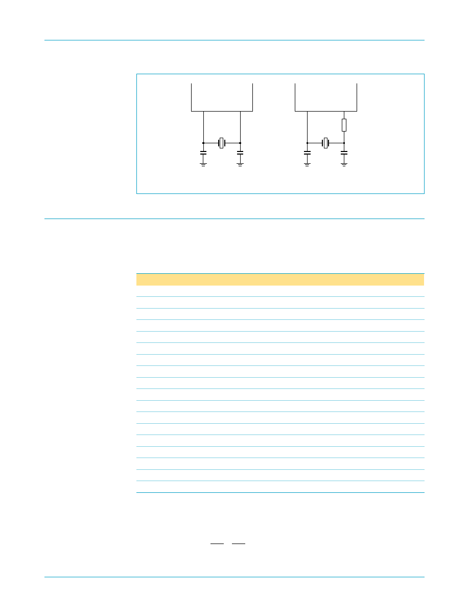
Fig 13. Crystal oscillator connections.
002aaa586
X1
1.8432 MHz
C1
22 pF
C2
47 pF
XT
AL1
XT
AL2
X1
1.8432 MHz
C1
22 pF
C2
33 pF
XT
AL1
XT
AL2
1.5 k
Table 9:
Register map - read/write properties
A2
A1
A0
Read mode
Write mode
0
0
0
receive holding register (RHR)
transmit holding register (THR)
0
0
1
interrupt enable register (IER)
interrupt enable register
0
1
0
interrupt identification register (IIR)
FIFO control register (FCR)
0
1
1
line control register (LCR)
line control register
1
0
0
modem control register (MCR)
[1]
modem control register
[1]
1
0
1
line status register (LSR)
1
1
0
modem status register (MSR)
1
1
1
scratchpad register (SPR)
scratchpad register
0
0
0
divisor latch LSB (DLL)
[2]
,
[3]
divisor latch LSB
[2]
,
[3]
0
0
1
divisor latch MSB (DLH)
[2]
,
[3]
divisor latch MSB
[2]
,
[3]
0
1
0
enhanced feature register (EFR)
[2]
,
[4]
enhanced feature register
[2]
,
[4]
1
0
0
Xon1 word
[2]
,
[4]
Xon1 word
[2]
,
[4]
1
0
1
Xon2 word
[2]
,
[4]
Xon2 word
[2]
,
[4]
1
1
0
Xoff1 word
[2]
,
[4]
Xoff1 word
[2]
,
[4]
1
1
1
Xoff2 word
[2]
,
[4]
Xoff2 word
[2]
,
[4]
1
1
0
transmission control register (TCR)
[2]
,
[5]
transmission control register
[2]
,
[5]
1
1
1
trigger level register (TLR)
[2]
,
[5]
trigger level register
[2]
,
[5]
1
1
1
FIFO ready register
[2]
,
[6]

Philips Semiconductors
SC16C752B
5 V, 3.3 V and 2.5 V dual UART, 5 Mbit/s (max.), with 64-byte FIFOs
Product data
Rev. 03 -- 14 December 2004
20 of 47
9397 750 14443
© Koninklijke Philips Electronics N.V. 2004. All rights reserved.
Table 10
lists and describes the SC16C752B internal registers.
[1]
These registers are accessible only when LCR[7] = 0.
[2]
The shaded bits in the above table can only be modified if register bit EFR[4] is enabled, i.e., if enhanced functions are enabled.
Table 10:
SC16C752B internal registers
Shaded bits are only accessible when EFR[4] is set.
A2 A1 A0 Register Bit 7
Bit 6
Bit 5
Bit 4
Bit 3
Bit 2
Bit 1
Bit 0
Read/
Write
General Register Set
[1]
0
0
0
RHR
bit 7
bit 6
bit 5
bit 4
bit 3
bit 2
bit 1
bit 0
R
0
0
0
THR
bit 7
bit 6
bit 5
bit 4
bit 3
bit 2
bit 1
bit 0
W
0
0
1
IER
0/CTS
interrupt
enable
[2]
0/RTS
interrupt
enable
[2]
0/Xoff
[2]
0/X sleep
mode
[2]
modem
status
interrupt
receive
line status
interrupt
THR
empty
interrupt
Rx data
available
interrupt
R/W
0
1
0
FCR
RX
trigger
level
(MSB)
RX trigger
level (LSB)
0/TX
trigger
level
(MSB)
[2]
0/TX
trigger
level
(LSB)
[2]
DMA
mode
select
TX FIFO
reset
RX FIFO
reset
FIFO
enable
W
0
1
0
IIR
FCR[0]
FCR[0]
0/CTS,
RTS
0/Xoff
interrupt
priority
bit 2
interrupt
priority
bit 1
interrupt
priority
bit 0
interrupt
status
R
0
1
1
LCR
DLAB
break
control bit
set parity parity
type
select
parity
enable
number of
stop bits
word
length
bit 1
word
length
bit 0
R/W
1
0
0
MCR
1
◊
or
1
◊
/4
clock
TCR and
TLR
enable
0/Xon
Any
0/enable
loop-back
IRQ
enable
OP
FIFO
ready
enable
RTS
DTR
R/W
1
0
1
LSR
0/error in
RX FIFO
THR and
TSR
empty
THR
empty
break
interrupt
framing
error
parity
error
overrun
error
data in
receiver
R
1
1
0
MSR
CD
RI
DSR
CTS
CD
RI
DSR
CTS
R
1
1
1
SPR
bit 7
bit 6
bit 5
bit 4
bit 3
bit 2
bit 1
bit 0
R/W
1
1
0
TCR
bit 7
bit 6
bit 5
bit 4
bit 3
bit 2
bit 1
bit 0
R/W
1
1
1
TLR
bit 7
bit 6
bit 5
bit 4
bit 3
bit 2
bit 1
bit 0
R/W
1
1
1
FIFO
Rdy
0
0
RX FIFO
B status
RX FIFO
A status
0
0
TX FIFO B
status
TX FIFO
A status
R
Special Register Set
[3]
0
0
0
DLL
bit 7
bit 6
bit 5
bit 4
bit 3
bit 2
bit 1
bit 0
R/W
0
0
1
DLH
bit 15
bit 14
bit 13
bit 12
bit 11
bit 10
bit 9
bit 8
R/W
Enhanced Register Set
[4]
0
1
0
EFR
Auto
CTS
Auto RTS
Special
character
detect
Enable
enhanced
functions
[2]
software
flow
control
bit 3
software
flow
control
bit 2
software
flow
control
bit 1
software
flow
control
bit 0
R/W
1
0
0
Xon1
bit 7
bit 6
bit 5
bit 4
bit 3
bit 2
bit 1
bit 0
R/W
1
0
1
Xon2
bit 7
bit 6
bit 5
bit 4
bit 3
bit 2
bit 1
bit 0
R/W
1
1
0
Xoff1
bit 7
bit 6
bit 5
bit 4
bit 3
bit 2
bit 1
bit 0
R/W
1
1
1
Xoff2
bit 7
bit 6
bit 5
bit 4
bit 3
bit 2
bit 1
bit 0
R/W

Philips Semiconductors
SC16C752B
5 V, 3.3 V and 2.5 V dual UART, 5 Mbit/s (max.), with 64-byte FIFOs
Product data
Rev. 03 -- 14 December 2004
21 of 47
9397 750 14443
© Koninklijke Philips Electronics N.V. 2004. All rights reserved.
[3]
The Special Register set is accessible only when LCR[7] is set to a logic 1.
[4]
Enhanced Feature Register; Xon-1,2 and Xoff-1,2 are accessible only when LCR is set to `BF
Hex
'.
Remark: Refer to the notes under
Table 9
for more register access information.
7.1 Receiver holding register (RHR)
The receiver section consists of the receiver holding register (RHR) and the receiver
shift register (RSR). The RHR is actually a 64-byte FIFO. The RSR receives serial
data from the RX terminal. The data is converted to parallel data and moved to the
RHR. The receiver section is controlled by the line control register. If the FIFO is
disabled, location zero of the FIFO is used to store the characters.
Remark: In this case, characters are overwritten if overflow occurs.
If overflow occurs, characters are lost. The RHR also stores the error status bits
associated with each character.
7.2 Transmit holding register (THR)
The transmitter section consists of the transmit holding register (THR) and the
transmit shift register (TSR). The THR is actually a 64-byte FIFO. The THR receives
data and shifts it into the TSR, where it is converted to serial data and moved out on
the TX terminal. If the FIFO is disabled, the FIFO is still used to store the byte.
Characters are lost if overflow occurs.

Philips Semiconductors
SC16C752B
5 V, 3.3 V and 2.5 V dual UART, 5 Mbit/s (max.), with 64-byte FIFOs
Product data
Rev. 03 -- 14 December 2004
22 of 47
9397 750 14443
© Koninklijke Philips Electronics N.V. 2004. All rights reserved.
7.3 FIFO control register (FCR)
This is a write-only register that is used for enabling the FIFOs, clearing the FIFOs,
setting transmitter and receiver trigger levels, and selecting the type of DMA
signalling.
Table 11
shows FIFO control register bit settings.
Table 11:
FIFO Control Register bits description
Bit
Symbol
Description
7:6
FCR[7]
(MSB),
FCR[6]
(LSB)
RCVR trigger. Sets the trigger level for the RX FIFO.
00 - 8 characters
01 - 16 characters
10 - 56 characters
11 - 60 characters
5:4
FCR[5]
(MSB),
FCR[4]
(LSB)
TX trigger. Sets the trigger level for the TX FIFO.
00 - 8 spaces
01 - 16 spaces
10 - 32 spaces
11 - 56 spaces
FCR[5:4] can only be modified and enabled when EFR[4] is set. This is
because the transmit trigger level is regarded as an enhanced function.
3
FCR[3]
DMA mode select.
Logic 0 = Set DMA mode `0'
Logic 1 = Set DMA mode `1'
2
FCR[2]
Reset TX FIFO.
Logic 0 = No FIFO transmit reset (normal default condition).
Logic 1 = Clears the contents of the transmit FIFO and resets the
FIFO counter logic (the transmit shift register is not cleared or
altered). This bit will return to a logic 0 after clearing the FIFO.
1
FCR[1]
Reset RX FIFO.
Logic 0 = No FIFO receive reset (normal default condition).
Logic 1 = Clears the contents of the receive FIFO and resets the FIFO
counter logic (the receive shift register is not cleared or altered). This
bit will return to a logic 0 after clearing the FIFO.
0
FCR[0]
FIFO enable.
Logic 0 = Disable the transmit and receive FIFO (normal default
condition).
Logic 1 = Enable the transmit and receive FIFO.

Philips Semiconductors
SC16C752B
5 V, 3.3 V and 2.5 V dual UART, 5 Mbit/s (max.), with 64-byte FIFOs
Product data
Rev. 03 -- 14 December 2004
23 of 47
9397 750 14443
© Koninklijke Philips Electronics N.V. 2004. All rights reserved.
7.4 Line control register (LCR)
This register controls the data communication format. The word length, number of
stop bits, and parity type are selected by writing the appropriate bits to the LCR.
Table 12
shows the line control register bit settings.
Table 12:
Line Control Register bits description
Bit
Symbol
Description
7
LCR[7]
Divisor latch enable.
Logic 0 = Divisor latch disabled (normal default condition).
Logic 1 = Divisor latch enabled.
6
LCR[6]
Break control bit. When enabled, the Break control bit causes a break
condition to be transmitted (the TX output is forced to a logic 0 state).
This condition exists until disabled by setting LCR[6] to a logic 0.
Logic 0 = no TX break condition (normal default condition).
Logic 1 = forces the transmitter output (TX) to a logic 0 to alert the
communication terminal to a line break condition.
5
LCR[5]
Set parity. LCR[5] selects the forced parity format (if LCR[3] = 1).
Logic 0 = parity is not forced (normal default condition).
LCR[5] = logic 1 and LCR[4] = logic 0: parity bit is forced to a logical 1
for the transmit and receive data.
LCR[5] = logic 1 and LCR[4] = logic 1: parity bit is forced to a logical 0
for the transmit and receive data.
4
LCR[4]
Parity type select.
Logic 0 = ODD Parity is generated (if LCR[3] = 1).
Logic 1 = EVEN Parity is generated (if LCR[3] = 1).
3
LCR[3]
Parity enable.
Logic 0 = no parity (normal default condition).
Logic 1 = a parity bit is generated during transmission and the
receiver checks for received parity.
2
LCR[2]
Number of Stop bits. Specifies the number of stop bits.
0 - 1 stop bit (word length = 5, 6, 7, 8)
1 - 1.5 stop bits (word length = 5)
1 = 2 stop bits (word length = 6, 7, 8)
1:0
LCR[1:0]
Word length bits 1, 0. These two bits specify the word length to be
transmitted or received.
00 - 5 bits
01 - 6 bits
10 - 7 bits
11 - 8 bits

Philips Semiconductors
SC16C752B
5 V, 3.3 V and 2.5 V dual UART, 5 Mbit/s (max.), with 64-byte FIFOs
Product data
Rev. 03 -- 14 December 2004
24 of 47
9397 750 14443
© Koninklijke Philips Electronics N.V. 2004. All rights reserved.
7.5 Line status register (LSR)
Table 13
shows the line status register bit settings.
When the LSR is read, LSR[4:2] reflect the error bits (BI, FE, PE) of the character at
the top of the RX FIFO (next character to be read). The LSR[4:2] registers do not
physically exist, as the data read from the RX FIFO is output directly onto the output
data bus, DI[4:2], when the LSR is read. Therefore, errors in a character are identified
by reading the LSR and then reading the RHR.
LSR[7] is set when there is an error anywhere in the RX FIFO, and is cleared only
when there are no more errors remaining in the FIFO.
Reading the LSR does not cause an increment of the RX FIFO read pointer. The
RX FIFO read pointer is incremented by reading the RHR.
Table 13:
Line Status Register bits description
Bit
Symbol
Description
7
LSR[7]
FIFO data error.
Logic 0 = No error (normal default condition).
Logic 1 = At least one parity error, framing error, or break indication is
in the receiver FIFO. This bit is cleared when no more errors are
present in the FIFO.
6
LSR[6]
THR and TSR empty. This bit is the Transmit Empty indicator.
Logic 0 = Transmitter hold and shift registers are not empty.
Logic 1 = Transmitter hold and shift registers are empty.
5
LSR[5]
THR empty. This bit is the Transmit Holding Register Empty indicator.
Logic 0 = Transmit hold register is not empty.
Logic 1 = Transmit hold register is empty. The processor can now load
up to 64 bytes of data into the THR if the TX FIFO is enabled.
4
LSR[4]
Break interrupt.
Logic 0 = No break condition (normal default condition).
Logic 1 = A break condition occurred and associated byte is 00, i.e.,
RX was LOW for one character time frame.
3
LSR[3]
Framing error.
Logic 0 = No framing error in data being read from RX FIFO (normal
default condition).
Logic 1 = Framing error occurred in data being read from RX FIFO, i.e.,
received data did not have a valid stop bit.
2
LSR[2]
Parity error.
Logic 0 = No parity error (normal default condition).
Logic 1 = Parity error in data being read from RX FIFO.
1
LSR[1]
Overrun error.
Logic 0 = No overrun error (normal default condition).
Logic 1 = Overrun error has occurred.
0
LSR[0]
Data in receiver.
Logic 0 = No data in receive FIFO (normal default condition).
Logic 1 = At least one character in the RX FIFO.

Philips Semiconductors
SC16C752B
5 V, 3.3 V and 2.5 V dual UART, 5 Mbit/s (max.), with 64-byte FIFOs
Product data
Rev. 03 -- 14 December 2004
25 of 47
9397 750 14443
© Koninklijke Philips Electronics N.V. 2004. All rights reserved.
Remark: The three error bits (parity, framing, break) may not be updated correctly in
the first read of the LSR when the input clock (XTAL1) is running faster than 36 MHz.
However, the second read is always correct. It is strongly recommended that when
using this device with a clock faster than 36 MHz, that the LSR be read twice and only
the second read be used for decision making. All other bits in the LSR are correct on
all reads.
7.6 Modem control register (MCR)
The MCR controls the interface with the mode, data set, or peripheral device that is
emulating the modem.
Table 14
shows modem control register bit settings.
[1]
MCR[7:5] can only be modified when EFR[4] is set, i.e., EFR[4] is a write enable.
Table 14:
Modem Control Register bits description
Bit
Symbol
Description
7
MCR[7]
[1]
Clock select.
Logic 0 = Divide-by-1 clock input.
Logic 1 = Divide-by-4 clock input.
6
MCR[6]
[1]
TCR and TLR enable.
Logic 0 = no action.
Logic 1 = Enable access to the TCR and TLR registers.
5
MCR[5]
[1]
Xon Any.
Logic 0 = Disable Xon Any function.
Logic 1 = Enable Xon Any function.
4
MCR[4]
Enable loop-back.
Logic 0 = Normal operating mode.
Logic 1 = Enable local loop-back mode (internal). In this mode the
MCR[3:0] signals are looped back into MSR[7:4] and the TX output
is looped back to the RX input internally.
3
MCR[3]
IRQ enable OP.
Logic 0 = Forces INTA-INTB outputs to the 3-State mode and OP
output to HIGH state.
Logic 1 = Forces the INTA-INTB outputs to the active state and OP
output to LOW state. In loop-back mode, controls MSR[7].
2
MCR[2]
FIFO Ready enable.
Logic 0 = Disable the FIFO Rdy register.
Logic 1 = Enable the FIFO Rdy register.
In loop-back mode, controls MSR[6].
1
MCR[1]
RTS
Logic 0 = Force RTS output to inactive (HIGH).
Logic 1 = Force RTS output to active (LOW).
In loop-back mode, controls MSR[4]. If Auto-RTS is enabled, the
RTS output is controlled by hardware flow control.
0
MCR[0]
DTR
Logic 0 = Force DTR output to inactive (HIGH).
Logic 1 = Force DTR output to active (LOW).
In loop-back mode, controls MSR[5].

Philips Semiconductors
SC16C752B
5 V, 3.3 V and 2.5 V dual UART, 5 Mbit/s (max.), with 64-byte FIFOs
Product data
Rev. 03 -- 14 December 2004
26 of 47
9397 750 14443
© Koninklijke Philips Electronics N.V. 2004. All rights reserved.
7.7 Modem status register (MSR)
This 8-bit register provides information about the current state of the control lines
from the mode, data set, or peripheral device to the processor. It also indicates when
a control input from the modem changes state.
Table 15
shows modem status
register bit settings per channel.
[1]
The primary inputs RI, CD, CTS, DSR are all Active-LOW, but their registered equivalents in the MSR
and MCR (in loop-back) registers are Active-HIGH.
7.8 Interrupt enable register (IER)
The interrupt enable register (IER) enables each of the six types of interrupt, receiver
error, RHR interrupt, THR interrupt, Xoff received, or CTS/RTS change of state from
LOW to HIGH. The INT output signal is activated in response to interrupt generation.
Table 16
shows interrupt enable register bit settings.
Table 15:
Modem Status Register bits description
Bit
Symbol
Description
7
MSR[7]
CD (Active-HIGH, logical 1). This bit is the complement of the CD input
during normal mode. During internal loop-back mode, it is equivalent to
MCR[3].
6
MSR[6]
RI (Active-HIGH, logical 1). This bit is the complement of the RI input
during normal mode. During internal loop-back mode, it is equivalent to
MCR[2].
5
MSR[5]
DSR (Active-HIGH, logical 1). This bit is the complement of the DSR
input during normal mode. During internal loop-back mode, it is
equivalent MCR[0].
4
MSR[4]
CTS (Active-HIGH, logical 1). This bit is the complement of the CTS
input during normal mode. During internal loop-back mode, it is
equivalent to MCR[1].
3
MSR[3]
CD. Indicates that CD input (or MCR[3] in loop-back mode) has
changed state. Cleared on a read.
2
MSR[2]
RI. Indicates that RI input (or MCR[2] in loop-back mode) has changed
state from LOW to HIGH. Cleared on a read.
1
MSR[1]
DSR. Indicates that DSR input (or MCR[0] in loop-back mode) has
changed state. Cleared on a read.
0
MSR[0]
CTS. Indicates that CTS input (or MCR[1] in loop-back mode) has
changed state. Cleared on a read.
Table 16:
Interrupt Enable Register bits description
Bit
Symbol
Description
7
IER[7]
[1]
CTS interrupt enable.
Logic 0 = Disable the CTS interrupt (normal default condition).
Logic 1 = Enable the CTS interrupt.
6
IER[6]
[1]
RTS interrupt enable.
Logic 0 = Disable the RTS interrupt (normal default condition).
Logic 1 = Enable the RTS interrupt.
5
IER[5]
[1]
Xoff interrupt.
Logic 0 = Disable the Xoff interrupt (normal default condition).
Logic 1 = Enable the Xoff interrupt.

Philips Semiconductors
SC16C752B
5 V, 3.3 V and 2.5 V dual UART, 5 Mbit/s (max.), with 64-byte FIFOs
Product data
Rev. 03 -- 14 December 2004
27 of 47
9397 750 14443
© Koninklijke Philips Electronics N.V. 2004. All rights reserved.
[1]
IER[7:4] can only be modified if EFR[4] is set, i.e., EFR[4] is a write enable. Re-enabling IER[1] will
not cause a new interrupt if the THR is below the threshold.
7.9 Interrupt identification register (IIR)
The IIR is a read-only 8-bit register which provides the source of the interrupt in a
prioritized manner.
Table 17
shows interrupt identification register bit settings.
The interrupt priority list is shown in
Table 18
.
4
IER[4]
[1]
Sleep mode.
Logic 0 = Disable sleep mode (normal default condition).
Logic 1 = Enable sleep mode. See
Section 6.7 "Sleep mode"
for details.
3
IER[3]
Modem Status Interrupt.
Logic 0 = Disable the modem status register interrupt (normal default
condition).
Logic 1 = Enable the modem status register interrupt.
2
IER[2]
Receive Line Status interrupt.
Logic 0 = Disable the receiver line status interrupt (normal default
condition).
Logic 1 = Enable the receiver line status interrupt.
1
IER[1]
Transmit Holding Register interrupt.
Logic 0 = Disable the THR interrupt (normal default condition).
Logic 1 = Enable the THR interrupt.
0
IER[0]
Receive Holding Register interrupt.
Logic 0 = Disable the RHR interrupt (normal default condition).
Logic 1 = Enable the RHR interrupt.
Table 16:
Interrupt Enable Register bits description
...continued
Bit
Symbol
Description
Table 17:
Interrupt Identification Register bits description
Bit
Symbol
Description
7:6
IIR[7:6]
Mirror the contents of FCR[0].
5
IIR[5]
RTS/CTS LOW-to-HIGH change of state.
4
IIR[4]
1 = Xoff/Special character has been detected.
3:1
IIR[3:1]
3-bit encoded interrupt. See
Table 18
.
0
IIR[0]
Interrupt status.
Logic 0 = An interrupt is pending.
Logic 1 = No interrupt is pending.

Philips Semiconductors
SC16C752B
5 V, 3.3 V and 2.5 V dual UART, 5 Mbit/s (max.), with 64-byte FIFOs
Product data
Rev. 03 -- 14 December 2004
28 of 47
9397 750 14443
© Koninklijke Philips Electronics N.V. 2004. All rights reserved.
7.10 Enhanced feature register (EFR)
This 8-bit register enables or disables the enhanced features of the UART.
Table 19
shows the enhanced feature register bit settings.
Table 18:
Interrupt priority list
Priority
level
IIR[5]
IIR[4]
IIR[3]
IIR[2]
IIR[1]
IIR[0]
Source of the interrupt
1
0
0
0
1
1
0
Receiver Line Status error
2
0
0
1
1
0
0
Receiver time-out interrupt
2
0
0
0
1
0
0
RHR interrupt
3
0
0
0
0
1
0
THR interrupt
4
0
0
0
0
0
0
Modem interrupt
5
0
1
0
0
0
0
Received Xoff signal/
special character
6
1
0
0
0
0
0
CTS, RTS change of state
from active (LOW) to
inactive (HIGH)
Table 19:
Enhanced Feature Register bits description
Bit
Symbol
Description
7
EFR[7]
CTS flow control enable.
Logic 0 = CTS flow control is disabled (normal default condition).
Logic 1 = CTS flow control is enabled. Transmission will stop when a
HIGH signal is detected on the CTS pin.
6
EFR[6]
RTS flow control enable.
Logic 0 = RTS flow control is disabled (normal default condition).
Logic 1 = RTS flow control is enabled. The RTS pin goes HIGH when
the receiver FIFO HALT trigger level TCR[3:0] is reached, and goes
LOW when the receiver FIFO RESUME transmission trigger level
TCR[7:4] is reached.
5
EFR[5]
Special character detect.
Logic 0 = Special character detect disabled (normal default condition).
Logic 1 = Special character detect enabled. Received data is
compared with Xoff-2 data. If a match occurs, the received data is
transferred to FIFO and IIR[4] is set to a logical 1 to indicate a special
character has been detected.
4
EFR[4]
Enhanced functions enable bit.
Logic 0 = Disables enhanced functions and writing to IER[7:4],
FCR[5:4], MCR[7:5].
Logic 1 = Enables the enhanced function IER[7:4], FCR[5:4], and
MCR[7:5] can be modified, i.e., this bit is therefore a write enable.
3:0
EFR[3:0]
Combinations of software flow control can be selected by programming
these bits. See
Table 3 "Software flow control options (EFR[0:3])" on
page 9
.

Philips Semiconductors
SC16C752B
5 V, 3.3 V and 2.5 V dual UART, 5 Mbit/s (max.), with 64-byte FIFOs
Product data
Rev. 03 -- 14 December 2004
29 of 47
9397 750 14443
© Koninklijke Philips Electronics N.V. 2004. All rights reserved.
7.11 Divisor latches (DLL, DLH)
These are two 8-bit registers which store the 16-bit divisor for generation of the baud
clock in the baud rate generator. DLH stores the most significant part of the divisor.
DLL stores the least significant part of the divisor.
Note that DLL and DLH can only be written to before sleep mode is enabled, i.e.,
before IER[4] is set.
7.12 Transmission control register (TCR)
This 8-bit register is used to store the RX FIFO threshold levels to stop/start
transmission during hardware/software flow control.
Table 20
shows transmission
control register bit settings.
TCR trigger levels are available from 0-60 bytes with a granularity of four.
Remark: TCR can only be written to when EFR[4] = 1 and MCR[6] = 1. The
programmer must program the TCR such that TCR[3:0] > TCR[7:4]. There is no
built-in hardware check to make sure this condition is met. Also, the TCR must be
programmed with this condition before Auto-RTS or software flow control is enabled
to avoid spurious operation of the device.
7.13 Trigger level register (TLR)
This 8-bit register is pulsed to store the transmit and received FIFO trigger levels
used for DMA and interrupt generation. Trigger levels from 4-60 can be programmed
with a granularity of 4.
Table 21
shows trigger level register bit settings.
Remark: TLR can only be written to when EFR[4] = 1 and MCR[6] = 1. If TLR[3:0] or
TLR[7:4] are logical 0, the selectable trigger levels via the FIFO control register (FCR)
are used for the transmit and receive FIFO trigger levels. Trigger levels from 4-60
bytes are available with a granularity of four. The TLR should be programmed for
N
/
4
,
where N is the desired trigger level.
When the trigger level setting in TLR is zero, the SC16C752B uses the trigger level
setting defined in FCR. If TLR has non-zero trigger level value, the trigger level
defined in FCR is discarded. This applies to both transmit FIFO and receive FIFO
trigger level setting.
When TLR is used for RX trigger level control, FCR[7:6] should be left at the default
state, i.e., `00'.
Table 20:
Transmission Control Register bits description
Bit
Symbol
Description
7:4
TCR[7:4]
RX FIFO trigger level to resume transmission (0-60).
3:0
TCR[3:0]
RX FIFO trigger level to halt transmission (0-60).
Table 21:
Trigger Level Register bits description
Bit
Symbol
Description
7:4
TLR[7:4]
RX FIFO trigger levels (4-60), number of characters available.
3:0
TLR[3:0]
TX FIFO trigger levels (4-60), number of spaces available.

Philips Semiconductors
SC16C752B
5 V, 3.3 V and 2.5 V dual UART, 5 Mbit/s (max.), with 64-byte FIFOs
Product data
Rev. 03 -- 14 December 2004
30 of 47
9397 750 14443
© Koninklijke Philips Electronics N.V. 2004. All rights reserved.
7.14 FIFO ready register
The FIFO ready register provides real-time status of the transmit and receive FIFOs
of both channels.
The FIFO Rdy register is a read-only register that can be accessed when any of the
two UARTs is selected CSA or CSB = 0, MCR[2] (FIFO Rdy Enable) is a logic 1, and
loop-back is disabled. The address is 111.
Table 22:
FIFO Ready Register bits description
Bit
Symbol
Description
7:6
FIFO Rdy[7:6]
Unused; always 0.
5
FIFO Rdy[5]
RX FIFO B status. Related to DMA.
4
FIFO Rdy[4]
RX FIFO A status. Related to DMA.
3:2
FIFO Rdy[3:2]
Unused; always 0.
1
FIFO Rdy[1]
TX FIFO B status. Related to DMA.
0
FIFO Rdy[0]
TX FIFO A status. Related to DMA.

Philips Semiconductors
SC16C752B
5 V, 3.3 V and 2.5 V dual UART, 5 Mbit/s (max.), with 64-byte FIFOs
Product data
Rev. 03 -- 14 December 2004
31 of 47
9397 750 14443
© Koninklijke Philips Electronics N.V. 2004. All rights reserved.
8.
Programmer's guide
The base set of registers that is used during high-speed data transfer have a
straightforward access method. The extended function registers require special
access bits to be decoded along with the address lines. The following guide will help
with programming these registers. Note that the descriptions below are for individual
register access. Some streamlining through interleaving can be obtained when
programming all the registers.
Table 23:
Register programming guide
Command
Actions
Set baud rate to VALUE1, VALUE2
Read LCR (03), save in temp
Set LCR (03) to 80
Set DLL (00) to VALUE1
SET DLM (01) to VALUE2
Set LCR (03) to temp
Set Xoff-1, Xon-1 to VALUE1, VALUE2
Read LCR (03), save in temp
Set LCR (03) to BF
Set Xoff-1 (06) to VALUE1
SET Xon-1 (04) to VALUE2
Set LCR (03) to temp
Set Xoff-2, Xon-2 to VALUE1, VALUE2
Read LCR (03), save in temp
Set LCR (03) to BF
Set Xoff-2 (07) to VALUE1
SET Xon-2 (05) to VALUE2
Set LCR (03) to temp
Set software flow control mode to
VALUE
Read LCR (03), save in temp
Set LCR (03) to BF
Set EFR (02) to VALUE
Set LCR (03) to temp
Set flow control threshold to VALUE
Read LCR (03), save in temp1
Set LCR (03) to BF
Read EFR (02), save in temp2
Set EFR (02) to 10 + temp2
Set LCR (03) to 00
Read MCR (04), save in temp3
Set MCR (04) to 40 + temp3
Set TCR (06) to VALUE
Set MCR (04) to temp3
Set LCR (03) to BF
Set EFR (02) to temp2
Set LCR (03) to temp1

Philips Semiconductors
SC16C752B
5 V, 3.3 V and 2.5 V dual UART, 5 Mbit/s (max.), with 64-byte FIFOs
Product data
Rev. 03 -- 14 December 2004
32 of 47
9397 750 14443
© Koninklijke Philips Electronics N.V. 2004. All rights reserved.
[1]
◊
sign here means bit-AND.
Set TX FIFO and RX FIFO thresholds
to VALUE
Read LCR (03), save in temp1
Set LCR (03) to BF
Read EFR (02), save in temp2
Set EFR (02) to 10 + temp2
Set LCR (03) to 00
Read MCR (04), save in temp3
Set MCR (04) to 40 + temp3
Set TLR (07) to VALUE
Set MCR (04) to temp3
Set LCR (03) to BF
Set EFR (02) to temp2
Set LCR (03) to temp1
Read FIFO Rdy register
Read MCR (04), save in temp1
Set temp2 = temp1
◊
EF
[1]
Set MCR (04) = 40 + temp2
Read FFR (07), save in temp2
Pass temp2 back to host
Set MCR (04) to temp1
Set prescaler value to divide-by-1
Read LCR (03), save in temp1
Set LCR (03) to BF
Read EFR (02), save in temp2
Set EFR (02) to 10 + temp2
Set LCR (03) to 00
Read MCR (04), save in temp3
Set MCR (04) to temp3
◊
7F
[1]
Set LCR (03) to BF
Set EFR (02) to temp2
Set LCR (03) to temp1
Set prescaler value to divide-by-4
Read LCR (03), save in temp1
Set LCR (03) to BF
Read EFR (02), save in temp2
Set EFR (02) to 10 + temp2
Set LCR (03) to 00
Read MCR (04), save in temp3
Set MCR (04) to temp3 + 80
Set LCR (03) to BF
Set EFR (02) to temp2
Set LCR (03) to temp1
Table 23:
Register programming guide
...continued
Command
Actions

Philips Semiconductors
SC16C752B
5 V, 3.3 V and 2.5 V dual UART, 5 Mbit/s (max.), with 64-byte FIFOs
Product data
Rev. 03 -- 14 December 2004
33 of 47
9397 750 14443
© Koninklijke Philips Electronics N.V. 2004. All rights reserved.
9.
Limiting values
[1]
Stresses beyond those listed under Limiting values may cause permanent damage to the device. These are stress ratings only, and
functional operation of the device at these or any other conditions beyond those indicated under "recommended operating conditions" is
not implied. Exposure to absolute-maximum-rated conditions for extended periods may affect device reliability.
10. Static characteristics
[1]
Meets TTL levels, V
IO(min)
= 2 V and V
IH(max)
= 0.8 V on non-hysteresis inputs.
[2]
Applies for external output buffers.
Table 24:
Limiting values
In accordance with the Absolute Maximum Rating System (IEC 60134).
Symbol
Parameter
Conditions
Min
Max
Unit
V
CC
supply voltage
-
7
V
V
I
input voltage
-
0.3
V
CC
+ 0.3
V
V
O
output voltage
-
0.3
V
CC
+ 0.3
V
T
amb
operating ambient temperature
in free-air
-
40
+85
∞
C
T
stg
storage temperature
-
65
+150
∞
C
Table 25:
DC electrical characteristics
V
CC
= 2.5 V, 3.3 V
±
10% or 5 V
±
10%.
Symbol
Parameter
Conditions
2.5 V
3.3 V and 5 V
Unit
Min
Nom
Max
Min
Nom
Max
V
CC
supply voltage
V
CC
-
10% V
CC
V
CC
+ 10% V
CC
-
10% V
CC
V
CC
+ 10% V
V
I
input voltage
0
-
V
CC
0
-
V
CC
V
V
IH
HIGH-level input
voltage
[1]
1.6
-
V
CC
2.0
-
V
CC
V
V
IL
LOW-level input
voltage
[1]
-
-
0.65
-
-
0.8
V
V
O
output voltage
[2]
0
-
V
CC
0
-
V
CC
V
V
OH
HIGH-level output
voltage
I
OH
=
-
8 mA
[4]
-
-
-
2.0
-
-
V
I
OH
=
-
4 mA
[5]
-
-
-
2.0
-
-
V
I
OH
=
-
800
µ
A
[4]
1.85
-
-
-
-
-
V
I
OH
=
-
400
µ
A
[5]
1.85
-
-
-
-
-
V
V
OL
LOW-level output
voltage
[7]
I
OL
= 8 mA
[4]
-
-
-
-
-
0.4
V
I
OL
= 4 mA
[5]
-
-
-
-
-
0.4
V
I
OL
= 2 mA
[4]
-
-
0.4
-
-
-
V
I
OL
= 1.6 mA
[5]
-
-
0.4
-
-
-
V
C
i
input capacitance
-
-
18
-
-
18
pF
T
amb
operating ambient
temperature
-
40
25
85
-
40
25
85
∞
C
T
j
junction
temperature
[3]
0
25
125
0
25
125
∞
C
clock speed
[8]
-
-
50
-
-
80
MHz
clock duty cycle
-
50
-
-
50
-
%
I
CC
supply current
f = 5 MHz
[6]
-
-
3.5
-
-
4.5
mA

Philips Semiconductors
SC16C752B
5 V, 3.3 V and 2.5 V dual UART, 5 Mbit/s (max.), with 64-byte FIFOs
Product data
Rev. 03 -- 14 December 2004
34 of 47
9397 750 14443
© Koninklijke Philips Electronics N.V. 2004. All rights reserved.
[3]
These junction temperatures reflect simulated conditions. Absolute maximum junction temperature is 150
∞
C. The customer is
responsible for verifying junction temperature.
[4]
These parameters apply for D7-D0.
[5]
These parameters apply for DTRA, DTRB, INIA, INTB, RTSA, RTSB, RXRDYA, RXRDYB, TXRDYA, TXRDYB, TXA, TXB.
[6]
Measurement condition, normal operation other than sleep mode:
V
CC
= 3.3 V; T
amb
= 25
∞
C. Full duplex serial activity on all two serial (UART) channels at the clock frequency specified in the
recommended operating conditions with divisor of 1.
[7]
Except x
2
, V
OL
= 1 V typical.
[8]
Applies to external clock; crystal oscillator max. 24 MHz.
11. Dynamic characteristics
Table 26:
AC electrical characteristics
T
amb
=
-
40
∞
C to +85
∞
C; V
CC
= 2.5 V, 3.3 V
±
10% or 5 V
±
10%, unless specified otherwise.
Symbol
Parameter
Conditions
2.5 V
3.3 V and 5 V
Unit
Min
Max
Min
Max
t
d1
IOR delay from chip select
10
-
0
-
ns
t
d2
read cycle delay
25 pF load
20
-
20
-
ns
t
d3
delay from IOR to data
25 pF load
-
77
-
26
ns
t
d4
data disable time
25 pF load
-
15
-
15
ns
t
d5
IOW delay from chip select
10
-
10
-
ns
t
d6
write cycle delay
25
-
25
-
ns
t
d7
delay from IOW to output
25 pF load
-
100
-
33
ns
t
d8
delay to set interrupt from modem input
25 pF load
-
100
-
24
ns
t
d9
delay to reset interrupt from IOR
25 pF load
-
100
-
24
ns
t
d10
delay from stop to set interrupt
-
1
-
1
R
clk
baud
rate
t
d11
delay from IOR to reset interrupt
25 pF load
-
100
-
29
ns
t
d12
delay from start to set interrupt
-
100
-
100
ns
t
d13
delay from IOW to transmit start
8
24
8
24
R
clk
baud
rate
t
d14
delay from IOW to reset interrupt
-
100
-
70
ns
t
d15
delay from stop to set RXRDY
-
1
-
1
R
clk
baud
rate
t
d16
delay from IOR to reset RXRDY
-
100
-
75
ns
t
d17
delay from IOW to set TXRDY
-
100
-
70
ns
t
d18
delay from start to reset TXRDY
-
16
-
16
R
clk
baud
rate
t
d19
delay between successive assertion of
IOW and IOR
-
20
-
20
ns
t
h1
chip select hold time from IOR
0
-
0
-
ns
t
h2
chip select hold time from IOW
0
-
0
-
ns
t
h3
data hold time
15
-
15
-
ns
t
h4
address hold time
0
-
0
-
ns
t
h5
hold time from XTAL1 clock
HIGH-to-LOW transition to IOW or IOR
release
20
-
20
-
ns

Philips Semiconductors
SC16C752B
5 V, 3.3 V and 2.5 V dual UART, 5 Mbit/s (max.), with 64-byte FIFOs
Product data
Rev. 03 -- 14 December 2004
35 of 47
9397 750 14443
© Koninklijke Philips Electronics N.V. 2004. All rights reserved.
[1]
Applies to external clock; crystal oscillator max 24 MHz.
11.1 Timing diagrams
t
p1
, t
p2
clock cycle period
10
-
6
-
ns
t
p3
clock speed
[1]
-
48
-
80
MHz
t
(RESET)
RESET pulse width
200
-
200
-
ns
t
su1
address set-up time
0
-
0
-
ns
t
su2
data set-up time
16
-
16
-
ns
t
su3
set-up time from IOW or IOR assertion
to XTAL1 clock LOW-to-HIGH transition
20
-
20
-
ns
t
w1
IOR strobe width
77
-
30
-
ns
t
w2
IOW strobe width
30
-
30
-
ns
Table 26:
AC electrical characteristics
...continued
T
amb
=
-
40
∞
C to +85
∞
C; V
CC
= 2.5 V, 3.3 V
±
10% or 5 V
±
10%, unless specified otherwise.
Symbol
Parameter
Conditions
2.5 V
3.3 V and 5 V
Unit
Min
Max
Min
Max
Fig 14. General read timing.
DATA
ACTIVE
ACTIVE
VALID
ADDRESS
002aaa235
tsu1
th4
td1
tw1
td2
td3
td4
A0≠A2
CSA,
CSB
IOR
D0≠D7
th1
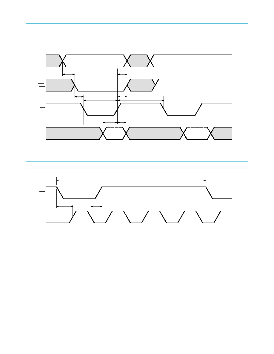
Philips Semiconductors
SC16C752B
5 V, 3.3 V and 2.5 V dual UART, 5 Mbit/s (max.), with 64-byte FIFOs
Product data
Rev. 03 -- 14 December 2004
36 of 47
9397 750 14443
© Koninklijke Philips Electronics N.V. 2004. All rights reserved.
Fig 15. General write timing.
DATA
ACTIVE
ACTIVE
VALID
ADDRESS
002aaa236
tsu1
th4
td5
tw2
td6
tsu2
th3
A0≠A2
CSA,
CSB
IOW
D0≠D7
th2
Fig 16. Alternate read/write strobe timing.
002aaa237
th5
IOW
IOR
XTAL1
td19
tsu3
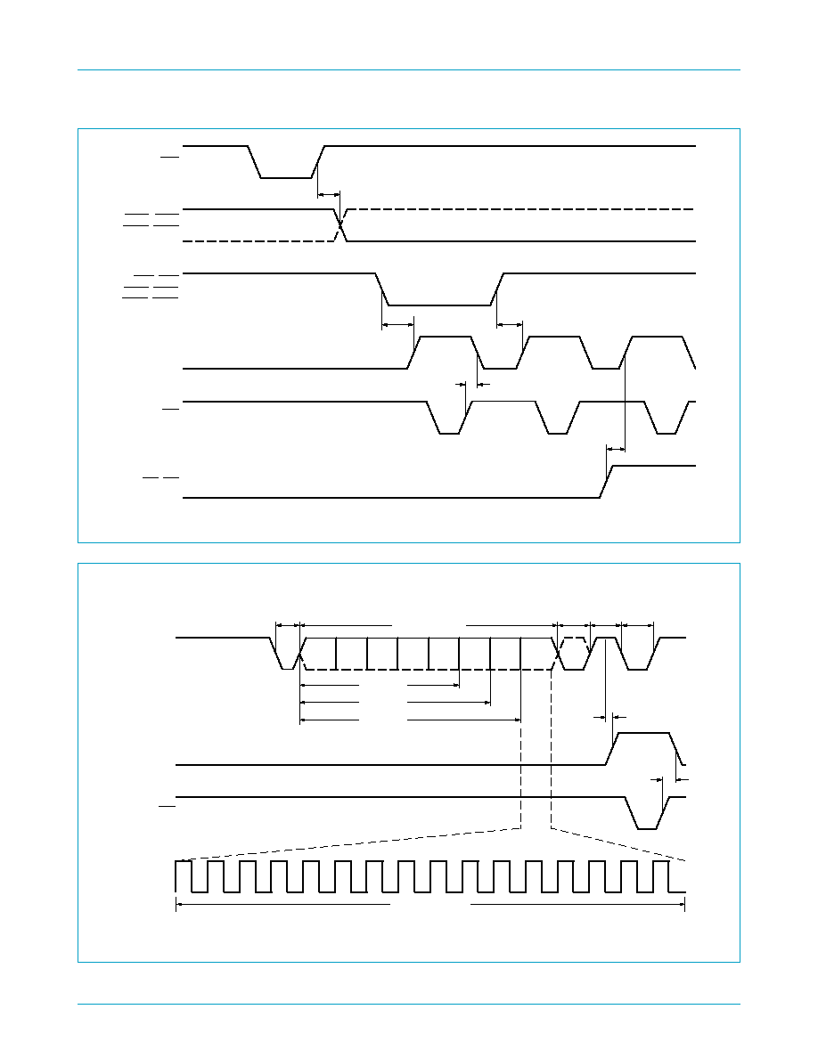
Philips Semiconductors
SC16C752B
5 V, 3.3 V and 2.5 V dual UART, 5 Mbit/s (max.), with 64-byte FIFOs
Product data
Rev. 03 -- 14 December 2004
37 of 47
9397 750 14443
© Koninklijke Philips Electronics N.V. 2004. All rights reserved.
Fig 17. Modem input/output timing.
t
d7
change of state
t
d8
t
d8
t
d9
002aaa238
t
d8
change of state
change of state
change of state
active
active
active
active
active
active
active
change of state
RTSA, RTSB
DTRA, DTRB
IOW
CDA, CDB
CTSA, CTSB
DSRA, DSRB
INTA, INTB
IOR
RIA, RIB
Fig 18. Receive timing.
D0
D1
D2
D3
D4
D5
D6
D7
active
active
16 baud rate clock
002aaa239
t
d11
next
data
Start
bit
Stop
bit
parity
bit
Start
bit
t
d10
RXA, RXB
INTA, INTB
IOR
data bits (0 to 7)
5 data bits
6 data bits
7 data bits
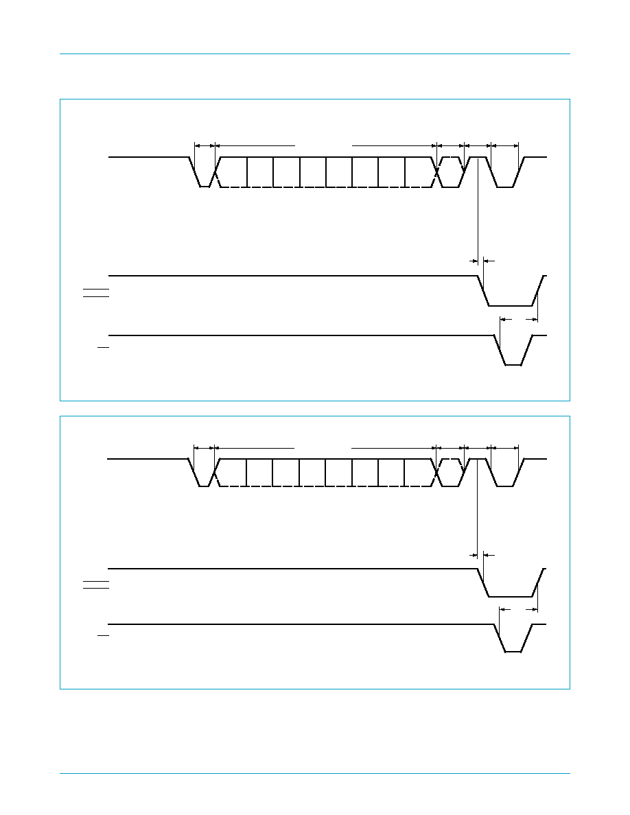
Philips Semiconductors
SC16C752B
5 V, 3.3 V and 2.5 V dual UART, 5 Mbit/s (max.), with 64-byte FIFOs
Product data
Rev. 03 -- 14 December 2004
38 of 47
9397 750 14443
© Koninklijke Philips Electronics N.V. 2004. All rights reserved.
Fig 19. Receive ready timing in non-FIFO mode.
D0
D1
D2
D3
D4
D5
D6
D7
ACTIVE
DATA
READY
ACTIVE
002aaa240
td16
NEXT
DATA
START
BIT
STOP
BIT
PARITY
BIT
START
BIT
td15
RXA
RXB
RXRDYA
RXRDYB
IOR
DATA BITS (5-8)
Fig 20. Receive ready timing in FIFO mode.
D0
D1
D2
D3
D4
D5
D6
D7
ACTIVE
DATA
READY
ACTIVE
002aaa241
td16
STOP
BIT
PARITY
BIT
START
BIT
td15
RXA
RXB
RXRDYA
RXRDYB
IOR
DATA BITS (5-8)
FIRST BYTE THAT
REACHES THE
TRIGGER LEVEL
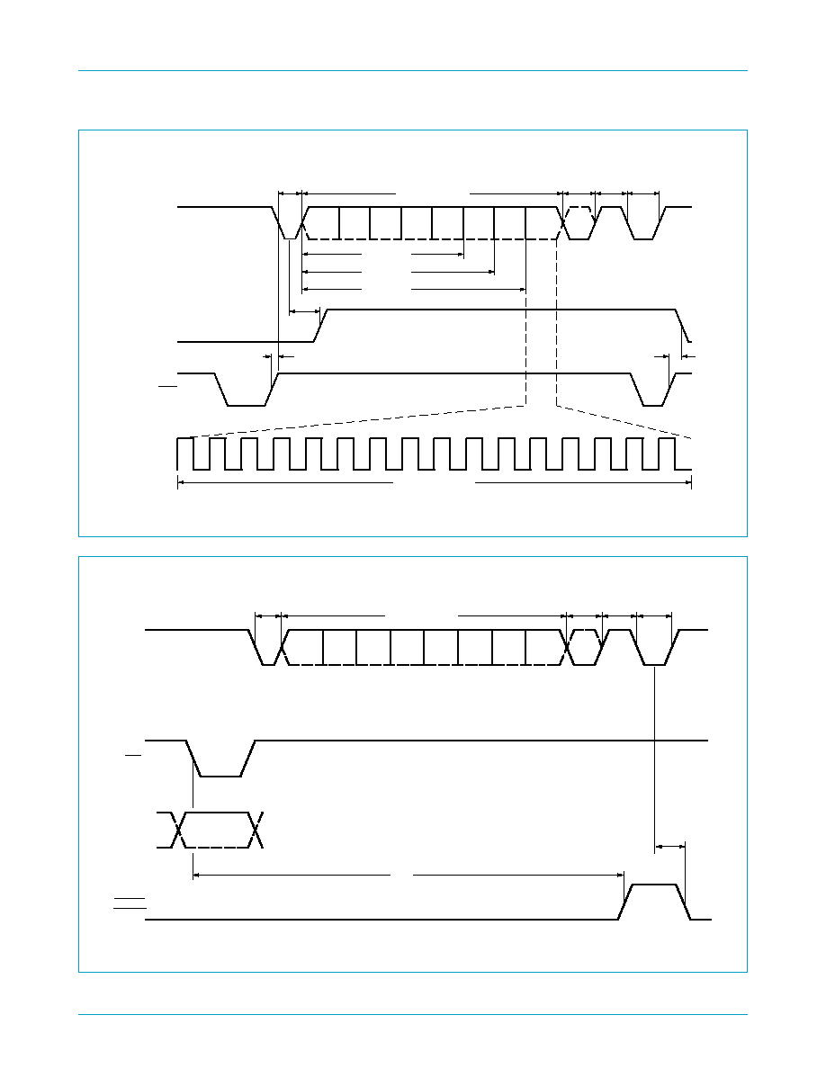
Philips Semiconductors
SC16C752B
5 V, 3.3 V and 2.5 V dual UART, 5 Mbit/s (max.), with 64-byte FIFOs
Product data
Rev. 03 -- 14 December 2004
39 of 47
9397 750 14443
© Koninklijke Philips Electronics N.V. 2004. All rights reserved.
Fig 21. Transmit timing.
D0
D1
D2
D3
D4
D5
D6
D7
active
TX ready
active
16 baud rate clock
002aaa242
t
d14
Start
bit
t
d12
TXA, TXB
INTA, INTB
IOW
data bits (0 to 7)
active
t
d13
5 data bits
6 data bits
7 data bits
parity
bit
Stop
bit
next
data
Start
bit
Fig 22. Transmit ready timing in non-FIFO mode.
D0
D1
D2
D3
D4
D5
D6
D7
TRANSMITTER
NOT READY
002aaa243
NEXT
DATA
START
BIT
STOP
BIT
PARITY
BIT
START
BIT
td17
TXA,
TXB
TXRDYA,
TXRDYB
IOW
DATA BITS (5-8)
ACTIVE
D0≠D7
BYTE #1
ACTIVE
TRANSMITTER READY
td18
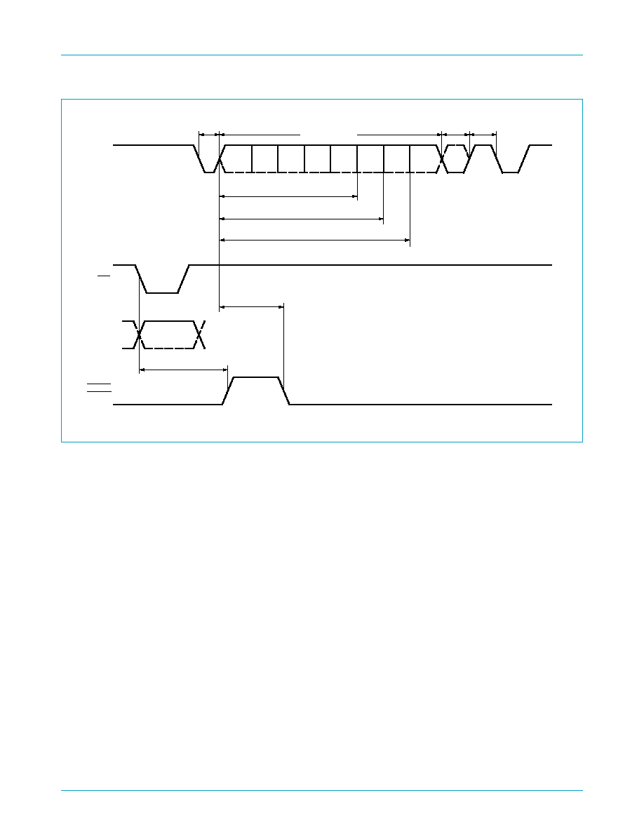
Philips Semiconductors
SC16C752B
5 V, 3.3 V and 2.5 V dual UART, 5 Mbit/s (max.), with 64-byte FIFOs
Product data
Rev. 03 -- 14 December 2004
40 of 47
9397 750 14443
© Koninklijke Philips Electronics N.V. 2004. All rights reserved.
Fig 23. Transmit ready timing in FIFO mode.
D0
D1
D2
D3
D4
D5
D6
D7
TRIGGER
LEAD
002aaa244
STOP
BIT
PARITY
BIT
START
BIT
td17
TXA,
TXB
TXRDYA,
TXRDYB
IOW
DATA BITS (5-8)
ACTIVE
D0≠D7
BYTE #32
5 DATA BITS
6 DATA BITS
7 DATA BITS
td18
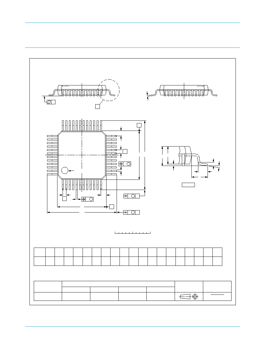
Philips Semiconductors
SC16C752B
5 V, 3.3 V and 2.5 V dual UART, 5 Mbit/s (max.), with 64-byte FIFOs
Product data
Rev. 03 -- 14 December 2004
41 of 47
9397 750 14443
© Koninklijke Philips Electronics N.V. 2004. All rights reserved.
12. Package outline
Fig 24. LQFP48 (SOT313-2).
UNIT
A
max.
A
1
A
2
A
3
b
p
c
E
(1)
e
H
E
L
L
p
Z
y
w
v
REFERENCES
OUTLINE
VERSION
EUROPEAN
PROJECTION
ISSUE DATE
IEC
JEDEC
JEITA
mm
1.6
0.20
0.05
1.45
1.35
0.25
0.27
0.17
0.18
0.12
7.1
6.9
0.5
9.15
8.85
0.95
0.55
7
0
o
o
0.12
0.1
0.2
1
DIMENSIONS (mm are the original dimensions)
Note
1. Plastic or metal protrusions of 0.25 mm maximum per side are not included.
0.75
0.45
SOT313-2
MS-026
136E05
00-01-19
03-02-25
D
(1)
(1)
(1)
7.1
6.9
H
D
9.15
8.85
E
Z
0.95
0.55
D
b
p
e
E
B
12
D
H
b
p
E
H
v
M
B
D
ZD
A
Z E
e
v
M
A
1
48
37
36
25
24
13
A
1
A
L
p
detail X
L
(A )
3
A
2
X
y
c
w
M
w
M
0
2.5
5 mm
scale
pin 1 index
LQFP48: plastic low profile quad flat package; 48 leads; body 7 x 7 x 1.4 mm
SOT313-2
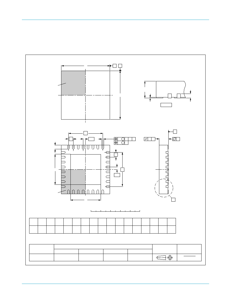
Philips Semiconductors
SC16C752B
5 V, 3.3 V and 2.5 V dual UART, 5 Mbit/s (max.), with 64-byte FIFOs
Product data
Rev. 03 -- 14 December 2004
42 of 47
9397 750 14443
© Koninklijke Philips Electronics N.V. 2004. All rights reserved.
Fig 25. HVQFN32 (SOT617-1).
0.5
1
A1
Eh
b
UNIT
y
e
0.2
c
REFERENCES
OUTLINE
VERSION
EUROPEAN
PROJECTION
ISSUE DATE
IEC
JEDEC
JEITA
mm
5.1
4.9
Dh
3.25
2.95
y1
5.1
4.9
3.25
2.95
e1
3.5
e2
3.5
0.30
0.18
0.05
0.00
0.05
0.1
DIMENSIONS (mm are the original dimensions)
SOT617-1
MO-220
- - -
- - -
0.5
0.3
L
0.1
v
0.05
w
0
2.5
5 mm
scale
SOT617-1
HVQFN32: plastic thermal enhanced very thin quad flat package; no leads;
32 terminals; body 5 x 5 x 0.85 mm
A
(1)
max.
A
A1
c
detail X
y
y1 C
e
L
Eh
Dh
e
e1
b
9
16
32
25
24
17
8
1
X
D
E
C
B
A
e2
terminal 1
index area
terminal 1
index area
01-08-08
02-10-18
1/2
e
1/2
e
A
C
C
B
v
M
w
M
E
(1)
Note
1. Plastic or metal protrusions of 0.075 mm maximum per side are not included.
D
(1)

Philips Semiconductors
SC16C752B
5 V, 3.3 V and 2.5 V dual UART, 5 Mbit/s (max.), with 64-byte FIFOs
Product data
Rev. 03 -- 14 December 2004
43 of 47
9397 750 14443
© Koninklijke Philips Electronics N.V. 2004. All rights reserved.
13. Soldering
13.1 Introduction to soldering surface mount packages
This text gives a very brief insight to a complex technology. A more in-depth account
of soldering ICs can be found in our
Data Handbook IC26; Integrated Circuit
Packages (document order number 9398 652 90011).
There is no soldering method that is ideal for all surface mount IC packages. Wave
soldering can still be used for certain surface mount ICs, but it is not suitable for fine
pitch SMDs. In these situations reflow soldering is recommended. In these situations
reflow soldering is recommended.
13.2 Reflow soldering
Reflow soldering requires solder paste (a suspension of fine solder particles, flux and
binding agent) to be applied to the printed-circuit board by screen printing, stencilling
or pressure-syringe dispensing before package placement. Driven by legislation and
environmental forces the worldwide use of lead-free solder pastes is increasing.
Several methods exist for reflowing; for example, convection or convection/infrared
heating in a conveyor type oven. Throughput times (preheating, soldering and
cooling) vary between 100 and 200 seconds depending on heating method.
Typical reflow peak temperatures range from 215 to 270
∞
C depending on solder
paste material. The top-surface temperature of the packages should preferably be
kept:
∑
below 225
∞
C (SnPb process) or below 245
∞
C (Pb-free process)
≠ for all BGA, HTSSON..T and SSOP..T packages
≠ for packages with a thickness
2.5 mm
≠ for packages with a thickness < 2.5 mm and a volume
350 mm
3
so called
thick/large packages.
∑
below 240
∞
C (SnPb process) or below 260
∞
C (Pb-free process) for packages with
a thickness < 2.5 mm and a volume < 350 mm
3
so called small/thin packages.
Moisture sensitivity precautions, as indicated on packing, must be respected at all
times.
13.3 Wave soldering
Conventional single wave soldering is not recommended for surface mount devices
(SMDs) or printed-circuit boards with a high component density, as solder bridging
and non-wetting can present major problems.
To overcome these problems the double-wave soldering method was specifically
developed.
If wave soldering is used the following conditions must be observed for optimal
results:
∑
Use a double-wave soldering method comprising a turbulent wave with high
upward pressure followed by a smooth laminar wave.

Philips Semiconductors
SC16C752B
5 V, 3.3 V and 2.5 V dual UART, 5 Mbit/s (max.), with 64-byte FIFOs
Product data
Rev. 03 -- 14 December 2004
44 of 47
9397 750 14443
© Koninklijke Philips Electronics N.V. 2004. All rights reserved.
∑
For packages with leads on two sides and a pitch (e):
≠ larger than or equal to 1.27 mm, the footprint longitudinal axis is preferred to be
parallel to the transport direction of the printed-circuit board;
≠ smaller than 1.27 mm, the footprint longitudinal axis must be parallel to the
transport direction of the printed-circuit board.
The footprint must incorporate solder thieves at the downstream end.
∑
For packages with leads on four sides, the footprint must be placed at a 45
∞
angle
to the transport direction of the printed-circuit board. The footprint must
incorporate solder thieves downstream and at the side corners.
During placement and before soldering, the package must be fixed with a droplet of
adhesive. The adhesive can be applied by screen printing, pin transfer or syringe
dispensing. The package can be soldered after the adhesive is cured.
Typical dwell time of the leads in the wave ranges from 3 to 4 seconds at 250
∞
C or
265
∞
C, depending on solder material applied, SnPb or Pb-free respectively.
A mildly-activated flux will eliminate the need for removal of corrosive residues in
most applications.
13.4 Manual soldering
Fix the component by first soldering two diagonally-opposite end leads. Use a low
voltage (24 V or less) soldering iron applied to the flat part of the lead. Contact time
must be limited to 10 seconds at up to 300
∞
C.
When using a dedicated tool, all other leads can be soldered in one operation within
2 to 5 seconds between 270 and 320
∞
C.
13.5 Package related soldering information
[1]
For more detailed information on the BGA packages refer to the
(LF)BGA Application Note
(AN01026); order a copy from your Philips Semiconductors sales office.
[2]
All surface mount (SMD) packages are moisture sensitive. Depending upon the moisture content, the
maximum temperature (with respect to time) and body size of the package, there is a risk that internal
or external package cracks may occur due to vaporization of the moisture in them (the so called
popcorn effect). For details, refer to the Drypack information in the
Data Handbook IC26; Integrated
Circuit Packages; Section: Packing Methods.
Table 27:
Suitability of surface mount IC packages for wave and reflow soldering
methods
Package
[1]
Soldering method
Wave
Reflow
[2]
BGA, HTSSON..T
[3]
, LBGA, LFBGA, SQFP,
SSOP..T
[3]
, TFBGA, USON, VFBGA
not suitable
suitable
DHVQFN, HBCC, HBGA, HLQFP, HSO, HSOP,
HSQFP, HSSON, HTQFP, HTSSOP, HVQFN,
HVSON, SMS
not suitable
[4]
suitable
PLCC
[5]
, SO, SOJ
suitable
suitable
LQFP, QFP, TQFP
not recommended
[5][6]
suitable
SSOP, TSSOP, VSO, VSSOP
not recommended
[7]
suitable
CWQCCN..L
[8]
, PMFP
[9]
, WQCCN..L
[8]
not suitable
not suitable

Philips Semiconductors
SC16C752B
5 V, 3.3 V and 2.5 V dual UART, 5 Mbit/s (max.), with 64-byte FIFOs
Product data
Rev. 03 -- 14 December 2004
45 of 47
9397 750 14443
© Koninklijke Philips Electronics N.V. 2004. All rights reserved.
[3]
These transparent plastic packages are extremely sensitive to reflow soldering conditions and must
on no account be processed through more than one soldering cycle or subjected to infrared reflow
soldering with peak temperature exceeding 217
∞
C
±
10
∞
C measured in the atmosphere of the reflow
oven. The package body peak temperature must be kept as low as possible.
[4]
These packages are not suitable for wave soldering. On versions with the heatsink on the bottom
side, the solder cannot penetrate between the printed-circuit board and the heatsink. On versions with
the heatsink on the top side, the solder might be deposited on the heatsink surface.
[5]
If wave soldering is considered, then the package must be placed at a 45
∞
angle to the solder wave
direction. The package footprint must incorporate solder thieves downstream and at the side corners.
[6]
Wave soldering is suitable for LQFP, QFP and TQFP packages with a pitch (e) larger than 0.8 mm; it
is definitely not suitable for packages with a pitch (e) equal to or smaller than 0.65 mm.
[7]
Wave soldering is suitable for SSOP, TSSOP, VSO and VSOP packages with a pitch (e) equal to or
larger than 0.65 mm; it is definitely not suitable for packages with a pitch (e) equal to or smaller than
0.5 mm.
[8]
Image sensor packages in principle should not be soldered. They are mounted in sockets or delivered
pre-mounted on flex foil. However, the image sensor package can be mounted by the client on a flex
foil by using a hot bar soldering process. The appropriate soldering profile can be provided on
request.
[9]
Hot bar soldering or manual soldering is suitable for PMFP packages.
14. Revision history
Table 28:
Revision history
Rev Date
CPCN
Description
03
20041214
-
Product data (9397 750 14443)
Modifications:
∑
There is no modification to the data sheet. However, reader is advised to refer to
AN10333 (Rev. 02) "SC16CXXXB baud rate deviation tolerance" (9397 750 14411)
that was released together with this revision.
02
20040527
-
Product data (9397 750 13337)
01
20040326
-
Product data (9397 750 11981)

9397 750 14443
Philips Semiconductors
SC16C752B
5 V, 3.3 V and 2.5 V dual UART, 5 Mbit/s (max.), with 64-byte FIFOs
© Koninklijke Philips Electronics N.V. 2004. All rights reserved.
Product data
Rev. 03 -- 14 December 2004
46 of 47
Contact information
For additional information, please visit http://www.semiconductors.philips.com.
For sales office addresses, send e-mail to: sales.addresses@www.semiconductors.philips.com.
Fax: +31 40 27 24825
15. Data sheet status
[1]
Please consult the most recently issued data sheet before initiating or completing a design.
[2]
The product status of the device(s) described in this data sheet may have changed since this data sheet was published. The latest information is available on the Internet at
URL http://www.semiconductors.philips.com.
[3]
For data sheets describing multiple type numbers, the highest-level product status determines the data sheet status.
16. Definitions
Short-form specification -- The data in a short-form specification is
extracted from a full data sheet with the same type number and title. For
detailed information see the relevant data sheet or data handbook.
Limiting values definition -- Limiting values given are in accordance with
the Absolute Maximum Rating System (IEC 60134). Stress above one or
more of the limiting values may cause permanent damage to the device.
These are stress ratings only and operation of the device at these or at any
other conditions above those given in the Characteristics sections of the
specification is not implied. Exposure to limiting values for extended periods
may affect device reliability.
Application information -- Applications that are described herein for any
of these products are for illustrative purposes only. Philips Semiconductors
make no representation or warranty that such applications will be suitable for
the specified use without further testing or modification.
17. Disclaimers
Life support -- These products are not designed for use in life support
appliances, devices, or systems where malfunction of these products can
reasonably be expected to result in personal injury. Philips Semiconductors
customers using or selling these products for use in such applications do so
at their own risk and agree to fully indemnify Philips Semiconductors for any
damages resulting from such application.
Right to make changes -- Philips Semiconductors reserves the right to
make changes in the products - including circuits, standard cells, and/or
software - described or contained herein in order to improve design and/or
performance. When the product is in full production (status `Production'),
relevant changes will be communicated via a Customer Product/Process
Change Notification (CPCN). Philips Semiconductors assumes no
responsibility or liability for the use of any of these products, conveys no
licence or title under any patent, copyright, or mask work right to these
products, and makes no representations or warranties that these products are
free from patent, copyright, or mask work right infringement, unless otherwise
specified.
Level
Data sheet status
[1]
Product status
[2][3]
Definition
I
Objective data
Development
This data sheet contains data from the objective specification for product development. Philips
Semiconductors reserves the right to change the specification in any manner without notice.
II
Preliminary data
Qualification
This data sheet contains data from the preliminary specification. Supplementary data will be published
at a later date. Philips Semiconductors reserves the right to change the specification without notice, in
order to improve the design and supply the best possible product.
III
Product data
Production
This data sheet contains data from the product specification. Philips Semiconductors reserves the
right to make changes at any time in order to improve the design, manufacturing and supply. Relevant
changes will be communicated via a Customer Product/Process Change Notification (CPCN).

© Koninklijke Philips Electronics N.V. 2004.
Printed in the U.S.A.
All rights are reserved. Reproduction in whole or in part is prohibited without the prior
written consent of the copyright owner.
The information presented in this document does not form part of any quotation or
contract, is believed to be accurate and reliable and may be changed without notice. No
liability will be accepted by the publisher for any consequence of its use. Publication
thereof does not convey nor imply any license under patent- or other industrial or
intellectual property rights.
Date of release: 14 December 2004
Document order number: 9397 750 14443
Contents
Philips Semiconductors
SC16C752B
5 V, 3.3 V and 2.5 V dual UART, 5 Mbit/s (max.), with 64-byte FIFOs
1
Description . . . . . . . . . . . . . . . . . . . . . . . . . . . . . 1
2
Features . . . . . . . . . . . . . . . . . . . . . . . . . . . . . . . 1
3
Ordering information . . . . . . . . . . . . . . . . . . . . . 2
4
Block diagram . . . . . . . . . . . . . . . . . . . . . . . . . . 3
5
Pinning information . . . . . . . . . . . . . . . . . . . . . . 4
5.1
Pinning . . . . . . . . . . . . . . . . . . . . . . . . . . . . . . . 4
5.2
Pin description . . . . . . . . . . . . . . . . . . . . . . . . . 5
6
Functional description . . . . . . . . . . . . . . . . . . . 7
6.1
Trigger levels. . . . . . . . . . . . . . . . . . . . . . . . . . . 7
6.2
Hardware flow control . . . . . . . . . . . . . . . . . . . . 7
6.2.1
Auto-RTS . . . . . . . . . . . . . . . . . . . . . . . . . . . . . 8
6.2.2
Auto-CTS . . . . . . . . . . . . . . . . . . . . . . . . . . . . . 9
6.3
Software flow control . . . . . . . . . . . . . . . . . . . . 9
6.3.1
RX. . . . . . . . . . . . . . . . . . . . . . . . . . . . . . . . . . 10
6.3.2
TX . . . . . . . . . . . . . . . . . . . . . . . . . . . . . . . . . . 10
6.3.3
Software flow control example . . . . . . . . . . . . 11
6.4
Reset . . . . . . . . . . . . . . . . . . . . . . . . . . . . . . . 12
6.5
Interrupts . . . . . . . . . . . . . . . . . . . . . . . . . . . . 13
6.5.1
Interrupt mode operation . . . . . . . . . . . . . . . . 14
6.5.2
Polled mode operation . . . . . . . . . . . . . . . . . . 14
6.6
DMA operation . . . . . . . . . . . . . . . . . . . . . . . . 15
6.6.1
Single DMA transfers (DMA mode 0/FIFO
disable) . . . . . . . . . . . . . . . . . . . . . . . . . . . . . 15
6.6.2
Block DMA transfers (DMA mode 1). . . . . . . . 16
6.7
Sleep mode. . . . . . . . . . . . . . . . . . . . . . . . . . . 16
6.8
Break and time-out conditions . . . . . . . . . . . . 17
6.9
Programmable baud rate generator . . . . . . . . 17
7
Register descriptions . . . . . . . . . . . . . . . . . . . 19
7.1
Receiver holding register (RHR) . . . . . . . . . . . 21
7.2
Transmit holding register (THR) . . . . . . . . . . . 21
7.3
FIFO control register (FCR) . . . . . . . . . . . . . . 22
7.4
Line control register (LCR) . . . . . . . . . . . . . . . 23
7.5
Line status register (LSR) . . . . . . . . . . . . . . . . 24
7.6
Modem control register (MCR) . . . . . . . . . . . . 25
7.7
Modem status register (MSR). . . . . . . . . . . . . 26
7.8
Interrupt enable register (IER) . . . . . . . . . . . . 26
7.9
Interrupt identification register (IIR) . . . . . . . . 27
7.10
Enhanced feature register (EFR) . . . . . . . . . . 28
7.11
Divisor latches (DLL, DLH) . . . . . . . . . . . . . . . 29
7.12
Transmission control register (TCR) . . . . . . . . 29
7.13
Trigger level register (TLR) . . . . . . . . . . . . . . . 29
7.14
FIFO ready register. . . . . . . . . . . . . . . . . . . . . 30
8
Programmer's guide . . . . . . . . . . . . . . . . . . . . 31
9
Limiting values . . . . . . . . . . . . . . . . . . . . . . . . 33
10
Static characteristics . . . . . . . . . . . . . . . . . . . 33
11
Dynamic characteristics . . . . . . . . . . . . . . . . . 34
11.1
Timing diagrams. . . . . . . . . . . . . . . . . . . . . . . 35
12
Package outline . . . . . . . . . . . . . . . . . . . . . . . . 41
13
Soldering . . . . . . . . . . . . . . . . . . . . . . . . . . . . . 43
13.1
Introduction to soldering surface mount
packages . . . . . . . . . . . . . . . . . . . . . . . . . . . . 43
13.2
Reflow soldering. . . . . . . . . . . . . . . . . . . . . . . 43
13.3
Wave soldering. . . . . . . . . . . . . . . . . . . . . . . . 43
13.4
Manual soldering . . . . . . . . . . . . . . . . . . . . . . 44
13.5
Package related soldering information . . . . . . 44
14
Revision history . . . . . . . . . . . . . . . . . . . . . . . 45
15
Data sheet status. . . . . . . . . . . . . . . . . . . . . . . 46
16
Definitions . . . . . . . . . . . . . . . . . . . . . . . . . . . . 46
17
Disclaimers . . . . . . . . . . . . . . . . . . . . . . . . . . . 46