 | –≠–ª–µ–∫—Ç—Ä–æ–Ω–Ω—ã–π –∫–æ–º–ø–æ–Ω–µ–Ω—Ç: SI4884 | –°–∫–∞—á–∞—Ç—å:  PDF PDF  ZIP ZIP |

SI4884
TrenchMOSTM logic level FET
Rev. 02 -- 12 April 2002
Product data
M3D315
1.
Product profile
1.1 Description
N-channel enhancement mode field-effect transistor in a plastic package using
TrenchMOSTM technology.
Product availability:
SI4884 in SOT96-1 (SO8).
1.2 Features
1.3 Applications
1.4 Quick reference data
2.
Pinning information
s
Low on-state resistance
s
Fast switching.
s
DC to DC converters
s
Portable equipment applications.
s
V
DS
= 30 V
s
I
D
= 12 A
s
P
tot
= 2.5 W
s
R
DSon
= 16.5 m
.
Table 1:
Pinning - SOT96-1, simplified outline and symbol
Pin
Description
Simplified outline
Symbol
1,2,3
source (s)
SOT96-1 (SO8)
4
gate (g)
5,6,7,8
drain (d)
4
5
1
8
Top view
MBK187
s
d
g
MBB076

Philips Semiconductors
SI4884
TrenchMOSTM logic level FET
Product data
Rev. 02 -- 12 April 2002
2 of 12
9397 750 09582
© Koninklijke Philips Electronics N.V. 2002. All rights reserved.
3.
Limiting values
Table 2:
Limiting values
In accordance with the Absolute Maximum Rating System (IEC 60134).
Symbol Parameter
Conditions
Min
Max
Unit
V
DS
drain-source voltage (DC)
T
j
= 25 to 150
∞
C
-
30
V
V
GS
gate-source voltage
-
±
20
V
I
D
drain current
T
sp
= 25
∞
C;
Figure 2
and
3
-
12
A
I
DM
peak drain current
T
sp
= 25
∞
C; pulsed;
Figure 3
-
45
A
P
tot
total power dissipation
T
sp
= 25
∞
C;
Figure 1
-
2.5
W
T
stg
storage temperature
-
55
+150
∞
C
T
j
junction temperature
-
55
+150
∞
C
Source-drain diode
I
S
source (diode forward) current
T
sp
= 25
∞
C
-
12
A
Philips Semiconductors
SI4884
TrenchMOSTM logic level FET
Product data
Rev. 02 -- 12 April 2002
3 of 12
9397 750 09582
© Koninklijke Philips Electronics N.V. 2002. All rights reserved.
V
GS
5 V
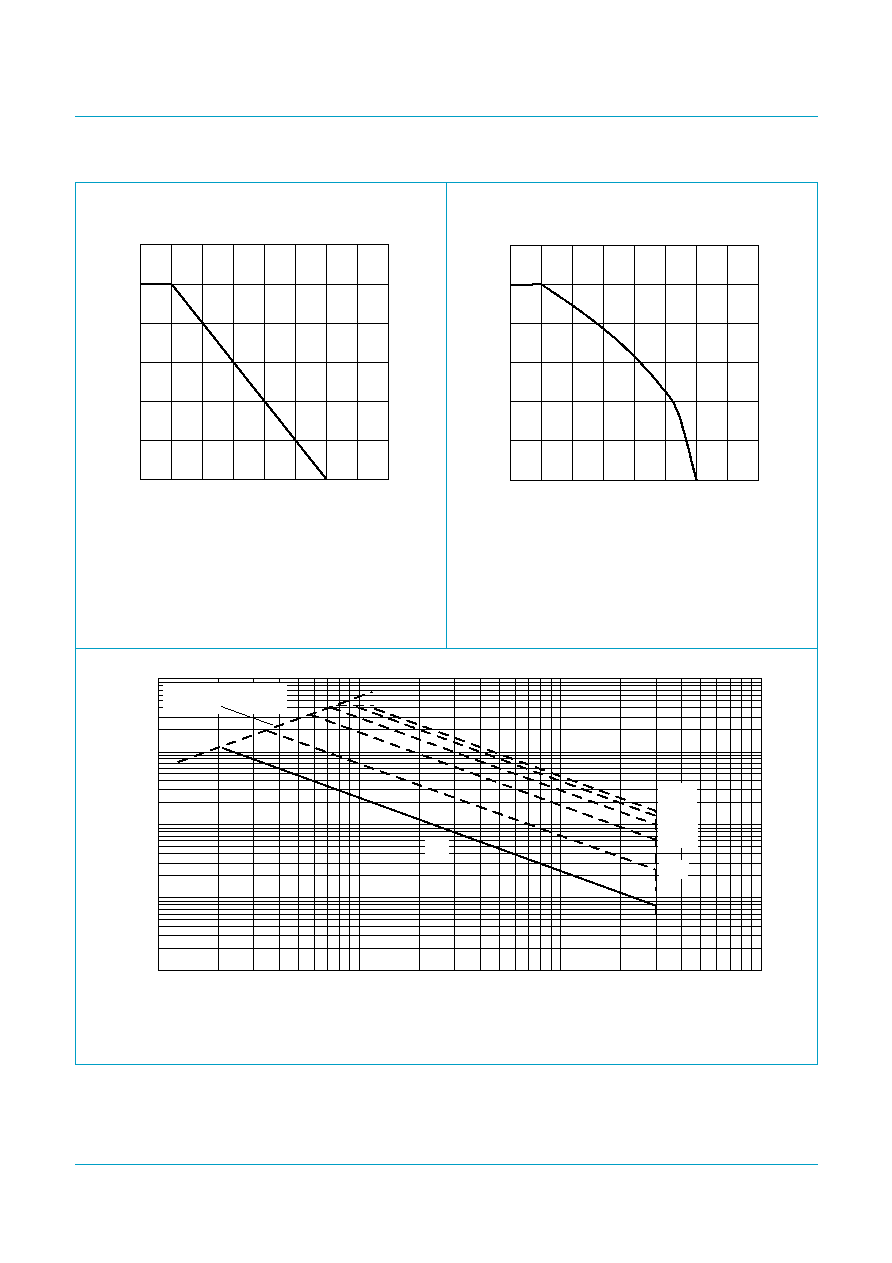
Fig 1.
Normalized total power dissipation as a
function of solder point temperature.
Fig 2.
Normalized continuous drain current as a
function of solder point temperature.
T
sp
= 25
∞
C; I
DM
is single pulse
Fig 3.
Safe operating area; continuous and peak drain currents as a function of drain-source voltage.
03aa17
0
40
80
Pder
120
0
50
100
150
200
Tsp (∫C)
(%)
03aa25
0
40
80
120
0
50
100
150
200
Tsp
(
o
C)
Ider
(%)
P
der
P
tot
P
tot 25 C
∞
(
)
-----------------------
100%
◊
=
I
der
I
D
I
D 25 C
∞
(
)
-------------------
100%
◊
=
Limit RDSon = VDS / ID
DC
tp =
100
µ
s
1 ms
10 ms
VDS (V)
102
10
1
10-1
ID
(A)
102
10
10-1
1
10-2
003aaa160
10
µ
s
1 s

Philips Semiconductors
SI4884
TrenchMOSTM logic level FET
Product data
Rev. 02 -- 12 April 2002
4 of 12
9397 750 09582
© Koninklijke Philips Electronics N.V. 2002. All rights reserved.
4.
Thermal characteristics
4.1 Transient thermal impedance
Table 3:
Thermal characteristics
Symbol Parameter
Conditions
Min
Typ
Max
Unit
R
th(j-a)
thermal resistance from junction to ambient mounted on a printed circuit board;
t
p
10 s; minimum footprint;
Figure 4
-
60
-
K/W
Fig 4.
Transient thermal impedance from junction to ambient as a function of pulse duration.
102
Zth(j-a)
(K/W)
10
1
102
10
1
10-1
10-2
10-3
10-4
tp (s)
single pulse
0.02
0.05
= 0.5
0.2
0.1
003aaa161
tp
tp
T
P
t
T
=

Philips Semiconductors
SI4884
TrenchMOSTM logic level FET
Product data
Rev. 02 -- 12 April 2002
5 of 12
9397 750 09582
© Koninklijke Philips Electronics N.V. 2002. All rights reserved.
5.
Characteristics
Table 4:
Characteristics
T
j
= 25
∞
C unless otherwise specified
Symbol Parameter
Conditions
Min
Typ
Max
Unit
Static characteristics
V
(BR)DSS
drain-source breakdown voltage
I
D
= 250
µ
A; V
GS
= 0 V
30
-
-
V
V
GS(th)
gate-source threshold voltage
I
D
= 250
µ
A; V
DS
= V
GS
;
Figure 9
1
-
2
V
I
DSS
drain-source leakage current
V
DS
= 24 V; V
GS
= 0 V
T
j
= 25
∞
C
-
-
1
µ
A
T
j
= 100
∞
C
-
-
5
µ
A
I
GSS
gate-source leakage current
V
GS
=
±
20 V; V
DS
= 0 V
-
100
nA
R
DSon
drain-source on-state resistance
V
GS
= 4.5 V; I
D
= 10 A;
Figure 7
and
8
-
11
16.5
m
V
GS
= 10 V; I
D
= 12 A;
-
8.9
10.5
m
Dynamic characteristics
g
fs
forward transconductance
V
DS
= 15 V; I
D
= 10 A;
-
34
-
S
Q
g(tot)
total gate charge
I
D
= 15 A; V
DD
= 16 V; V
GS
= 5 V;
Figure 13
-
17.6
-
nC
Q
gs
gate-source charge
-
4
-
nC
Q
gd
gate-drain (Miller) charge
-
4.4
-
nC
C
iss
input capacitance
V
GS
= 0 V; V
DS
= 16 V; f = 1 MHz;
Figure 11
-
1335 -
pF
C
oss
output capacitance
-
391
-
pF
C
rss
reverse transfer capacitance
-
190
-
pF
t
d(on)
turn-on delay time
V
DD
= 16 V; R
D
= 10
; V
GS
= 10 V
-
10.6
-
ns
t
r
rise time
-
11.7
-
ns
t
d(off)
turn-off delay time
-
37
-
ns
t
f
fall time
-
19
-
ns
Source-drain (reverse) diode
V
SD
source-drain (diode forward) voltage I
S
= 1 A; V
GS
= 0 V;
Figure 12
-
0.7
1.0
V
t
rr
reverse recovery time
I
S
= 2.3 A; dI
S
/dt =
-
100 A/
µ
s; V
GS
= 0 V
-
70
-
ns