 | –≠–ª–µ–∫—Ç—Ä–æ–Ω–Ω—ã–π –∫–æ–º–ø–æ–Ω–µ–Ω—Ç: TDA1315H | –°–∫–∞—á–∞—Ç—å:  PDF PDF  ZIP ZIP |

DATA SHEET
Product specification
Supersedes data of December 1994
File under Integrated Circuits, IC01
1995 Jul 17
INTEGRATED CIRCUITS
TDA1315H
Digital audio input/output circuit
(DAIO)

1995 Jul 17
2
Philips Semiconductors
Product specification
Digital audio input/output circuit (DAIO)
TDA1315H
FEATURES
∑
Transceiver for SPDIF and
"IEC 958" encoded signals
∑
High sensitivity input for transformer-coupled links
∑
TTL-level input for optical links
∑
Built-in IEC input selector
∑
Built-in IEC feed-through function
∑
Automatic sample frequency (f
s
) detection
∑
System clock recovery from IEC input signal
∑
Low system clock drift when IEC input signal is removed
∑
Error detection and concealment
∑
PLL lock detection in transmit mode
∑
Serial audio interface conforms to I
2
S-bus format
∑
Auxiliary I
2
S-bus input for Analog-to-Digital Converter
(ADC)
∑
Audio output selector
∑
Microcontroller-controlled and stand-alone mode
∑
128-byte buffer for user data
∑
Bytewise exchange of user data with microcontroller
∑
Decoding of Compact Disc (CD) subcode Q-channel
data
∑
Support for serial copy management system (SCMS)
∑
Light Emitting Diode (LED) drive capability
(sample frequency and error indication)
∑
Pin-selectable device address for
microcontroller interface
∑
Power-down mode.
GENERAL DESCRIPTION
The Digital Audio Input/Output circuit (DAIO) of the
TDA1315H is a complete transceiver for biphase-mark
encoded digital audio signals that conform to the SPDIF
and
"IEC 958" interface standards (consumer mode),
made in the full CMOS-process C200.
In the receive mode, the device adjusts automatically to
one of the three standardized sample frequencies
(32, 44.1 or 48 kHz), decodes the input signal and
separates audio and control data. A clock signal of either
256 or 384 times the sample frequency is generated to
serve as a master clock signal in digital audio systems.
In the transmit mode, the device multiplexes the audio
control and user data and encodes it for subsequent
transmission via a cable or optical link.
ORDERING INFORMATION
TYPE
NUMBER
PACKAGE
NAME
PIN POSITION
VERSION
TDA1315H
QFP44
plastic quad flat package; 44 leads (lead length 1.3 mm);
body 10
◊
10
◊
1.75 mm
SOT307-2

1995 Jul 17
3
Philips Semiconductors
Product specification
Digital audio input/output circuit (DAIO)
TDA1315H
QUICK REFERENCE DATA
All inputs are TTL compatible; all outputs are CMOS compatible; unless otherwise specified.
SYMBOL
PARAMETER
CONDITIONS
MIN.
TYP.
MAX.
UNIT
Supply
V
DD
supply voltage
V
DDD
= V
DDA
3.4
5.0
5.5
V
I
DDAq
analog quiescent current
PD = 1; T
amb
= 25
∞
C
-
-
10
µ
A
I
DDDq
digital quiescent current
PD = 1; T
amb
= 25
∞
C
-
-
10
µ
A
I
DDA
analog supply current
f
s
= 48 kHz; CLKSEL = 0;
when IECIN1 input is used
-
2.6
-
mA
I
DDD
digital supply current
f
s
= 48 kHz; CLKSEL = 0
-
13
-
mA
Power
P
tot
total power dissipation
f
s
= 48 kHz; CLKSEL = 0;
when IECIN1 input is used
-
80
-
mW
Temperature
T
amb
operating ambient temperature
-
20
-
+70
∞
C
IEC interface; pin IECIN1 (high sensitivity IEC input)
V
i(p-p)
AC input voltage
(peak-to-peak value)
0.2
-
V
DD
V
Control part
CHMODE, UNLOCK, FS32, FS44, FS48
AND
COPY (
OPEN
-
DRAIN OUTPUTS
)
V
OL
LOW level output voltage
I
OL
= 3 mA
-
-
0.5
V
RESET, SCK, LCLK, LMODE
AND
SYSCLKI (
HYSTERESIS INPUTS
)
V
tHL
negative-going threshold
V
DD
= 4.5 to 5.5 V
0.6
-
-
V
V
tLH
positive-going threshold
V
DD
= 4.5 to 5.5 V
-
-
2.4
V
V
hys
input voltage hysteresis
V
DD
= 4.5 to 5.5 V
-
0.7
-
V
Clock and timing
V
ref
output reference voltage
-
2.1
-
V
RC
int
(
PIN
44)
I
CHfr
charge-pump output current
frequency detector loop
-
±
12
-
µ
A
I
CHph
charge-pump output current
phase detector loop
-
±
24
-
µ
A

1995 Jul 17
4
Philips Semiconductors
Product specification
Digital audio input/output circuit (DAIO)
TDA1315H
BLOCK DIAGRAM
Fig.1 Block diagram.

1995 Jul 17
5
Philips Semiconductors
Product specification
Digital audio input/output circuit (DAIO)
TDA1315H
PINNING
SYMBOL
PIN
PADCELL
DESCRIPTION
RC
fil
1
E029
PLL loop filter input
V
ref
2
E029
decoupling internal reference voltage output
V
DDA
3
E008
analog supply voltage
V
SSA
4
E004
analog ground
IECIN1
5
E007
high sensitivity IEC input
IECIN0
6
IPP04
TTL level IEC input
IECSEL
7
IUP04
select IEC input 0 or 1 (0 = IECIN0; 1 = IECIN1); this input has an internal pull-up
resistor
IECO
8
OPFH3
digital audio output for optical and transformer link
IECOEN
9
IUP04
digital audio output enable (0 = enabled; 1 = disabled/3-state); this input has an
internal pull-up resistor
TESTB
10
IPP04
enable factory test input (0 = normal application; 1 = scan mode)
TESTC
11
IPP04
enable factory test input (0 = normal application; 1 = observation outputs)
UNLOCK
12
OPP41A
PLL out-of-lock (0 = not locked; 1 = locked); this output can drive an LED
FS32
13
OPP41A
indicates sample frequency = 32 kHz (active LOW); this output can drive an LED
FS44
14
OPP41A
indicates sample frequency = 44.1 kHz (active LOW); this output can drive an LED
FS48
15
OPP41A
indicates sample frequency = 48 kHz (active LOW); this output can drive an LED
CHMODE
16
OPP41A
use of channel status block (0 = professional use; 1 = consumer use); this output
can drive an LED
V
DDD2
17
E008
digital supply voltage 2
V
SSD2
18
E009
digital ground 2
RESET
19
IDP09
initialization after power-on, requires only an external capacitor connected to V
DDD
;
this is a Schmitt-trigger input with an internal pull-down resistor
PD
20
IPP04
enable power-down input in the standby mode (0 = normal application; 1 = standby
mode)
CTRLMODE
21
IUP04
select microcontroller/stand-alone mode (0 = microcontroller; 1 = stand-alone); this
input has an internal pull-up resistor
LADDR
22
IPP04
microcontroller interface address switch input (0 = 000001; 1 = 000010)
LMODE
23
IPP09
microcontroller interface mode line input
LCLK
24
IPP09
microcontroller interface clock line input
LDATA
25
IOF24
microcontroller interface data line input/output
STROBE
26
IDP04
strobe for control register (active HIGH); this input has an internal pull-down resistor
UDAVAIL
27
OPF23
synchronization for output user data (0 = data available; 1 = no data)
TESTA
28
IPP04
enable factory (scan) test input (0 = normal application; 1 = test clock enable)
COPY
29
OPP41A
copyright status bit (0 = copyright asserted; 1 = no copyright asserted); this output
can drive an LED
INVALID
30
IOD24
validity of audio sample input/output (0 = valid sample; 1 = invalid sample); this pin
has an internal pull-down resistor
DEEM
31
OPF23
pre-emphasis output bit (0 = no pre-emphasis; 1 = pre-emphasis)
MUTE
32
IUP04
audio mute input (0 = permanent mute; 1 = mute on receive error); this pin has an
internal pull-up resistor

1995 Jul 17
6
Philips Semiconductors
Product specification
Digital audio input/output circuit (DAIO)
TDA1315H
I
2
SSEL
33
IUP04
select auxiliary input or normal input in transmit mode
SDAUX
34
IPP04
auxiliary serial data input; I
2
S-bus
SD
35
IOF24
serial audio data input/output; I
2
S-bus
WS
36
IOF24
word select input/output; I
2
S-bus
SCK
37
IOF29
serial audio clock input/output; I
2
S-bus
I
2
SOEN
38
IUP04
serial audio output enable (0 = enabled; 1 = disabled/3-state); this input has an
internal pull-up resistor
SYSCLKI
39
IPP09
system clock input (transmit mode)
SYSCLKO
40
OPFA3
system clock output (receive mode)
V
SSD1
41
E009
digital ground 1
V
DDD1
42
E008
digital supply voltage 1
CLKSEL
43
IUP04
select system clock (0 = 384f
s
; 1 = 256f
s
); this input has an internal pull-up resistor
RC
int
44
E029
integrating capacitor output
SYMBOL
PIN
PADCELL
DESCRIPTION
Fig.2 Pin configuration.

1995 Jul 17
7
Philips Semiconductors
Product specification
Digital audio input/output circuit (DAIO)
TDA1315H
FUNCTIONAL DESCRIPTION
Modes of operation
With respect to the control of the device and the exchange
of non-audio data, a microcontroller (host) mode and a
stand-alone mode can be considered. The selection of the
mode is performed at pin CTRLMODE.
In the stand-alone mode, the device configuration is solely
determined by pins. In the host mode an internal control
register, or pins or both can be used to change the default
settings.
With respect to the direction of the digital audio data, the
device can be operated in either a transmit or a receive
mode under control of a microcontroller. In the stand-alone
mode the device is only a receiver. In the receive mode the
input signal can also be made available at the output pin
IECO (feed-through) to ease the cascading of digital audio
equipment.
The device can be brought to standby mode at all times by
activating the PD pin (power down). In this mode all
functions are disabled, all outputs 3-stated, supply current
is minimized and the contents of the register are saved.
General
For those applications where it is important to save power,
the PD pin is provided, which, when activated, puts the
TDA1315H in standby mode by disabling all functions and
3-stating all outputs, while saving register contents.
As illustrated in Fig.1, the TDA1315H contains the
following major functional blocks:
∑
IEC input section
∑
Biphase demodulator
∑
Frame and error detection
∑
Clock and timing section
∑
IEC output section
∑
Biphase modulator
∑
Audio section (I
2
S-bus transceiver)
∑
Non-audio section (control and FIFO)
∑
User (microcontroller) interface.
IEC
INPUT SECTION
There are two biphase signal inputs to the IEC input
section. IECIN0 accepts TTL levels from, for example, an
optical input device, while IECIN1 is designed for coaxial
cable inputs and requires signal levels of minimum
200 mV (p-p) via an external coupling capacitor. The
selection of the active input channel is performed by pin
IECSEL or by the control register or both. In the receive
mode, the selected input signal is applied internally to the
biphase audio output section to enable a feed-through
function.
B
IPHASE DEMODULATOR
In the biphase demodulator, the received signal (for details
see Chapter "References"[1] and [2]) is converted to
binary data and separated into audio and non-audio data
for further processing in their dedicated sections. The
demodulated input signal is also required for frame and
error detection.
F
RAME AND ERROR DETECTION
In the frame and error detection block, the framing
information from the received biphase signal is retrieved to
synchronize the biphase demodulator and to allow access
to the audio and non-audio data bits. An out-of-lock
condition of the PLL is flagged at UNLOCK. The validity of
audio samples is indicated at pin INVALID.
C
LOCK AND TIMING SECTION
In the clock and timing section, the timing information
inherent to the received biphase signal is retrieved and a
symmetrical master clock signal is generated and output at
pin SYSCLKO. Depending on the mode of operation, the
frequency of this master clock can be selected by pin
CLKSEL, by the control register or both to be either 256f
s
or 384f
s
(f
s
= audio sampling frequency). This section
contains all the circuitry of a Phase-Locked Loop (PLL),
except for the loop filter components, which are connected
externally to pins RC
int
and RC
fil
. When the input signal is
interrupted, the oscillator will slowly drift to the
centre frequency in order to keep the system operating on
a proper frequency. In the transmit mode, all required
timing signals are input at pin SYSCLKI and are derived
from an externally supplied system clock of either 256f
s
or
384f
s
. The input HIGH time of that clock may be in the
range between 30% to 70% of the clock period.
IEC
OUTPUT SECTION
In the IEC output section, either the received (feed-through
function) or the generated biphase signal is selected for
output at pin IECO, depending on the receive/transmit
mode. The output can be enabled/disabled by pin
IECOEN, by the control register or both, and can drive a
suitable optocoupler and a transformer in parallel.

1995 Jul 17
8
Philips Semiconductors
Product specification
Digital audio input/output circuit (DAIO)
TDA1315H
B
IPHASE DEMODULATOR
In the biphase modulator section, audio and non-audio
data are combined into subframes, frames and blocks, and
encoded in the biphase-mark format during transmit mode.
Although there are always 24 audio bits per sample in a
subframe, the number of significant bits can be selected as
16, 18, 20 or 24 via the control register (host mode).
A
UDIO SECTION
In the audio section, the left and right channel audio
samples are taken from the demodulated data frames and
are output serially in accordance with the I
2
S-bus format
(for details see Chapter "References"[3] pins SD, SCK and
WS) when the TDA1315H is in the receive mode (I
2
S-bus
transmitter). The audio output signals are concealed or
muted in case certain errors were detected during
reception. Mute can be enforced by pin MUTE or via the
control register (host mode) and affects, depending on the
receive/transmit mode, the I
2
S-bus or IEC output signals.
MUTE is internally synchronized with the audio data. In the
transmit mode, there is an additional I
2
S-bus data input
SDAUX made available to accept audio data from, for
example, an ADC. This input can be selected either by pin
I
2
SSEL, by the control register or both. The I
2
S-bus Port
can be enabled/disabled by pin I
2
SOEN, by the control
register or both. In the transmit mode, I
2
S-bus data and
timing are supplied by an external source, the TDA1315H
then becomes an I
2
S-bus receiver. In this event, selection
of an I
2
S-bus source determines which signal is to be
output at IECO. Although the phase relationship between
system clock (SYSCLKI) and I
2
S timing (SCK) is not
critical they must be synchronous with each other, i.e. be
derived from the same source.
Receive mode
The IEC subframe format defines 20 bits for an audio
sample, plus 4 auxiliary bits, which can be used to extend
the word length. By default, all 24 data bits per sample are
output via the I
2
S-bus Port. This can be changed,
however, to 16, 18 or 20 bits via bits 2 and 3 in byte 1 of
the control register. The remaining bits will then be zero.
The serial audio clock frequency at pin SCK is 64
◊
f
s
, i.e.
there are 32 clock pulses per audio sample (left or right
channel).
Apart from detecting the out-of-lock condition of the PLL,
received data is checked for the errors listed below. All
detected errors will be flagged in the status register and
two of them brought out to a pin. Depending on the type of
error, different measures are taken.
∑
Validity flag set. This error condition is also output at pin
INVALID, simultaneously with the data. The
corresponding audio sample is not modified.
∑
Parity check error. A concealment operation is
performed on both audio channels (left and right), i.e.
the last correctly received stereo sample is output again.
∑
Biphase violation (other than preambles). A
concealment operation (hold) is performed on both
audio channels (left and right), i.e. the last correctly
received stereo sample is output again.
∑
PLL is out-of-lock. This error condition is also output at
pin UNLOCK. Both audio output channels (left and right)
are set to zero (mute). The error condition is sampled
with the HIGH-to-LOW transition of WS, i.e. muting
becomes effective when the outputting of a stereo
sample begins. When the PLL has locked again, muting
is released only after a full block of audio samples has
been received, free of errors.The INVALID output will
always be set to LOW simultaneously with this muting.
In the receive mode it is possible to select the auxiliary
I
2
S-bus data input SDAUX for output at pin SD. However,
there will be no suitable system clock available in the event
of an open IEC input or a disabled IEC source and output
SD will be muted when the TDA1315H is not in lock.
Regardless of which source is selected, a MUTE
command will always mute the output signal at pin SD and
set the INVALID output to LOW regardless of the validity
bit value. When mute command is disabled, muting will be
released when the outputting of the next stereo sample
begins.

1995 Jul 17
9
Philips Semiconductors
Product specification
Digital audio input/output circuit (DAIO)
TDA1315H
Table 1
Summary of validity and muting in the receive mode
Note
1. X = don't care.
INPUT CONDITIONS
(1)
OUTPUTS
PLL LOCKED
MUTE
ACTIVATED
SDAUX
SELECTED
I
2
SOUT
ENABLED
VALIDITY BIT
INVALID
SD
X
X
X
no
X
3-state
3-state
No
X
X
yes
X
0
0
X
yes
X
yes
X
0
0
Yes
no
no
yes
0
0
IEC
Yes
no
no
yes
1
1
IEC
Yes
no
yes
yes
X
0
SDAUX
When the I
2
S-bus output Port is disabled by pin I
2
SOEN in
the stand-alone mode, pins WS, SCK, SD and INVALID
will immediately become 3-state. If, however, this is
performed in the host mode via the I
2
SOEN pin or the
corresponding bit in the control register, only SD and
INVALID will become 3-state immediately. Pins WS and
SCK will only become 3-state after the rising edge of
STROBE when the STROBE pulse changes the setting
from receive to transmit mode. Thus in the host mode,
when remaining in the receive mode, I
2
SOEN only
influences the SD and INVALID pins. Pins WS and SCK
are always enabled. When the I
2
S-bus output Port is
re-enabled, data output will start with the beginning of a
new stereo sample.
Transmit mode
Although the IEC subframe format supports up to 24 bits
per audio sample, the number of significant bits can be
selected as 16, 18, 20 or 24 via the control register.
Because the I
2
S-bus Port then operates as a receiver, the
timing has to be selected so that all data bits can be
received. Any bits unused or unsupplied will be set to
logic 0.
The information regarding audio samples that may be
unreliable or invalid has to be entered at pin INVALID
simultaneously with the data input to pin SD. The timing
will be the same as in the CD decoder ICs (e.g. the EFAB
signal of the SAA7310, see Chapter "References"[5].
As the I
2
S-bus Port is used as an input, it must be disabled
by the correct combination of pin I
2
SOEN and the
corresponding bit in the control register. The pins WS and
SCK are set to 3-state on the rising edge of STROBE,
whenever the transmit mode is activated. I
2
SOEN
influences only the data pin SD. This allows for three
different configurations:
∑
Transmit mode #1, I
2
SOEN = 1, I
2
SSEL = 1. In this
instance, I
2
S-bus timing and data are derived from an
external source and entered at pins WS, SCK and SD.
Output will be at pin IECO, if IECOEN permits.
∑
Transmit mode #2, I
2
SOEN = 1, I
2
SSEL = 0. In this
instance, I
2
S-bus timing is derived from an external
source and entered at pins WS and SCK and is also
supplied to another I
2
S-bus source, such as an ADC.
Data from that other I
2
S-bus source is entered at pin
SDAUX. Output will be at pin IECO, if IECOEN permits.
In this instance, I
2
SSEL acts as a source selector for
pins SD and SDAUX.
∑
Transmit mode #3, I
2
SOEN = 0, I
2
SSEL = 0. In this
instance, I
2
S-bus timing is derived from an external
source and entered at pins WS and SCK and is also
supplied to another I
2
S-bus source, such as an ADC.
Data from the other I
2
S-bus source is entered at pin
SDAUX. Output will be at pin IECO, if IECOEN permits,
and at pin SD. In this mode, SDAUX data is available
both at the IEC output (a type of digital monitor function)
and on the I
2
S-bus (e.g. for digital signal processing
purposes).
The remaining combination (I
2
SOEN = 0, I
2
SSEL = 1) is
not used. WS, SCK and SD are then 3-state.
Because the SDAUX input normally receives a signal from
an ADC, the signal at pin INVALID will not be interpreted
when this input is selected. All samples are assumed to be
valid. In all transmit modes, INVALID is an input pin.

1995 Jul 17
10
Philips Semiconductors
Product specification
Digital audio input/output circuit (DAIO)
TDA1315H
Whenever MUTE is activated in any of the transmit modes, the audio data of the IEC output signal will be muted and the
validity bit set to logic 0, regardless of the INVALID input value. When SDAUX is selected, MUTE will also affect the
output at pin SD.
Table 2
Summary of validity and muting in the transmit mode
Note
1. X = don't care.
INPUT CONDITIONS
(1)
IEC OUTPUT SIGNAL
MUTE ACTIVATED
SDAUX SELECTED
INVALID INPUT
VALIDITY BIT
AUDIO BITS
No
no
0
0
from SD
No
no
1
1
from SD
No
yes
X
0
from SDAUX
Yes
X
X
0
0
N
ON
-
AUDIO SECTION
In the non-audio section, the first 30 channel status bits
are taken from each block of data. A selection of 16 bits is
then assembled as two bytes and transferred to the user
interface. In the event of an incorrect IEC signal, i.e. no
consumer mode, an error will be flagged at pin CHMODE.
The error signal will return to its passive state after a full
block of consumer mode data has been received. The user
data bits are searched for the beginning of a `message'
(see Section "User data"), which is then stored bytewise in
a buffer that can be read by an external microcontroller via
the user interface. In the transmit mode, channel status
and user data bits are taken from an internal buffer that
has been written to by an external microcontroller via the
user interface. These bits are required for frame
composition in the biphase modulator.
The non-audio section supports only the consumer mode
of the
"IEC 958" specification and handles the channel
status and user data information.
The non-audio section can be operated in the stand-alone
mode (receive only) and the host mode (transmit/receive).
In the stand-alone mode, a few bits from the channel
status are brought out to pins, the user data is not
available. In the host mode, channel status and user data
are exchanged using a microcontroller. After a RESET in
the host mode, the TDA1315H provides general format by
default.
Channel status
The channel status consists of 30 bits, a number of which
are reserved for future standardization. The 16 most
significant bits (MSBs), arranged as two bytes, are
exchanged using an external microcontroller. The
mapping of the channel status bits into these two bytes is
given in Tables 3 and 4. All SCMS operations (Serial Copy
Management System) will be performed in the
microcontroller and no manipulation in the TDA1315H is
possible. Bit 0 is always the first bit on the user interface.
In the receive mode, an error signal is generated at pin
CHMODE if a professional mode signal is received. Even
then, two bytes of information, mapped as defined in
Tables 3 and 4, are generated for output. Although there
are two bytes of channel status available for output, only
the first byte can be read. To identify future modes of the
channel status, both mode bits (bits 6 and 7 in the channel
status) are available (inverted) from the TDA1315H status
register. The channel status is created from the left
channel subframes of the IEC signal (preambles `B'
and `M').
Whenever the channel status, as defined in
Tables 3 and 4 (16 bits), differs from the previously
received channel status, a bit will be set in the TDA1315H
status register. This helps to reduce the data traffic by
enabling the microcontroller to read the channel status
only after it has changed.
In the transmit mode, the microcontroller supplies
consumer mode (Mode 0) channel status data as
described in Table 3. Both bytes need to be transferred.

1995 Jul 17
11
Philips Semiconductors
Product specification
Digital audio input/output circuit (DAIO)
TDA1315H
Table 3
First byte of transferred channel status
Table 4
Second byte of transferred channel status
User data
In principle, the user data bits may be used in any way
required by the user. In order to guarantee compatibility
between signals of any source, attempts have been made
for the standardization of a user data format. The basic
idea is to transfer `messages' that consist of `information
units'. As messages are, typically, asynchronous with the
IEC audio block structure, their transfer relies on software
protocol. Currently, the applications for CD subcode and
DAT have been accepted. Their general format complies
with that protocol and can be described as follows:
∑
User data is transferred in the form of messages.
∑
Messages consist of information units, i.e. groups of
8 bits (bytes).
∑
Messages are separated by more than 8 zero bits (0).
∑
Information units within a message may be separated by
0 up to and including 8 zero bits.
∑
The MSB of each byte is sent first in the user data
channel.
∑
The MSB of each byte is a 1-bit (1, start bit).
∑
For CD subcode, one byte consists of bits 1QRSTUVW.
BIT
DESCRIPTION
BIT IN
CHANNEL
STATUS
0 and 1
clock accuracy
29 and 28
2 and 3
sample frequency
25 and 24
4
pre-emphasis
3
5
copyright
2
6
audio/data
1
7
consumer/professional use
0
BIT
DESCRIPTION
BIT IN
CHANNEL
STATUS
0
category code
15
1
category code
14
2
category code
13
3
category code
12
4
category code
11
5
category code
10
6
category code
9
7
category code
8
Normally, the exchange of user data between the
TDA1315H and the microcontroller is based on the
general format described above. In the event of CD
subcode, this means that 96 bytes need to be transferred
for each subcode frame. In order to reduce the amount of
data traffic, it is possible to separate the Q-channel bits
from the user data and transfer only them. This mode can
be enabled by a bit in the control register and leads to the
transfers of only 12 bytes per subcode frame. As there is
no check in the TDA1315H whether user data is from a CD
source, this Q-channel decoding can be employed
whenever the user data format permits.
Receive mode
User data bits are extracted from the received IEC
subframes and searched for the beginning of a message.
When Q-channel decoding is disabled (in the control
register), the data bytes of a message are stored in a
buffer for subsequent external interpretation or
processing. Any 0 bits between information units and
between messages are skipped.
It is essential to maintain synchronization of messages,
even if not all bytes of a message can be exchanged with
the microcontroller in a single transfer, or if there are
several messages in the buffer. When user data is
transferred in the general format described earlier, the
beginning of a message is indicated in the buffer by a 1 bit
in the MSB position of the first byte of that message. In all
subsequent bytes of the same message, the MSB will be
zero. This is illustrated in Table 5 for the CD subcode.
The user data buffer is implemented as a FIFO (First-In,
First-Out) with a size of 128 bytes. This allows the storing
of a full CD subcode frame. A synchronization signal at pin
UDAVAIL supports the transfer of user data to the
microcontroller. This signal goes LOW when there is at
least 1 byte of user data in the buffer, and returns HIGH
only after the last received byte has been read. This is
illustrated in Fig.3.
Based on the timing of the CD subcode, the
microcontroller should start reading data within 17 ms after
UDAVAIL has gone LOW, otherwise the buffer will fill
completely and the most recent data will be lost.

1995 Jul 17
12
Philips Semiconductors
Product specification
Digital audio input/output circuit (DAIO)
TDA1315H
Table 5
Synchronization of user data
MSB
USER DATA
LSB
FUNCTION
0
..
..
..
..
..
..
..
-
1
Q1
R1
S1
T1
U1
V1
W1
start of message
0
Q2
R2
S2
T2
U2
V2
W2
-
0
Q3
R3
S3
T3
U3
V3
W3
-
0
..
..
..
..
..
..
..
-
0
..
..
..
..
..
..
..
-
0
Q95
R95
S95
T95
U95
V95
W95
-
0
Q96
R96
S96
T96
U96
V96
W96
-
1
Q1
R1
S1
T1
U1
V1
W1
start of next message
0
Q2
R2
S2
T2
U2
V2
W2
-
0
Q3
R3
S3
T3
U3
V3
W3
-
0
..
..
..
..
..
..
..
-
Although the MSB is first within the IEC user data channel,
the LSB is sent first on the user interface to be compatible
with other data, i.e. the first byte of a subcode user data
frame will be output as follows:
1. Bit sent = W1.
2. Bit sent = V1.
3. Bit sent = U1.
4. Bit sent = T1.
5. Bit sent = S1.
6. Bit sent = R1.
7. Bit sent = Q1.
8. Bit sent = 1.
When Q-channel decoding is enabled, only the Q-channel
bits are taken from the user data frame and stored in the
buffer. Again, any separating 0 bits are skipped. Table 6
shows how data is arranged in the buffer.
Table 6
Layout of Q-channel data
MSB
USER DATA
LSB
..
..
..
..
..
..
..
..
Q89
Q90
Q91
Q92
Q93
Q94
Q95
Q96
Q1
Q2
Q3
Q4
Q5
Q6
Q7
Q8
Q9
Q10
Q11
Q12
Q13
Q14
Q15
Q16
Q17
Q18
Q19
Q20
Q21
Q22
Q23
Q24
..
..
..
..
..
..
..
..
..
..
..
..
..
..
..
..
Q89
Q90
Q91
Q92
Q93
Q94
Q95
Q96
Q1
Q2
Q3
Q4
Q5
Q6
Q7
Q8
..
..
..
..
..
..
..
..

1995 Jul 17
13
Philips Semiconductors
Product specification
Digital audio input/output circuit (DAIO)
TDA1315H
In this instance, synchronization of Q-channel frames must
be maintained by the microcontroller. It is recommended to
read decoded Q-channel data in groups of 12 bytes
otherwise synchronization of subcode frames may be lost
quickly. Again, the data transfer is supported by the signal
at pin UDAVAIL. This time it goes LOW when there is at
least one full frame (12 bytes) of Q-channel data in the
buffer, and goes HIGH again, when less than 12 bytes are
in the buffer. This is illustrated in Fig.4.
An initial synchronization can be obtained by clearing the
buffer via the control register, then start counting bytes
modulo 12. Again, the LSB is sent first on the user
interface, i.e. the first byte of a Q-channel frame will be
output as follows:
1. Bit sent = Q8.
2. Bit sent = Q7.
3. Bit sent = Q6.
4. Bit sent = Q5.
5. Bit sent = Q4.
6. Bit sent = Q3.
7. Bit sent = Q2.
8. Bit sent = Q1.
Writing to the buffer is disabled when the FIFO is full. It is
re-enabled when there is at least 1 byte free. Any data
overrun condition will be flagged as an error in the status
register. When this has occurred, the appropriate strategy
for data handling is decided by the microcontroller. It can,
for example, clear the buffer via the control register,
thereby discarding all remaining data, or it can start
reading data rapidly. Clearing the buffer turns UDAVAIL
HIGH. The response to reading data is the same as
described previously, depending on the mode of reception,
i.e. Q-channel decoding or normal message protocol.
For the period that the user data register is selected, the
microcontroller has to poll UDAVAIL each time after
reading one byte in normal mode, or 12 bytes in Q-channel
mode. Possible actions by the microcontroller are as
follows:
∑
If UDAVAIL = 0: reading the next byte in normal mode or
the next 12 bytes in Q-channel mode.
∑
If UDAVAIL = 1: either wait until UDAVAIL goes LOW
and continue reading user data byte(s), or write data,
read other data or deselect the TDA1315H by foreign
addressing.
≠ Remark: it is allowed to address the TDA1315H for
reading user data again when UDAVAIL is still HIGH,
but it is forbidden to apply clock pulses until UDAVAIL
has gone LOW.
Remark: whenever the buffer is empty (UDAVAIL = 1),
normally zeroes will be read, even when the
microcontroller tries to read more bytes. Doing so,
however, poses the risk of reading not all zeroes. In this
event new data is stored in the buffer during reading,
thereby losing synchronization. To assure correct
information will be read, the microcontroller should
perform an addressing sequence (not necessarily to the
TDA1315H), whenever an UDAVAIL HIGH is detected
before reading further.
Transmit mode
User data bits are supplied by the microcontroller in the
general message format only, Q-channel encoding is not
available in the TDA1315H. Again, UDAVAIL can be used
to synchronize transfers. It goes HIGH, when the buffer
contains at least 112 bytes, and goes LOW only when
there are no more than 16 bytes in the buffer. This is
illustrated in Fig.5.
Thus, after UDAVAIL has gone LOW, the microcontroller
can write a full CD subcode frame (96 data bytes plus
2 synchronization bytes) to the buffer without needing to
poll the state of pin UDAVAIL. In the event that no data are
available in the buffer, the user data bits in the IEC output
signal will be set to zero. Should the microcontroller
attempt to write more data than the buffer can hold, writing
will be disabled and the data overrun bit set in the status
register. Any bytes that have been transferred but not
written into the buffer are lost.
Four zero bits will be inserted automatically between user
data bytes (information units). The gap between
messages can be achieved by writing a single byte
containing all zeroes to the buffer.
U
SER INTERFACE
The user interface is an interface between the data
processing sections of the TDA1315H and the user. The
basic mode of operation (control by a host or stand-alone
operation) is selected by pin CTRLMODE. In the host
mode, all data, control and status information is, in
principle, exchanged with a microcontroller although the
device configuration can also be changed by pin control.
Up to 2 TDA1315Hs can be used on the same user
interface by setting different device addresses via the
LADDR pin. In the stand-alone mode (receive only), no
microcontroller is needed because important information is
brought out to pins FS32, FS44 and FS48, being an
indication of sample frequency, copyright protection
(COPY) (see Chapter "References"[2]) and use of
pre-emphasis (DEEM).

1995 Jul 17
14
Philips Semiconductors
Product specification
Digital audio input/output circuit (DAIO)
TDA1315H
Stand-alone mode
In this mode, the TDA1315H is automatically configured as
a receiver. The configuration, i.e., the mode of operation of
the device, is determined by pins CTRLMODE, IECSEL,
IECOEN, CLKSEL, I
2
SSEL and I
2
SOEN. Because all of
the pins have internal pull-up resistors, the default
configuration can be changed by pulling a pin LOW.
The output signals listed below are provided from the
channel status. However, all of them are switched off when
the PLL is not locked. This includes the situation where no
IEC input signal is available:
∑
Sample frequency is 32 kHz (pin FS32)
∑
Sample frequency is 44.1 kHz (pin FS44)
∑
Sample frequency is 48 kHz (pin FS48)
∑
Copyright status bit (pin COPY)
∑
Pre-emphasis bit (pin DEEM).
As there will be no output signals from the channel status
in the event that non-consumer IEC signals are received,
the I
2
S-bus output will still output data in 24 bits format. An
LED can be connected to pin CHMODE to provide an
indication of such a situation.
Host mode
In this mode, the exchange of data and control information
between the TDA1315H and a microcontroller is via a
serial hardware interface, which comprises the following
pins:
∑
LDATA to microcontroller interface data line.
∑
LCLK to microcontroller interface clock line.
∑
LMODE to microcontroller interface mode line.
∑
LADDR to microcontroller interface address switch.
Two different modes of operation can be distinguished:
1. Addressing mode.
2. Data transfer mode.
The addressing mode is used to select a device for
subsequent data transfer and to define the direction of that
transfer as well as the source or destination registers. The
addressing mode is characterized by LMODE being LOW
and a burst of 8 clock pulses at LCLK, accompanied by
8 data bits. The fundamental timing is illustrated in Fig.6.
Data bits 0 to 1 indicate the type of subsequent data
transfer as given in Table 7. The direction of the channel
status and user data transfers depends on the
transmit/receive mode.
Data bits 2 to 7 represent a 6-bit device address, with bit 7
being the MSB and bit 2 the LSB. The address of the
TDA1315H is 000001 (LADDR = 0) or 000010
(LADDR = 1). Should the TDA1315H receive a different
address, it will immediately 3-state the LDATA pin and
deselect its microcontroller interface logic. A dummy
address of 000000 is defined for the deselection of all
devices that are connected to the serial microcontroller
bus.
Fig.3 User data handshake.

1995 Jul 17
15
Philips Semiconductors
Product specification
Digital audio input/output circuit (DAIO)
TDA1315H
Fig.4 Q-channel handshake.
Fig.5 Transmit mode handshake.
Fig.6 Addressing mode timing.

1995 Jul 17
16
Philips Semiconductors
Product specification
Digital audio input/output circuit (DAIO)
TDA1315H
Table 7
Selection of data exchange
In the data transfer mode, the microcontroller exchanges data with the TDA1315H after it has addressed the device and
defined the type of data for that exchange. The selection remains active until the TDA1315H receives a new type of data
or is deselected. The fundamental timing of data transfers is illustrated in Fig.7, where LDATA denotes the data from the
TDA1315H to the microcontroller (LDATA read). The timing for the opposite direction is essentially the same as in the
addressing mode (LDATA write).
BIT 1
BIT 0
TRANSFER
DIRECTION
0
0
channel status
input/output
0
1
user data
input/output
1
0
control
input
1
1
status
output
Fig.7 Data transfer mode timing.
All transfers are bytewise, i.e. they are based on groups of
8 bits. Data will be stored in the TDA1315H after the eighth
bit of each byte has been received. It is possible to read
only the first byte of the channel status and of the
TDA1315H status register.
A multi-byte transfer is illustrated in Fig.8. As some other
devices, which are expected to connect to the same
microcontroller bus lines, require an indication of when
8 bits have been transferred, a so-called halt mode has
been defined. It is characterized by the following
conditions: LMODE = LOW, LDATA = 3-state and
LCLK = HIGH. The TDA1315H does not need this mode to
distinguish one byte from the next, however, it will not
make any difference when this occurs. When not used,
there is no need to increase the time between the last
LCLK pulse of a byte and the first LCLK pulse of the next
byte.

1995 Jul 17
17
Philips Semiconductors
Product specification
Digital audio input/output circuit (DAIO)
TDA1315H
Fig.8 Multi-byte transfer.
DAIO control
Under microcontroller control, there is also a transmit
mode available. Therefore, setting the device
configuration is slightly different from the stand-alone
mode. Most functions or modes can be set by pins or by
the control register or by both. Negative logic is used to
implement this `OR' function. The initial setting of the
control register is all ones. For most functions, the
TDA1315H can be configured only by pins, as explained
for the stand-alone mode. The principle of this type of
control is illustrated in Fig.9. However, for changing
CLKSEL, I
2
SSEL and the receive/transmit mode, there is
a configuration register, which is updated only by an
externally supplied STROBE signal. This allows
synchronization with other ICs.
At pin LDATA, control information is first entered serially
into a shift register and then latched in the control register
when complete. The bits of the second byte (6 are used)
of this register are internally ORed with their
corresponding pins, so that either a LOW or a logic 0 bit
will result in a logic 0 state (active LOW). These combined
states are then entered in the status register. The resulting
CLKSEL and I
2
SSEL information is supplied to the
configuration register, i.e. these bits will only be executed
in the TDA1315H, together with the receive/transmit bit,
after a STROBE has been received. This applies to the
host mode. In the stand-alone mode, the configuration
register is transparent and any configuration changes are
executed immediately. When the TDA1315H status is
read, the contents of the status register are output serially
at pin LDATA, thereby reflecting the `OR' combination of
configuration control bits and associated pins (negative
logic). The microcontroller is thereby able to determine
whether a pin is open-circuit or tied to ground.
When a STROBE is applied in the receive mode (to switch
to transmit mode), the outputs WS and SCK are disabled
one or two system clock periods after the rising edge of
STROBE. At the same time SYSCLKO will be forced LOW
and will be disabled one system clock later.
In the transmit mode it is possible to set the
receive/transmit bit to zero and then poll the locking status
of the TDA1315H and wait with a STROBE until the
TDA1315H is in-lock. This method can be used to check
whether there is an IEC source, since the TDA1315H will
not lock without one. It should be noted that the locking
status bit and the UNLOCK pin are only valid, i.e. its value
has a meaning, when you are in either the receive mode or
the receive/transmit bit is set to zero in the transmit mode.
When the configuration is changed to the receive mode,
WS, SCK, INVALID and SYSCLKO outputs are enabled
one or two system clock periods after the falling edge of
STROBE. SYSCLKO will always be initially LOW, for a
short time, and then pulses will appear always starting with
the rising edge.
In general WS and SCK outputs are always
enabled/disabled simultaneously. Output INVALID will
only be enabled when SD, WS and SCK are all enabled.
The mode timing is illustrated in Fig.10.
The control register consists of two bytes. The meaning of
the control register bits is given in Tables 8 and 9. All bits
default to a logic HIGH state after a reset to the
TDA1315H. This requires a reset for proper initialization
when CTRLMODE is changed after power-up. The LSB
(bit 0) is always transferred first.

1995 Jul 17
18
Philips Semiconductors
Product specification
Digital audio input/output circuit (DAIO)
TDA1315H
Fig.9 Mode control.
Table 8
First byte of control register
Note
1. Bit 4 is reset to HIGH after the TDA1315H has cleared
the buffer and has either caused UDAVAIL to go HIGH
in the receive mode or LOW in the transmit mode.
BIT
DESCRIPTION
FUNCTION
0
transmit/receive mode
0 = receive
1 = transmit
1
decode subcode
Q-channel
0 = enable
1 = disable
3 and 2
number of bits to
transfer
00 = 16 bits
01 = 18 bits
10 = 20 bits
11 = 24 bits
4
(1)
clear user data buffer
0 = clear
1 = leave as is
5
reserved
0 = undefined
1 = default
6
reserved
0 = undefined
1 = default
7
reserved
0 = undefined
1 = default
Table 9
Second byte of control register
BIT
DESCRIPTION
FUNCTION
0
audio mute
0 = enabled
1 = disabled
1
IEC output enable
0 = enabled
1 = disabled
2
select IEC input
0 = TTL level
1 = high sensitivity
3
I
2
S-bus output enable
0 = enabled
1 = disabled
4
select I
2
S-bus source
0 = SDAUX
1 = SD
5
select clock frequency
0 = 384f
s
1 = 256f
s
6
reserved
0 = undefined
1 = default
7
reserved
0 = undefined
1 = default

1995 Jul 17
19
Philips Semiconductors
Product specification
Digital audio input/output circuit (DAIO)
TDA1315H
Fig.10 Mode switching and timing STROBE input.

1995 Jul 17
20
Philips Semiconductors
Product specification
Digital audio input/output circuit (DAIO)
TDA1315H
Status
The status register consists of two bytes. A description of
the status register bits is given in Tables 10 and 11. After
a reset all bits in the status register will be one.
The various error conditions of the TDA1315H are
reflected in bits 0 to 6 of the first byte. The error bits are set
(LOW) when the corresponding error conditions occur,
they are reset (HIGH) only after the register has been read
by the microcontroller. Bit 7 reflects the active
transmit/receive state. It is updated after the TDA1315H
configuration, as determined by bit 0 of the first control
register byte, has been changed. This allows verification of
the mode change to, for example, release a mute signal
after a successful change.
Table 10 First byte of status register
BIT
DESCRIPTION
FUNCTION
0
channel status mode
0 = professional
1 = consumer
1
PLL lock condition
0 = not locked
1 = locked
2
validity flag
0 = error
1 = no error
3
parity check
0 = error
1 = no error
4
biphase violation
0 = error
1 = no error
5
user data overrun
0 = error
1 = no error
6
channel status check
0 = change
1 = no change
7
direction of data
0 = receive
1 = transmit
Table 11 Second byte of status register
Note
1. Bits 6 and 7 in the second byte of the status register
contain the inversion of bits 7 and 6, respectively, of
the channel status, which are used as mode bits.
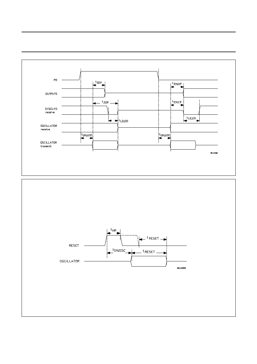
Reset and standby mode
Figure 11 illustrates the timing for the toggling between
normal and standby mode.
In Figs 11 and 12, when activating PD or RESET, 0 ns can
be taken for t
ON:OSC
when the oscillator is running (e.g.
receive mode).
The TDA1315H uses its internal oscillator for the reset and
standby function. This means that it is not necessary, in
any mode, to apply a clock at the SYSCLKI input for the
TDA1315H to perform the reset or standby function.
For resetting the TDA1315H only a small pulse is
necessary at the RESET input. The device then
automatically starts the oscillator (in the event that it is not
running). The system will then do a synchronous reset
(internally) during approximately 3 internal clock periods.
This t
RESET
starts after the falling edge of RESET or when
the oscillator has started, whichever occurs last. Only
when this resetting has been accomplished will the
external pin programming (e.g. CLKSEL, I
2
SOEN etc.) be
read by the TDA1315H. The TDA1315H is then ready for
use.
BIT
DESCRIPTION
FUNCTION
0
audio mute
0 = enabled
1 = disabled
1
IEC output enable
0 = enabled
1 = disabled
2
select IEC input
0 = TTL level
1 = high sensitivity
3
I
2
S-bus output enable
0 = enabled
1 = disabled
4
select I
2
S-bus source
0 = SDAUX
1 = IEC or CD
5
select clock frequency
0 = 384f
s
1 = 256f
s
6
(1)
channel status (bit 7)
0 = bit 7 set
1 = bit 7 reset
7
(1)
inverse mode bit (bit 6)
0 = bit 6 set
1 = bit 6 reset
1995 Jul 17
21
Philips Semiconductors
Product specification
Digital audio input/output circuit (DAIO)
TDA1315H
Fig.11 Standby mode timing.
Fig.12 RESET timing.

1995 Jul 17
22
Philips Semiconductors
Product specification
Digital audio input/output circuit (DAIO)
TDA1315H
LIMITING VALUES
In accordance with the Absolute Maximum Rating System (IEC 134).
Notes
1. In all events and, also, when applied voltages are below
-
0.5 V or above V
DD
+ 0.5 V this current limitation should
be taken into account to prevent device damage.
2. Human body model: pins 25, 27, 30, 31 and 35 to 37 =
±
1500 V; R = 1.5 k
; C = 100 pF; 3 zaps positive and 3 zaps
negative.
3. Machine model: R = 25
; C = 200 pF; L = 0.5
µ
A; 3 zaps positive and 3 zaps negative.
HANDLING
Inputs and outputs are protected against electrostatic discharge in normal handling. However, to be totally safe, it is
desirable to take normal precautions appropriate to handling MOS devices.
THERMAL CHARACTERISTICS
SYMBOL
PARAMETER
CONDITIONS
MIN.
MAX.
UNIT
V
DD
supply voltage (pins 3, 17 and 42)
-
0.5
+6.5
V
I
DD
supply current per pin (pins 3, 17 and 42)
-
50
mA
V
all
voltage supplied to all pins
without current
limitations
-
0.5
V
DD
+ 0.5
V
I
I/O
input/output current on any pin
except supply pins and
pins 8, 12 to 16, 29 and 40
note 1
-
±
10
mA
I
I
input current pins 12 to 16 and 29
V
O
>
V
DD
+ 0.5 V;
output disabled; note 1
-
±
10
mA
I
I/O
input/output current pins 12 to 16 and 29
V
O
<
V
DD
+ 0.5 V;
note 1
-
±
20
mA
I
8
input/output current pin 8
note 1
-
±
60
mA
I
40
input/output current pin 40
note 1
-
±
80
mA
P
tot
total power dissipation
-
500
mW
T
stg
storage temperature
-
65
+150
∞
C
T
amb
operating ambient temperature
-
20
+70
∞
C
V
es
electrostatic handling
note 2
-
2000
+2000
V
note 3
-
200
+200
V
SYMBOL
PARAMETER
VALUE
UNIT
R
th j-a
thermal resistance from junction to ambient in free air
80
K/W

1995 Jul 17
23
Philips Semiconductors
Product specification
Digital audio input/output circuit (DAIO)
TDA1315H
CHARACTERISTICS
V
DDD1
= V
DDD2
= V
DDA
= 3.4 to 5.5 V; T
amb
-
20 to +70
∞
C; rise, fall, set-up and hold times are specified between 10%
and 90% of full amplitude; delays between 50%; times to and from 3-state with R
L
= 1.5 k
to
1
/
2
V
DD
; typical values are
valid at the typical supply voltage of 5 V unless otherwise specified.
SYMBOL
PARAMETER
CONDITIONS
MIN.
TYP.
MAX.
UNIT
Supply
V
DD
supply voltage
V
DDD
= V
DDA
3.4
5.0
5.5
V
I
DDD
digital supply current
PD = 1; T
amb
= 25
∞
C
-
-
10
µ
A
I
DDA
analog supply current
PD = 1; T
amb
= 25
∞
C
-
-
10
µ
A
T
HE FOLLOWING PARAMETERS ARE TYPICAL FOR RECEIVE MODE
;
ALL OUTPUTS ENABLED
(
NOT LOADED
); T
amb
= 25
∞
C;
V
DD
= 5 V
I
DDD
digital supply current
f
s
= 48 kHz; CLKSEL = 0
-
13
-
mA
I
DDA
analog supply current
f
s
= 48 kHz; CLKSEL = 0;
when IECIN1 input is used
-
2.6
-
mA
P
tot
total power dissipation
f
s
= 48 kHz; CLKSEL = 0;
when IECIN1 input is used
-
80
-
mW
TTL input switching levels (without Schmitt-trigger)
A
PPLICABLE TO PERIPHERAL TYPES
: IPP04, IUP04, IDP04, IOF24
AND
IOD24
V
IL
LOW level input voltage
V
DD
= 3.4 V
-
-
0.5
V
V
DD
= 4.5 V
-
-
0.8
V
V
DD
= 5.5 V
-
-
0.8
V
V
IH
HIGH level input voltage V
DD
= 3.4 V
1.5
-
-
V
V
DD
= 4.5 V
2.0
-
-
V
V
DD
= 5.5 V
2.0
-
-
V
TTL input thresholds (with Schmitt-trigger)
A
PPLICABLE TO PERIPHERAL TYPES
: IPP09, IDP09
AND
IOF29
V
tHL
negative-going threshold V
DD
= 3.4 V
0.3
-
-
V
V
DD
= 4.5 V
0.6
-
-
V
V
DD
= 5.5 V
0.6
-
-
V
V
tLH
positive-going threshold
V
DD
= 3.4 V
-
-
1.9
V
V
DD
= 4.5 V
-
-
2.4
V
V
DD
= 5.5 V
-
-
2.4
V
V
hys
hysteresis voltage
V
DD
= 3.4 V
-
0.6
-
V
V
DD
= 4.5 V
-
0.6
-
V
V
DD
= 5.5 V
-
0.8
-
V
Input pull-up and pull-down resistor values; note 1
A
PPLICABLE TO PERIPHERAL TYPES
: IUP04, IDP04, IDP09
AND
IOD24
R
pull
pull-up or pull-down
resistors
V
DD
= 3.4 V
32
-
203
k
V
DD
= 4.5 V
21
-
134
k
V
DD
= 5.5 V
17
-
104
k

1995 Jul 17
24
Philips Semiconductors
Product specification
Digital audio input/output circuit (DAIO)
TDA1315H
Outputs sink and source capabilities
A
PPLICABLE TO PERIPHERAL TYPES
: OPF23, IOF24, IOD24,
AND
IOF29 (2 mA
OUTPUTS
)
V
OL
LOW level output
voltage
V
DD
= 3.4 V; I
O
= 1.5 mA
-
-
0.5
V
V
DD
= 4.5 V; I
O
= 2 mA
-
-
0.5
V
V
DD
= 5.5 V; I
O
= 2.25 mA
-
-
0.5
V
V
OH
HIGH level output
voltage
V
DD
= 3.4 V; I
O
=
-
1.5 mA
2.9
-
-
V
V
DD
= 4.5 V; I
O
=
-
2 mA
4.0
-
-
V
V
DD
= 5.5 V; I
O
=
-
2.25 mA
5.0
-
-
V
A
PPLICABLE TO PERIPHERAL TYPE
: OPP41A (4 mA
OUTPUT
)
V
OL
LOW level output
voltage
V
DD
= 3.4 V; I
O
= 3 mA
-
-
0.5
V
V
DD
= 4.5 V; I
O
= 4 mA
-
-
0.5
V
V
DD
= 5.5 V; I
O
= 4.5 mA
-
-
0.5
V
A
PPLICABLE TO PERIPHERAL TYPE
: OPFH3 (12 mA
OUTPUT
)
V
OL
LOW level output
voltage
V
DD
= 3.4 V; I
O
= 9 mA
-
-
0.5
V
V
DD
= 4.5 V; I
O
= 12 mA
-
-
0.5
V
V
DD
= 5.5 V; I
O
= 13.5 mA
-
-
0.5
V
V
OH
HIGH level output
voltage
V
DD
= 3.4 V; I
O
=
-
9 mA
2.9
-
-
V
V
DD
= 4.5 V; I
O
=
-
12 mA
4.0
-
-
V
V
DD
= 5.5 V; I
O
=
-
13.5 mA
5.0
-
-
V
A
PPLICABLE TO PERIPHERAL TYPE
: OPFA3 (16 mA
OUTPUT
)
V
OL
LOW level output
voltage
V
DD
= 3.4 V; I
O
= 12 mA
-
-
0.5
V
V
DD
= 4.5 V; I
O
= 16 mA
-
-
0.5
V
V
DD
= 5.5 V; I
O
= 18 mA
-
-
0.5
V
V
OH
HIGH level output
voltage
V
DD
= 3.4 V; I
O
=
-
12 mA
2.9
-
-
V
V
DD
= 4.5 V; I
O
=
-
16 mA
4.0
-
-
V
V
DD
= 5.5 V; I
O
=
-
18 mA
5.0
-
-
V
Input and 3-state (OFF state) leakage currents
A
PPLICABLE TO PERIPHERAL TYPES
: IPP04
AND
IPP09
|
I
LI
|
input leakage current
V
I
= 0 or 5.5 V; V
DD
= 5.5 V
-
-
±
1
µ
A
A
PPLICABLE TO PERIPHERAL TYPES
: OPF23, OPFH3, OPFA3, OPP41A, IOF24
AND
IOF29
|
I
OZ
|
3-state leakage current
V
O
= 0 or 5.5 V;
V
DD
= 5.5 V
-
-
±
5
µ
A
IEC interface; note 2; (for timing see Chapter "References", item 1)
IECO (
PIN
8)
t
dIEC
output delay with
respect to IECINx
receive mode
2T
c
-
3T
c
+ 50
ns
SYMBOL
PARAMETER
CONDITIONS
MIN.
TYP.
MAX.
UNIT

1995 Jul 17
25
Philips Semiconductors
Product specification
Digital audio input/output circuit (DAIO)
TDA1315H
IECIN1 (
PIN
5)
V
i(p-p)
AC input voltage
(peak-to-peak value)
0.2
-
V
DD
V
I
i
input current
V
I
= 0 or 5 V; V
DD
= 5 V
-
±
550
-
µ
A
V
bias
DC bias voltage
-
0.5V
DD
-
V
I
2
S-bus interface; (for timing see Chapter "References", item 3)
SD
INPUT
/
OUTPUT
(
PIN
35)
t
dSDAUX
output delay with
respect to SDAUX
-
-
50
ns
Microcontroller interface (see Figs 6 and 7)
T
LCLK period
T
c
+ 50
-
-
ns
t
HC
LCLK HIGH period
25
-
-
ns
t
LC
LCLK LOW period
25
-
-
ns
t
SU;AD
LADDR set-up time
25
-
-
ns
t
HD;AD
LADDR hold time
25
-
-
ns
t
SU;MA
LMODE set-up time
addressing mode
1
/
2
(T
c
+ 50)
-
-
ns
t
HD;MA
LMODE hold time
addressing mode
1
/
2
(T
c
+ 50)
-
-
ns
t
SU;MT
LMODE set-up time
halt mode
25
-
-
ns
t
HD;MT
LMODE hold time
halt mode
25
-
-
ns
t
SU;DA
LDATA set-up time
write and addressing mode
25
-
-
ns
t
HD;DA
LDATA hold time
write and addressing mode
25
-
-
ns
t
EN;DT
LDATA enable time
data read mode
-
-
50
ns
t
HD;DT
LDATA hold time
data read mode; note 3
1
/
2
T
c
-
T
c
+ 50
ns
t
3DT
LDATA disable time
data read mode
-
-
50
ns
t
halt
LMODE halt time
0
-
-
ns
Mode switching and STROBE (see Fig.10)
t
H;SB
STROBE HIGH time
3T
c
+ 50
-
-
ns
t
L;SB
STROBE LOW time
3T
c
+ 50
-
-
ns
t
SU;SB
set-up time before
STROBE
for pins or bits
-
T
c
+ 50
-
-
ns
t
HD;SB
hold time after STROBE
for pins or bits
2T
c
+ 50
-
-
ns
t
DBIT
delay LCLK to internal
bit
control register
2T
c
-
3T
c
+ 50
ns
t
EN;SD
SD enable time
T
c
-
2T
c
+ 50
ns
t
3SD
SD and INVALID disable
time
-
-
T
c
+ 50
ns
t
EN;WS
WS, SCK and INVALID
enable time
T
c
-
2T
c
+ 50
ns
t
3WS
WS and SCK disable
time
T
c
-
2T
c
+ 50
ns
t
EN;CO
SYSCLKO enable time
T
c
-
2T
c
+ 50
ns
SYMBOL
PARAMETER
CONDITIONS
MIN.
TYP.
MAX.
UNIT

1995 Jul 17
26
Philips Semiconductors
Product specification
Digital audio input/output circuit (DAIO)
TDA1315H
t
3CO
SYSCLKO disable time
2T
c
-
3T
c
+ 50
ns
t
LE;CO
SYSCLKO LOW time
when enabled
1
/
2
T
s
-
1.5T
s
+ 50
ns
t
LD;CO
SYSCLKO LOW time
when disabled
T
c
-
T
s
-
T
c
+ 50
ns
t
HD;CI
SYSCLKI hold time
3T
c
+ 50
-
-
ns
t
ON;OSC
oscillator start-up time
C
ref
in
µ
F; note 4
0
-
1
/
10
C
ref
s
t
OFF;OSC
oscillator switch-off time
2T
c
-
3T
c
+ 50
ns
Standby mode (see Fig.11)
t
3OP
outputs disable time
-
-
T
c
+ 50
ns
t
EN;OP
outputs enable time
-
-
T
c
+ 50
ns
t
3CR
SYSCLKO disable time
receive mode
T
c
-
2T
c
+ 50
ns
t
EN;CR
SYSCLKO enable time
receive mode
-
-
T
c
+ 50
ns
RESET (see Fig.12)
t
HR
RESET HIGH time
25
-
-
ns
t
RESET
internal RESET time
-
-
2
µ
s
Clock and timing (pins SYSCLKI and SYSCLKO)
SYSCLKI
input clock duty factor
30
50
70
%
SYSCLKO
output clock duty factor
45
50
55
%
t/t
SYSCLKO output clock
jitter
V
DDA
<
10
µ
V
-
±
50
◊
10
-
6
-
k
oL
VCO conversion gain
RC
fil
to SYSCLKO;
CLKSEL = 1
-
225
◊
10
6
-
rad/s/V
k
oH
VCO conversion gain
RC
fil
to SYSCLKO;
CLKSEL = 0
-
250
◊
10
6
-
rad/s/V
2f
rL
VCO frequency tuning
range
at SYSCLKO; CLKSEL = 1
-
16
-
MHz
2f
rH
VCO frequency tuning
range
at SYSCLKO; CLKSEL = 0
-
22
-
MHz
f
cL
VCO centre frequency
at SYSCLKO; RC
fil
= V
ref
;
CLKSEL = 1
-
12.5
-
MHz
f
cH
VCO centre frequency
at SYSCLKO; RC
fil
= V
ref
;
CLKSEL = 0
-
19
-
MHz
V
ref
OUTPUT
(
PIN
2)
V
ref
output reference voltage
-
2.1
-
V
I
ref
output reference current
V
ref
= 0 V
-
28
-
µ
A
RC
fil
INPUT
(
PIN
1)
V
trL
input tuning voltage
f
s
= 32 to 48 kHz;
CLKSEL = 1
-
100
-
mV
V
trH
input tuning voltage
f
s
= 32 to 48 kHz;
CLKSEL = 0
-
150
-
mV
|
I
LI
|
input leakage current
V
I
= 0 or 5.5 V;
V
DD
= 5.5 V; TESTB = 1
-
-
±
1
µ
A
SYMBOL
PARAMETER
CONDITIONS
MIN.
TYP.
MAX.
UNIT

1995 Jul 17
27
Philips Semiconductors
Product specification
Digital audio input/output circuit (DAIO)
TDA1315H
Notes
1. Pull-up specified at input to V
SS
, pull-down specified at input to V
DD
.
2. Most timing specifications are related to clock periods. Two basic periods are of importance:
a) T
c
, this is the internal clock period of the TDA1315H being
1
/
128
f
s
seconds.
b) T
s
, this is the system clock period such as SYSCLKI or SYSCLKO, being
1
/
256
f
s
or
1
/
384
f
s
seconds.
c) It should be noted that in the receive mode clock frequencies are only reliable when the TDA1315H is in-lock.
3. In the transmit mode, when SYSCLKI is 384f
s
and 30% or 70% duty cycle: t
HD;DT
is 0.43T
c
minimum.
4. This time strongly depends on the external decoupling capacitor connected to V
ref
(pin 2). When the capacitor is
initially empty, it must first be charged before the oscillator can start.
5. Internally this resistor will be connected between RC
fil
and V
ref
, when there is no signal on the selected IEC input in
receive mode, or when the oscillator is turned off. This is to prevent the oscillator to drift to extreme low or high
frequencies. See also Chapter "Characteristics"with regards to f
oclk(l)
and f
oclk(u)
.
6. These figures are theoretical limits for the TDA1315H. In the application, the maximum frequencies at f
s
= 48 kHz
will be fixed. Consequently f
iclk
= 12.288 MHz (CLKSEL = 1) and f
iclk
= 18.432 MHz (CLKSEL = 0).
7. These frequencies mean that the TDA1315H is guaranteed to lock in the range f
s
= 31.5 to 48.5 kHz over the whole
supply voltage range and specified temperature range.
8. These are the limit frequencies that the internal oscillator may reach under extreme conditions when the VCO input
(pin RC
fil
) would be controlled far beyond its normal tuning range. An internal resistor however, prevents that these
frequencies can be reached when there is no signal to lock-on to. See also Chapter "Characteristics" regarding R
tr
.
QUALITY SPECIFICATION
In accordance with
"SNW-FQ-611E". The number of this quality specification can be found in the "Quality Reference
Pocketbook". The pocketbook can be ordered using the code 9398 510 34011.
R
tr
transmission-gate
resistor
V
ref
= 2.1 V; V
DD
= 5 V;
note 5
-
1
-
M
RC
int
OUTPUT
(
PIN
44)
C
o
parallel output
capacitance
-
5
-
pF
I
ch(fr)
output charge current
frequency detector loop
-
±
12
-
µ
A
I
ch(ph)
output charge current
phase detector loop
-
±
24
-
µ
A
SYSCLKI
INPUT
(
PIN
39);
TRANSMIT MODE
; V
DD
= 3.4
TO
5.5 V
f
iclk
input clock frequency
CLKSEL = 1; note 6
-
-
16
(6)
MHz
CLKSEL = 0; note 6
-
-
24
(6)
MHz
SYSCLKO
OUTPUT
(
PIN
40);
RECEIVE MODE
; V
DD
= 3.4
TO
5.5 V
f
oclk(l)
output clock frequency
lower limit oscillator
CLKSEL = 1
2
(8)
-
8.06
(7)
MHz
CLKSEL = 0
4
(8)
-
12.09
(7)
MHz
f
oclk(u)
output clock frequency
upper limit oscillator
CLKSEL = 1
12.42
(7)
-
26
(8)
MHz
CLKSEL = 0
18.63
(7)
-
37
(8)
MHz
SYMBOL
PARAMETER
CONDITIONS
MIN.
TYP.
MAX.
UNIT

1995 Jul 17
28
Philips Semiconductors
Product specification
Digital audio input/output circuit (DAIO)
TDA1315H
TEST AND APPLICATION INFORMATION
Figures 13 to 15 indicate typical systems environment of the TDA1315H. They are intended to give examples of which
external blocks may be added to compose a system for particular requirements. The loop filter configuration and values
in the examples meet the requirements for mid-end and high-end audio applications.
Test information
Table 12 Test pin functions
Table 13 Implemented test scan chains
TEST PIN
DESCRIPTION
TESTA = 0
normal application operation
TESTA = 1
test mode i.e. system clock equals SYSCLKI
TESTB = 0
normal mode when TESTA = 1
TESTB = 1
scan mode when TESTA = 1; high-ohmic resistor between RC
fil
and V
ref
pins always disabled
TESTC = 0
normal operation
TESTC = 1
CHMODE equals system clock; IECO equals IECIN1 slicer output; RAM test enabled
SCAN NUMBER
LENGTH (BITS)
SCAN INPUT
OUTPUT
ACTIVE EDGE OF
SYSCLKI
1
54
IECSEL
FS32
negative
2
54
IECOEN
FS44
negative
3
54
LADDR
FS48
negative
4
54
MUTE
COPY
negative
5
53
LMODE
CHMODE
negative
6
53
STROBE
UDAVAIL
negative
7
51
I
2
SSEL
DEEM
negative
8
31
CLKSEL
UNLOCK
positive

1995 Jul 17
29
Philips Semiconductors
Product specification
Digital audio input/output circuit (DAIO)
TDA1315H
Stand alone application (receive only)
A very simple implementation of the stand-alone
application is illustrated in Fig.13. In simple terms, it is an
IEC-to-analog converter. The IEC signal is input via a
shielded cable and enters the TDA1315H via its
high-sensitivity input. The audio output is supplied to a
DAC via the enabled I
2
S-bus Port, the DEEM output can
be used to switch a de-emphasis network in and out of the
signal path. The system clock frequency can be selected
and is available should any digital filters in the DAC block
require such a clock. The sample frequency of the
received signal together with any out-of-lock condition of
the phase-locked loop and the presence of a professional
mode IEC signal can be displayed with LEDs.
Fig.13 Simple stand-alone application.
When in a system both IECIN1 and IECIN0 inputs are used, the signal that is applied to the IECIN0 input must be kept away from the IECIN1 input on
the printed-circuit board. Steep slopes of the IECIN0 input can be seen by the sensitive adjacent IECIN1 input. An extra capacitance parallel to the 75
resistor, close to the TDA1315H, can help reduce the crosstalk if required. A suitable value is 180 pF.

1995 Jul 17
30
Philips Semiconductors
Product specification
Digital audio input/output circuit (DAIO)
TDA1315H
Microcontroller based application (receive and/or
transmit)
The microcontroller-based application is illustrated in
Fig.14. Functional blocks are shown for both the receive
and the transmit mode. Here, the IEC signal is input via an
optical fiber link and an associated optocoupler and enters
the TDA1315H at its TTL-level input. The I
2
S-bus output
signal is applied to a digital signal processing module,
which may contain signal processors, DACs, a recording
device etc. An ADC can be an optional source for that
module. As the microcontroller can obtain all status
information and data via the serial bus, it will provide
display information and also will control the whole system,
including the receive/transmit switch. For simplicity
reasons, pin-based mode selection is not shown in this
diagram. In the transmit mode, both system clock and
I
2
S-bus timing are derived from a central timing block. The
IEC output signal feeds an optical fiber link via a suitable
optocoupler.
Concerning the wide supply voltage range of the
TDA1315H, it is not possible to have a
transformer-coupled IEC output that fulfils the
"IEC 958"
standard over the full supply voltage range. The output will
have an amplitude of 0.5 V (p-p) with a tolerance of
±
20%.
Fig.14 Microcontroller-based application.

1995 Jul 17
31
Philips Semiconductors
Product specification
Digital audio input/output circuit (DAIO)
TDA1315H
Transmit mode only application (also possible
without microcontroller)
In Fig.15 an example is given, how the TDA1315H can be
operated as a transmitter without microcontroller. When
the CTRLMODE pin is LOW, a reset applied to
theTDA1315H will result in a default transmit mode. When
the user is not interested in sending non-default channel
status data (zeros) or user data, it remains always possible
to encode audio data at the I
2
S bus to the IEC output.
When no microcontroller is used, the TDA1315H will
remain fully pin programmable when STROBE is
connected to supply permanently.
When the receive mode is not used, a dedicated loop-filter
for the PLL is not necessary. However, for correct
operation the TDA1315H does need a functional oscillator.
The minimum configuration is defined by keeping pin 44
(RC
int
output) floating and connecting pin 1 (RC
fil
input) to
pin 2 (V
ref
output). For the resetting and standby functions
the oscillator will operate correctly.
Fig.15 Transmit-mode-only application.

1995 Jul 17
32
Philips Semiconductors
Product specification
Digital audio input/output circuit (DAIO)
TDA1315H
REFERENCES
1.
"Digital audio interface", first edition 1989-03, international standard "IEC 958".
2.
"Digital audio interface for domestic use", Philips/Sony, September 1983.
3.
"I
2
S-bus specification", release 2-86, Philips export B.V., order number 9398 332 10011.
4.
"Amendment to document IEC 958: Digital audio interface", Project number. 84.11.02107.
5.
"SAA7310, development data sheet", Philips Semiconductors, October 1987, order number 9397 153 90142.

1995 Jul 17
33
Philips Semiconductors
Product specification
Digital audio input/output circuit (DAIO)
TDA1315H
PACKAGE OUTLINE
UNIT
A
1
A
2
A
3
b
p
c
E
(1)
e
H
E
L
L
p
Z
y
w
v
REFERENCES
OUTLINE
VERSION
EUROPEAN
PROJECTION
ISSUE DATE
IEC
JEDEC
EIAJ
mm
0.25
0.05
1.85
1.65
0.25
0.40
0.20
0.25
0.14
10.1
9.9
0.8
1.3
12.9
12.3
1.2
0.8
10
0
o
o
0.15
0.1
0.15
DIMENSIONS (mm are the original dimensions)
Note
1. Plastic or metal protrusions of 0.25 mm maximum per side are not included.
0.95
0.55
SOT307-2
95-02-04
97-08-01
D
(1)
(1)
(1)
10.1
9.9
H
D
12.9
12.3
E
Z
1.2
0.8
D
e
E
B
11
c
E
H
D
ZD
A
Z E
e
v
M
A
X
1
44
34
33
23
22
12
y
A
1
A
L
p
detail X
L
(A )
3
A
2
pin 1 index
D
H
v
M
B
b
p
b
p
w
M
w
M
0
2.5
5 mm
scale
QFP44: plastic quad flat package; 44 leads (lead length 1.3 mm); body 10 x 10 x 1.75 mm
SOT307-2
A
max.
2.10

1995 Jul 17
34
Philips Semiconductors
Product specification
Digital audio input/output circuit (DAIO)
TDA1315H
SOLDERING QFP
Introduction
There is no soldering method that is ideal for all IC
packages. Wave soldering is often preferred when
through-hole and surface mounted components are mixed
on one printed-circuit board. However, wave soldering is
not always suitable for surface mounted ICs, or for
printed-circuits with high population densities. In these
cases reflow soldering is often used.
This text gives a very brief insight to a complex technology.
A more in-depth account of soldering ICs can be found in
our
"IC Package Databook" (order code 9398 652 90011).
Reflow soldering
Reflow soldering techniques are suitable for all QFP
packages.
The choice of heating method may be influenced by larger
plastic packages (44 leads, or more). If infrared or vapour
phase heating is used and the large packages are not
absolutely dry (less than 0.1% moisture content by
weight), vaporization of the small amount of moisture in
them can cause cracking of the plastic body. For more
information, refer to the Drypack chapter in our
"Quality
Reference Manual" (order code 9398 510 63011).
Reflow soldering requires solder paste (a suspension of
fine solder particles, flux and binding agent) to be applied
to the printed-circuit board by screen printing, stencilling or
pressure-syringe dispensing before package placement.
Several techniques exist for reflowing; for example,
thermal conduction by heated belt. Dwell times vary
between 50 and 300 seconds depending on heating
method. Typical reflow temperatures range from 215 to
250
∞
C.
Preheating is necessary to dry the paste and evaporate
the binding agent. Preheating duration: 45 minutes at
45
∞
C.
Wave soldering
Wave soldering is not recommended for QFP packages.
This is because of the likelihood of solder bridging due to
closely-spaced leads and the possibility of incomplete
solder penetration in multi-lead devices.
If wave soldering cannot be avoided, the following
conditions must be observed:
∑
A double-wave (a turbulent wave with high upward
pressure followed by a smooth laminar wave)
soldering technique should be used.
∑
The footprint must be at 45
∞
to the board direction
and must incorporate solder thieves downstream
and at the side corners.
Even with these conditions, do not consider wave
soldering the following packages: QFP52 (SOT379-1),
QFP100 (SOT317-1), QFP100 (SOT317-2),
QFP100 (SOT382-1) or QFP160 (SOT322-1).
During placement and before soldering, the package must
be fixed with a droplet of adhesive. The adhesive can be
applied by screen printing, pin transfer or syringe
dispensing. The package can be soldered after the
adhesive is cured.
Maximum permissible solder temperature is 260
∞
C, and
maximum duration of package immersion in solder is
10 seconds, if cooled to less than 150
∞
C within
6 seconds. Typical dwell time is 4 seconds at 250
∞
C.
A mildly-activated flux will eliminate the need for removal
of corrosive residues in most applications.
Repairing soldered joints
Fix the component by first soldering two diagonally-
opposite end leads. Use only a low voltage soldering iron
(less than 24 V) applied to the flat part of the lead. Contact
time must be limited to 10 seconds at up to 300
∞
C. When
using a dedicated tool, all other leads can be soldered in
one operation within 2 to 5 seconds at 270 to 320
∞
C.

1995 Jul 17
35
Philips Semiconductors
Product specification
Digital audio input/output circuit (DAIO)
TDA1315H
DEFINITIONS
LIFE SUPPORT APPLICATIONS
These products are not designed for use in life support appliances, devices, or systems where malfunction of these
products can reasonably be expected to result in personal injury. Philips customers using or selling these products for
use in such applications do so at their own risk and agree to fully indemnify Philips for any damages resulting from such
improper use or sale.
Data sheet status
Objective specification
This data sheet contains target or goal specifications for product development.
Preliminary specification
This data sheet contains preliminary data; supplementary data may be published later.
Product specification
This data sheet contains final product specifications.
Limiting values
Limiting values given are in accordance with the Absolute Maximum Rating System (IEC 134). Stress above one or
more of the limiting values may cause permanent damage to the device. These are stress ratings only and operation
of the device at these or at any other conditions above those given in the Characteristics sections of the specification
is not implied. Exposure to limiting values for extended periods may affect device reliability.
Application information
Where application information is given, it is advisory and does not form part of the specification.

Philips Semiconductors ≠ a worldwide company
Argentina: IEROD, Av. Juramento 1992 - 14.b, (1428)
BUENOS AIRES, Tel. (541)786 7633, Fax. (541)786 9367
Australia: 34 Waterloo Road, NORTH RYDE, NSW 2113,
Tel. (02)805 4455, Fax. (02)805 4466
Austria: Triester Str. 64, A-1101 WIEN, P.O. Box 213,
Tel. (01)60 101-1236, Fax. (01)60 101-1211
Belgium: Postbus 90050, 5600 PB EINDHOVEN, The Netherlands,
Tel. (31)40 783 749, Fax. (31)40 788 399
Brazil: Rua do Rocio 220 - 5
th
floor, Suite 51,
CEP: 04552-903-S√O PAULO-SP, Brazil.
P.O. Box 7383 (01064-970),
Tel. (011)821-2333, Fax. (011)829-1849
Canada: PHILIPS SEMICONDUCTORS/COMPONENTS:
Tel. (800) 234-7381, Fax. (708) 296-8556
Chile: Av. Santa Maria 0760, SANTIAGO,
Tel. (02)773 816, Fax. (02)777 6730
China/Hong Kong: 501 Hong Kong Industrial Technology Centre,
72 Tat Chee Avenue, Kowloon Tong, HONG KONG,
Tel. (852)2319 7888, Fax. (852)2319 7700
Colombia: IPRELENSO LTDA, Carrera 21 No. 56-17,
77621 BOGOTA, Tel. (571)249 7624/(571)217 4609,
Fax. (571)217 4549
Denmark: Prags Boulevard 80, PB 1919, DK-2300
COPENHAGEN S, Tel. (032)88 2636, Fax. (031)57 1949
Finland: Sinikalliontie 3, FIN-02630 ESPOO,
Tel. (358)0-615 800, Fax. (358)0-61580 920
France: 4 Rue du Port-aux-Vins, BP317,
92156 SURESNES Cedex,
Tel. (01)4099 6161, Fax. (01)4099 6427
Germany: P.O. Box 10 63 23, 20043 HAMBURG,
Tel. (040)3296-0, Fax. (040)3296 213.
Greece: No. 15, 25th March Street, GR 17778 TAVROS,
Tel. (01)4894 339/4894 911, Fax. (01)4814 240
India: Philips INDIA Ltd, Shivsagar Estate, A Block,
Dr. Annie Besant Rd. Worli, Bombay 400 018
Tel. (022)4938 541, Fax. (022)4938 722
Indonesia: Philips House, Jalan H.R. Rasuna Said Kav. 3-4,
P.O. Box 4252, JAKARTA 12950,
Tel. (021)5201 122, Fax. (021)5205 189
Ireland: Newstead, Clonskeagh, DUBLIN 14,
Tel. (01)7640 000, Fax. (01)7640 200
Italy: PHILIPS SEMICONDUCTORS S.r.l.,
Piazza IV Novembre 3, 20124 MILANO,
Tel. (0039)2 6752 2531, Fax. (0039)2 6752 2557
Japan: Philips Bldg 13-37, Kohnan 2 -chome, Minato-ku, TOKYO 108,
Tel. (03)3740 5130, Fax. (03)3740 5077
Korea: Philips House, 260-199 Itaewon-dong,
Yongsan-ku, SEOUL, Tel. (02)709-1412, Fax. (02)709-1415
Malaysia: No. 76 Jalan Universiti, 46200 PETALING JAYA,
SELANGOR, Tel. (03)750 5214, Fax. (03)757 4880
Mexico: 5900 Gateway East, Suite 200, EL PASO, TX 79905,
Tel. 9-5(800)234-7381, Fax. (708)296-8556
Netherlands: Postbus 90050, 5600 PB EINDHOVEN, Bldg. VB,
Tel. (040)783749, Fax. (040)788399
(From 10-10-1995: Tel. (040)2783749, Fax. (040)2788399)
New Zealand: 2 Wagener Place, C.P.O. Box 1041, AUCKLAND,
Tel. (09)849-4160, Fax. (09)849-7811
Norway: Box 1, Manglerud 0612, OSLO,
Tel. (022)74 8000, Fax. (022)74 8341
Pakistan: Philips Electrical Industries of Pakistan Ltd.,
Exchange Bldg. ST-2/A, Block 9, KDA Scheme 5, Clifton,
KARACHI 75600, Tel. (021)587 4641-49,
Fax. (021)577035/5874546
Philippines: PHILIPS SEMICONDUCTORS PHILIPPINES Inc,
106 Valero St. Salcedo Village, P.O. Box 2108 MCC, MAKATI,
Metro MANILA, Tel. (02)810 0161, Fax. (02)817 3474
Portugal: PHILIPS PORTUGUESA, S.A.,
Rua dr. AntÛnio Loureiro Borges 5, Arquiparque - Miraflores,
Apartado 300, 2795 LINDA-A-VELHA,
Tel. (01)4163160/4163333, Fax. (01)4163174/4163366
Singapore: Lorong 1, Toa Payoh, SINGAPORE 1231,
Tel. (65)350 2000, Fax. (65)251 6500
South Africa: S.A. PHILIPS Pty Ltd.,
195-215 Main Road Martindale, 2092 JOHANNESBURG,
P.O. Box 7430, Johannesburg 2000,
Tel. (011)470-5911, Fax. (011)470-5494.
Spain: Balmes 22, 08007 BARCELONA,
Tel. (03)301 6312, Fax. (03)301 42 43
Sweden: Kottbygatan 7, Akalla. S-164 85 STOCKHOLM,
Tel. (0)8-632 2000, Fax. (0)8-632 2745
Switzerland: Allmendstrasse 140, CH-8027 ZÐRICH,
Tel. (01)488 2211, Fax. (01)481 77 30
Taiwan: PHILIPS TAIWAN Ltd., 23-30F, 66, Chung Hsiao West
Road, Sec. 1. Taipeh, Taiwan ROC, P.O. Box 22978,
TAIPEI 100, Tel. (02)388 7666, Fax. (02)382 4382
Thailand: PHILIPS ELECTRONICS (THAILAND) Ltd.,
209/2 Sanpavuth-Bangna Road Prakanong,
Bangkok 10260, THAILAND,
Tel. (662)398-0141, Fax. (662)398-3319
Turkey: Talatpasa Cad. No. 5, 80640 GÐLTEPE/ISTANBUL,
Tel. (0 212)279 27 70, Fax. (0212)282 67 07
United Kingdom: Philips Semiconductors LTD.,
276 Bath Road, Hayes, MIDDLESEX UB3 5BX,
Tel. (0181)730-5000, Fax. (0181)754-8421
United States: 811 East Arques Avenue, SUNNYVALE,
CA 94088-3409, Tel. (800)234-7381, Fax. (708)296-8556
Uruguay: Coronel Mora 433, MONTEVIDEO,
Tel. (02)70-4044, Fax. (02)92 0601
Internet: http://www.semiconductors.philips.com/ps/
For all other countries apply to: Philips Semiconductors,
International Marketing and Sales, Building BE-p,
P.O. Box 218, 5600 MD EINDHOVEN, The Netherlands,
Telex 35000 phtcnl, Fax. +31-40-724825 (from 10-10-1995: +31-40-2724825)
SCD41
© Philips Electronics N.V. 1995
All rights are reserved. Reproduction in whole or in part is prohibited without the
prior written consent of the copyright owner.
The information presented in this document does not form part of any quotation
or contract, is believed to be accurate and reliable and may be changed without
notice. No liability will be accepted by the publisher for any consequence of its
use. Publication thereof does not convey nor imply any license under patent- or
other industrial or intellectual property rights.
Printed in The Netherlands
513061/1500/05/pp36
Date of release: 1995 Jul 17
Document order number:
9397 750 00217