
2004 Jan 27
2
Philips Semiconductors
Product specification
High efficiency 2
◊
40 W / 2
stereo car radio power amplifier
TDA1565TH
FEATURES
∑
Low dissipation due to switching from Single-Ended
(SE) to Bridge-Tied Load (BTL) mode
∑
Differential inputs with high Common Mode Rejection
Ratio (CMRR)
∑
Mute, standby or operating mode selectable by pin
∑
Load dump protection circuit
∑
Short-circuit safe to ground; to supply voltage and
across load
∑
Loudspeaker protection circuit
∑
Thermal protection at high junction temperature
∑
Device switches to single-ended operation at high
junction temperature
∑
Clip detection at 2.5 % THD
∑
Diagnostic signal indicating clipping, short-circuit
protection and pre-warning of thermal protection.
GENERAL DESCRIPTION
The TDA1565TH is a monolithic power amplifier in a
20-lead heatsink small outline plastic package. It contains
two identical 40 W amplifiers. Power dissipation is
minimized by switching from SE to BTL mode only when a
higher output voltage swing is needed. The device is
developed primarily for car radio applications.
QUICK REFERENCE DATA
ORDERING INFORMATION
SYMBOL
PARAMETER
CONDITIONS
MIN.
TYP.
MAX.
UNIT
V
P
supply voltage
DC-biased
6.0
14.4
18
V
non-operating
-
-
30
V
load dump
-
-
45
V
I
ORM
repetitive peak output current
-
-
8
A
I
q(tot)
total quiescent current
R
L
=
-
95
150
mA
I
stb
standby current
-
1
50
µ
A
Z
i
differential input impedance
90
120
150
k
P
o
output power
R
L
= 2
; THD 0.5 %
25
31
-
W
R
L
= 2
; THD 10 %
37
40
-
W
R
L
= 2
; EIAJ
-
60
-
W
G
v
voltage gain
25
26
27
dB
CMRR
common mode rejection ratio
f = 1 kHz; R
s
= 0
-
80
-
dB
SVRR
supply voltage ripple rejection
f = 1 kHz; R
s
= 0
50
65
-
dB
V
O
DC output offset voltage
-
-
100
mV
cs
channel separation
R
s
= 0
; P
o
= 25 W
50
70
-
dB
G
v
channel unbalance
-
-
1
dB
TYPE
NUMBER
PACKAGE
NAME
DESCRIPTION
VERSION
TDA1565TH
HSOP20
plastic, heatsink small outline package; 20 leads; low stand-off
height
SOT418-3

2004 Jan 27
4
Philips Semiconductors
Product specification
High efficiency 2
◊
40 W / 2
stereo car radio power amplifier
TDA1565TH
PINNING
SYMBOL
PIN
DESCRIPTION
n.c.
1
not connected
MODE
2
mute/standby/operating mode
selection
OUT1
-
3
inverting channel 1 output
OUT1+
4
non-inverting channel 1 output
GND1
5
ground 1
GND2
6
ground 2
OUT2
-
7
inverting channel 2 output
OUT2+
8
non-inverting channel 2 output
n.c.
9
not connected
n.c.
10
not connected
V
P2
11
supply voltage 2
n.c.
12
not connected
IN2
-
13
inverting channel 2 input
IN2+
14
non-inverting channel 2 input
DIAG
15
diagnostic output
CSE
16
electrolytic capacitor for SE mode
IN1+
17
non-inverting channel 1 input
IN1
-
18
inverting channel 1 input
CIN
19
common input
V
P1
20
supply voltage 1
TDA1565TH
V
P1
n.c.
CIN
MODE
IN1
-
OUT1
-
IN1
+
OUT1
+
CSE
GND1
DIAG
GND2
IN2
+
OUT2
-
IN2
-
OUT2
+
n.c.
n.c.
V
P2
n.c.
001aaa306
20
19
18
17
16
15
14
13
12
11
9
10
7
8
5
6
3
4
1
2
Fig.2 Pin configuration.
2004 Jan 27
5
Philips Semiconductors
Product specification
High efficiency 2
◊
40 W / 2
stereo car radio power amplifier
TDA1565TH
FUNCTIONAL DESCRIPTION
The TDA1565TH contains two identical amplifiers with
differential inputs. At low output power (output amplitudes
of up to 3 V (RMS) at V
P
= 14.4 V), the device operates as
a normal SE amplifier. When a larger output voltage swing
is required, the circuit automatically switches internally to
BTL operation.
With a sine wave input signal, the power dissipation of a
conventional BTL amplifier with an output power of up to
3 W is more than twice the power dissipation of the
TDA1565TH (see Fig.10).
During normal use, when the amplifier is driven by typical
variable signals such as music, the high (BTL) output
power is only needed for a small percentage of time.
Assuming that a music signal has a normal (Gaussian)
amplitude distribution, the power dissipation of a
conventional BTL amplifier with the same output power is
approximately 70 % higher (see Fig.11).
The heatsink must be designed for music signal operation.
When such a heatsink is used, the IC's thermal protection
will disable the BTL mode when the junction temperature
exceeds 150
∞
C. In this case the output power is limited to
10 W per amplifier. The gain of each amplifier is internally
fixed at 26 dB.
The device can be switched to any of the following modes
by applying the appropriate voltage to the MODE pin (see
Fig.3):
∑
Standby with low standby current (less than 50
µ
A)
∑
Mute condition; DC adjusted
∑
On, operation.
The device is fully protected against a short-circuit of the
output pins to ground or to the supply voltage. It is also
protected against a loudspeaker short-circuit and against
high junction temperatures. In the event of a permanent
short-circuit condition, the output stage is repeatedly
switched on and off with a low duty-cycle resulting in low
power dissipation.
When the supply voltage drops below 6 V (e.g. vehicle
engine start), the circuit is immediately muted to prevent
audible `clicks' that may be produced in the electronic
circuitry preceding the power amplifier.
The voltage across the SE electrolytic capacitor
connected to pin 16 is kept at 0.5 V
P
by a voltage buffer
(see Fig.1). The capacitor value has an important
influence on the output power in SE mode, especially at
low frequency signals; a high value is recommended to
minimize power dissipation at low frequencies.
The diagnostic output indicates the following conditions:
∑
Clip detection at 2.5 % THD (see Fig.4)
∑
Short-circuit protection (see Fig.5):
≠ When an output short-circuit occurs (for at least
10
µ
s); the output stages are switched off for approx.
500 ms, after which time the outputs are checked to
see if a short-circuit condition still exists. During any
short-circuit condition, the power dissipation is very
low. During a short-circuit condition pin DIAG is at
logic LOW.
∑
Start-up/shutdown; when the product is internally muted
∑
Thermal protection pre-warning:
≠ If the junction temperature rises above 145
∞
C but is
below the thermal protection temperature of 150
∞
C,
the diagnostic output indicates that the thermal
protection condition is about to become active. This
pre-warning can be used by another device to reduce
the amplitude of the input signal which would reduce
the power dissipation. The thermal protection
pre-warning is indicated by a logic LOW at pin DIAG.
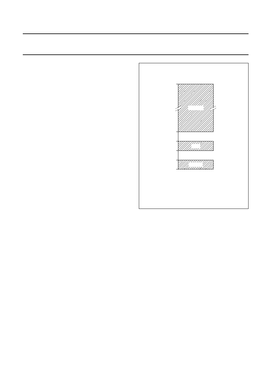
handbook, halfpage
MGR176
18
VMODE
(V)
4
3
2
1
0
Mute
Operating
Standby
Fig.3
Switching levels of the mode select pin
(pin MODE).

