 | –≠–ª–µ–∫—Ç—Ä–æ–Ω–Ω—ã–π –∫–æ–º–ø–æ–Ω–µ–Ω—Ç: TDA6101 | –°–∫–∞—á–∞—Ç—å:  PDF PDF  ZIP ZIP |

DATA SHEET
Preliminary specification
Supersedes data of November 1991
File under Integrated Circuits, IC02
1995 Feb 07
INTEGRATED CIRCUITS
Philips Semiconductors
TDA6101Q
Video output amplifier

1995 Feb 07
2
Philips Semiconductors
Preliminary specification
Video output amplifier
TDA6101Q
FEATURES
∑
High bandwidth and high slew rate
∑
No external heatsink required
∑
Black-current measurement output for Automatic
Black-current Stabilization (ABS)
∑
Two cathode outputs; one for DC currents, and one for
transient currents
∑
A feedback output separated from the cathode outputs
∑
Internal protection against positive appearing
Cathode-Ray Tube (CRT) flashover discharges
∑
ESD protection
∑
Simple application with a variety of colour decoders
∑
Differential input with a designed maximum common
mode input capacitance of 3 pF, a maximum differential
mode input capacitance of 0.5 pF and a differential input
voltage temperature drift of 20
µ
V/K
∑
Defined switch-off behaviour.
GENERAL DESCRIPTION
The TDA6101Q is a video output amplifier with 9 MHz
bandwidth. The device is contained in a single in-line 9-pin
medium power (DBS9MPF) package, using high-voltage
DMOS technology, intended to drive the cathode of a
colour CRT.
QUICK REFERENCE DATA
ORDERING INFORMATION
SYMBOL
PARAMETER
CONDITIONS
MIN.
TYP.
MAX.
UNIT
V
DDH
high level supply voltage
0
-
250
V
V
DDL
low level supply voltage
0
-
14
V
I
DDH
quiescent high voltage supply current
V
oc
= 0.5V
DDH
3.5
4.4
5.5
mA
I
DDL
quiescent low voltage supply current
V
oc
= 0.5V
DDH
2.2
2.8
3.5
mA
V
I
input voltage
0
-
V
DDL
V
V
oc
, V
fb
output voltage
V
DDL
-
V
DDH
V
T
stg
storage temperature
-
55
-
+150
∞
C
T
amb
operating ambient temperature
-
20
-
+65
∞
C
TYPE NUMBER
PACKAGE
NAME
DESCRIPTION
VERSION
TDA6101Q
DBS9MPF
plastic DIL-bent-SIL medium power package with fin; 9 leads
SOT111-1
1995 Feb 07
3
Philips Semiconductors
Preliminary specification
Video output amplifier
TDA6101Q
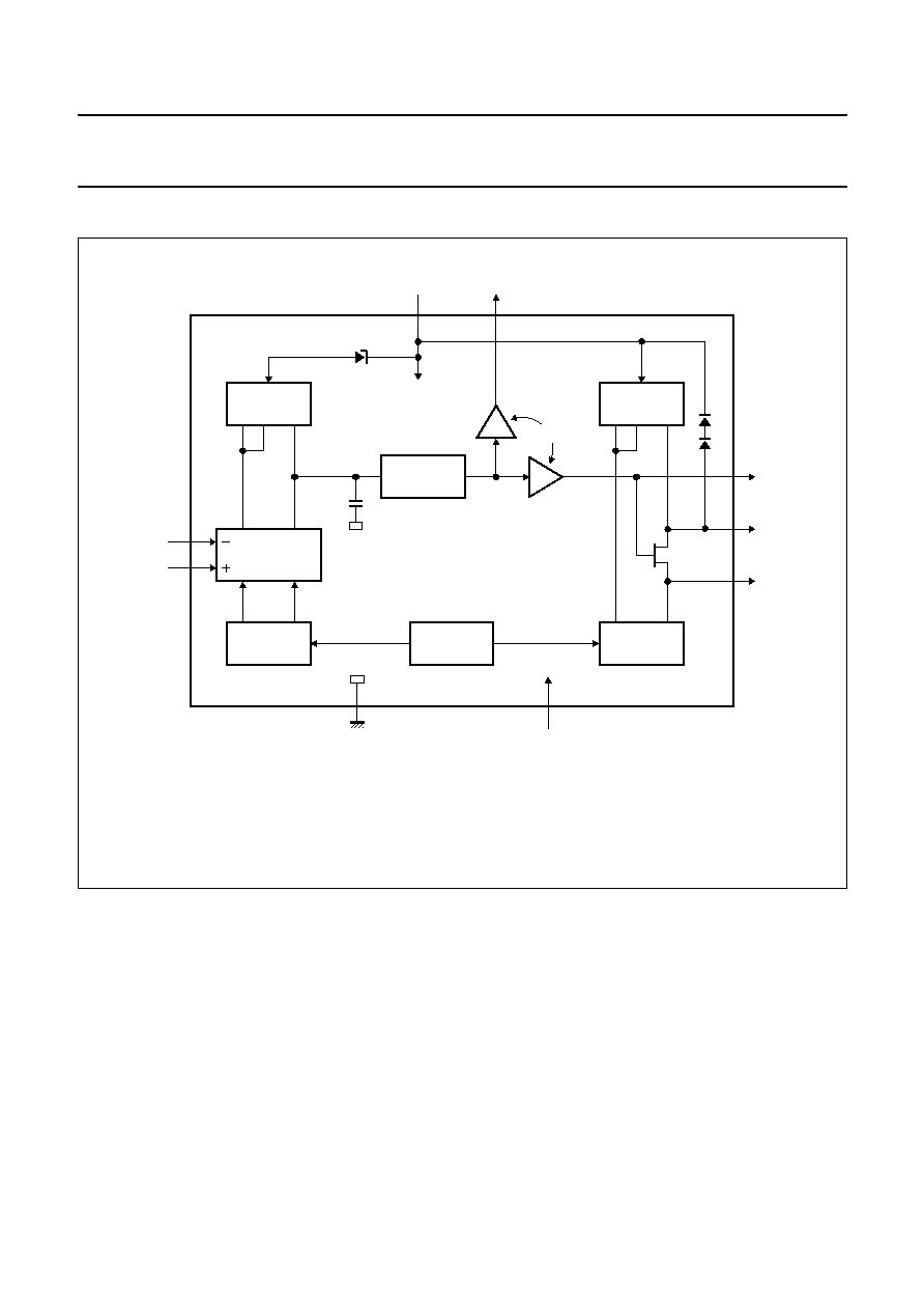
BLOCK DIAGRAM
Fig.1 Block diagram.
handbook, full pagewidth
DIFFERENTIAL
STAGE
MIRROR
MIRROR
CURRENT
SOURCE
MIRROR
MIRROR
TDA6101Q
7 V
supply voltage
input HIGH
feedback
output
6
Vbias
C par
9
non-inverting
input
inverting
input
3
1
4
2
ground
(substrate)
supply voltage
input LOW
7
8
5
cathode
transient
output
cathode
DC output
black current
measurement
output
MCD356
FOLLOWERS

1995 Feb 07
4
Philips Semiconductors
Preliminary specification
Video output amplifier
TDA6101Q
PINNING
SYMBOL
PIN
DESCRIPTION
V
ip
1
non-inverting voltage input
V
DDL
2
supply voltage LOW
V
in
3
inverting voltage input
GND
4
ground, substrate
I
om
5
black current measurement
output
V
DDH
6
supply voltage HIGH
V
cn
7
cathode transient voltage output
V
oc
8
cathode DC voltage output
V
fb
9
feedback voltage output
Fig.2 Pin configuration.
handbook, halfpage
MCD355
1
2
3
4
5
6
7
8
9
DDL
V
GND
TDA6101Q
ip
V
in
V
om
I
oc
V
cn
V
fb
V
DDH
V

1995 Feb 07
5
Philips Semiconductors
Preliminary specification
Video output amplifier
TDA6101Q
LIMITING VALUES
In accordance with the Absolute Maximum Rating System (IEC 134). Voltages measured with respect to GND (pin 4);
currents as specified in Fig.1; unless otherwise specified.
HANDLING
Inputs and outputs are protected against electrostatic discharge in normal handling. However, to be totally safe, it is
desirable to take normal precautions appropriate to handling MOS devices (see
"Handling MOS Devices" ).
QUALITY SPECIFICATION
Quality specification
"SNW-FQ-611 part E" is applicable, except for ESD Human body model see Chapter "Limiting
values", and can be found in the
"Quality reference handbook" (ordering number 9398 510 63011).
THERMAL CHARACTERISTICS
Note
1. External heatsink not required.
SYMBOL
PARAMETER
CONDITIONS
MIN.
MAX.
UNIT
V
DDH
high level supply voltage
0
250
V
V
DDL
low level supply voltage
0
14
V
V
I
input voltage
0
V
DDL
V
V
Idm
differential mode input voltage
-
6
+6
V
V
om
measurement output voltage
0
V
DDL
V
oc
cathode output voltage
V
DDL
V
DDH
V
V
fb
feedback output voltage
V
DDL
V
DDH
V
I
in
,I
ip
input current
0
1
mA
I
ocsmL
low non-repetitive peak cathode
output current
flashover discharge = 100
µ
C
0
5
A
I
ocsmH
high non-repetitive peak cathode
output current
flashover discharge = 100 nC
0
10
A
P
tot
total power dissipation
0
1.9
W
T
stg
storage temperature
-
55
+150
∞
C
T
j
junction temperature
-
20
+150
∞
C
V
es
electrostatic handling
human body model (HBM)
-
> 1500
V
machine model (MM)
-
> 400
V
SYMBOL
PARAMETER
(1)
VALUE
UNIT
R
th j-a
thermal resistance from junction to ambient in free air
56
K/W
R
th j-c
thermal resistance from junction to case
12
K/W