 | ÐлекÑÑоннÑй компоненÑ: TDA8341 | СкаÑаÑÑ:  PDF PDF  ZIP ZIP |
Äîêóìåíòàöèÿ è îïèñàíèÿ www.docs.chipfind.ru

DATA SHEET
Product specification
File under Integrated Circuits, IC02
November 1987
INTEGRATED CIRCUITS
TDA8340
TDA8341
Television IF amplifier and
demodulator
November 1987
2
Philips Semiconductors
Product specification
Television IF amplifier and demodulator
TDA8340
TDA8341
DESCRIPTION
The TDA8340;Q and TDA8341;Q are integrated IF
amplifier and demodulator circuits for colour or black/white
television receivers, the TDA8340;Q is for application with
n-p-n tuners and the TDA8341;Q for p-n-p tuners.
The TDA8340;Q and TDA8341;Q are pin-compatible
successors with improved performance to types
TDA2540/2541;Q and TDA3540/3541;Q.
Features
·
Full range gain-controlled wide-band IF amplifier
·
Linear synchronous demodulator with excellent
intermodulation performance
·
White spot inverter
·
Wide-band video amplifier with noise protection
·
AFC circuit with AFC on/off switching and
sample-and-hold function
·
Low impedance AFC output
·
AGC circuit with noise gating
·
Tuner AGC output for n-p-n tuners (TDA8340) or p-n-p
tuners (TDA8341)
·
External video switch for switching-off the video output
·
Reduced sensitivity for high sound carriers
·
Integrated filter to limit second harmonic IF signals
·
Wide supply voltage range
·
Requires few external components
QUICK REFERENCE DATA
PACKAGE OUTLINES
TDA8340; TDA8341:
16-lead DIL; plastic (SOT38); SOT38-1; 1996 november 29.
PARAMETER
CONDITIONS
SYMBOL
MIN.
TYP.
MAX.
UNIT
Supply voltage (pin 11)
V
CC
= V
11-13
9,4
12
13,2
V
Supply current (pin 11)
I
11
30
42
55
mA
IF input sensitivity
(r.m.s. value)
V
1-16(rms)
20
40
80
µ
V
IF gain control range
G
v
-
67
-
dB
Video output voltage
white signal;
(peak-to-peak value)
10% top sync
V
12
-
13(p
-
p)
2,4
2,7
3,0
V
Signal-to-noise ratio
V
i
= 10 mV
S/(S
+
N)
50
58
-
dB
AFC output voltage swing
(peak-to-peak value)
V
5-13(p-p)
-
10
-
V
November 1987
3
Philips Semiconductors
Product specification
Television IF amplifier and demodulator
TDA8340
TDA8341
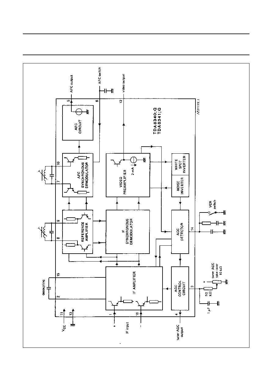
Fig.1 Block diagram.

November 1987
4
Philips Semiconductors
Product specification
Television IF amplifier and demodulator
TDA8340
TDA8341
PINNING
FUNCTIONAL DESCRIPTION
IF amplifier
This is a 3-stage, gain-controlled IF amplifier with a wide dynamic range. On-chip capacitors in the d.c. feedback loop of
the amplifier maintain stability at maximum gain. Internal stabilization of the supply voltage ensures the desired sensitivity
and gain control range over the whole supply voltage range and also gives very good power supply ripple rejection in this
part of the circuit.
Demodulator
The redesigned IF demodulator is a quasi-synchronous circuit that employs passive carrier regeneration and logarithmic
clamping to give improved signal handling. The demodulator input is a.c. coupled to the IF amplifier to reduce d.c. offsets
and thus minimize residual IF carrier in the output signal.
Video amplifier
The linearity and bandwidth of the video amplifier are sufficient to meet all wide band requirements, e.g. for teletext
transmissions. Second harmonics of the IF carrier are effectively reduced by a Sallen-Key low pass interstage filter
between the demodulator output and the video amplifier input. An integrated filter in the noise inverter reduces the
sensitivity of the video amplifier for high sound carriers.
White spot protection comprises a white spot clamp system combined with a delayed-action inverter which is also highly
resistant to high sound carriers.
Note. To prevent radiated video output at the input pins, connect a 6,8
µ
H inductor in series with pin 12 and fit as close
as possible to the IC body. Use short leads.
AGC detector
A Bessel low-pass filter between the video output and the AGC detector improves the detector function in the presence
of high sound carriers. No `hang-up' occurs in the detector after pin 14 has been short-circuited to ground (VCR switch
operated). The detector also generates the sample-and-hold pulse for the AFC system.
1 and 16
Balanced IF inputs
2 and 15
IF amplifier decoupling
3
Tuner AGC starting point adjustment
4
Tuner AGC output
5
AFC output
6
AFC on/off switch and sample-and-hold capacitor
7 and 10
Reference carrier
/2 rad. phase shift
8 and 9
IF picture carrier passive regeneration
11
Positive supply voltage (V
CC
)
12
Video output
13
Ground (V
EE
)
14
IF AGC capacitor and VCR switch

November 1987
5
Philips Semiconductors
Product specification
Television IF amplifier and demodulator
TDA8340
TDA8341
AGC control circuit
This converts the AGC detector voltage (pin 14) into a current signal which controls the gain of the IF amplifier. It also
provides a tuner AGC control output from pin 4, current limiting is incorporated to prevent internal damage. The AGC
starting point is adjusted via pin 3.
AFC circuit
The AFC circuit provides a voltage output which controls the IF frequency of the tuner. Video information on the AFC
output (pin 5) is eliminated by a sample-and-hold circuit (external capacitor at pin 6). Coupling between the AFC and
reference tuned circuits is via two small capacitors (or parasitic capacitance) between the respective tracks of the printed
circuit board. If the capacitance is less than 1 pF, the steepness of the AFC characteristic is reduced.
RATINGS
Limiting values in accordance with the Absolute Maximum System (IEC 134)
PARAMETER
SYMBOL
MIN.
MAX.
UNIT
Supply voltage (pin 11)
V
CC
= V
11
-
13
9,4
13,2
V
IF AGC voltage/VCR switch
V
14-13
-
13,2
V
Tuner AGC voltage
V
4-13
-
12
V
AFC switch voltage
V
6-13
-
13,2
V
Maximum voltage level with
VCR switch active
V
12-13
-
5,0
V
DC current at video output
I
12
-
10
mA
DC current at AFC output
I
5
-
10
mA
Total power dissipation
P
tot
-
1,2
W
Storage temperature range
T
stg
-
55
+
150
°
C
Operating ambient temperature
T
amb
-
25
+
70
°
C

November 1987
6
Philips Semiconductors
Product specification
Television IF amplifier and demodulator
TDA8340
TDA8341
CHARACTERISTICS
Measured in circuit of Fig.3; V
CC
= 12 V; T
amb
= 25
°
C; unless otherwise specified
PARAMETER
CONDITIONS
SYMBOL
MIN.
TYP.
MAX.
UNIT
Supply voltage (pin 11)
V
CC
= V
11
-
13
9,4
12
13,2
V
Supply current
no input signal
I
11
30
42
55
mA
IF amplifier (note 1)
Input sensitivity
at onset of AGC
V
1
-
16
20
40
80
µ
V
Differential input resistance
R
1
-
16
-
2
-
k
Differential input
capacitance
C
1
-
16
-
3
-
pF
Gain control range
G
v
-
67
-
dB
Input signal variation
note 2
V
12
-
13
-
-
0,5
dB
Maximum input signal
V
1
-
16
100
-
-
mV
Tuner AGC (note 1)
Tuner AGC starting point
R
3
-
11
= 39 k
V
1
-
16
-
-
3
mV
(note 3)
R
3
-
13
= 39 k
V
1-16
70
-
-
mV
Maximum current swing
of tuner AGC output
I
4
10
-
-
mA
Input signal variation
note 4;
I
4
= 1 to 9 mA
V
1-16
-
-
3
dB
Output saturation voltage
I
4
= 7 mA
V
4-13
-
200
300
mV
Leakage current
V
4
= 12 V
I
4
-
-
1
µ
A
Video output (note 4)
Zero-signal output level
note 5
V
12-13
5,7
6,0
6,3
V
Top sync output level
V
12-13
2,8
3,0
3,2
V
Video output voltage
white signal;
(peak-to-peak value)
10% top sync
V
12-13(p-p)
2,4
2,7
3,0
V
Internal bias current
of emitter follower
output transistor
1,4
2,2
3,0
mA
Output impedance
Z
12
-
100
-
Bandwidth of demodulated
output signal
B
6
7,5
-
MHz
Differential gain
note 6
G
d
-
2
5
%
Differential phase
note 6
d
-
2
5
deg
Luminance non-linearity
note 7
-
2
5
%
Residual carrier signal
(r.m.s. value)
note 8
V
12
-
13(rms)
-
2
10
mV

November 1987
7
Philips Semiconductors
Product specification
Television IF amplifier and demodulator
TDA8340
TDA8341
Residual 2nd harmonic
of carrier signal
(r.m.s. value)
note 8
V
12-13(rms)
-
2
10
mV
Variation of video voltage for
V
CC
= 1 V
0,1
0,2
0,3
Intermodulation
notes 8 and 9;
1,1 MHz, blue
-
-
65
-
60
dB
1,1 MHz, yellow
-
-
60
-
56
dB
3,3 MHz
-
-
-
68
dB
Signal-to-noise ratio
note 10;
V
i
= 10 mV
S/(S
+
N)
50
58
-
dB
max. gain
S/(S
+
N)
54
61
-
dB
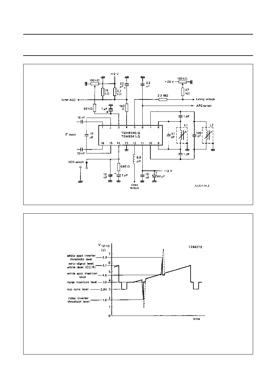
Spot inverter (note 11)
Threshold level
V
12-13
6,3
6,8
7,3
V
Insertion level
V
12-13
4,2
4,5
4,8
V
Noise inverter (note 11)
Threshold level
V
12-13
1,6
1,8
2,0
V
Insertion level
V
12-13
3,5
3,8
4,1
V
VCR switch
Level below which video
output switches off
V
14-13
1,8
2,2
2,6
V
Switch current
V
12
-
13
= 0,7 V
-
I
14
40
60
100
µ
A
AFC circuit (note 12)
Output voltage swing
(peak-to-peak value)
V
5-13(p-p)
-
10
-
V
Change of frequency for
an AFC output voltage
swing of 10 V
f
-
60
120
kHz
AFC output voltage
at f = 38,9 MHz
V
5-13
-
6
-
V
no input signal
V
5-13
2
6
10
V
during AFC off
V
5-13
5
6
7
V
AFC output resistance
R
5-13
-
500
-
AFC switch:
level below which AFC
output switches off
V
6-13
1,4
2,0
2,8
V
AFC switch current
during AFC on
I
6
-
200
500
µ
A
Max. AFC switch current
during AFC off;
V
6
-
13
= 0 V
I
6
-
-
5
mA
PARAMETER
CONDITIONS
SYMBOL
MIN.
TYP.
MAX.
UNIT
V
12
13 p
p
(
)
V
11 13
-------------------------------------
November 1987
8
Philips Semiconductors
Product specification
Television IF amplifier and demodulator
TDA8340
TDA8341
Notes
1. All input signals are measured r.m.s. at top sync and 38,9 MHz.
2. Measured with 0 dB = 200
µ
V.
3. Tuner AGC starting point is defined as `level of input signal when tuner AGC current = 1 mA'.
4. Measured with pin 3 connected via 39 k
resistor to V
CC
(pin 11), with an r.m.s. voltage of 10 mV top sync input
signal and with pin 12 not loaded.
5. At the `projected zero point', e.g. with switched demodulator.
6. Measured in the circuit of Fig.7:
the differential gain is expressed as a percentage of the difference in peak amplitudes between the largest and
smallest value relative to the subcarrier amplitude at blanking level;
the differential phase is defined as `the difference (in degrees) between the largest and smallest phase angles'.
7. Measured according to the test line shown in Fig.9:
the non-linearity is expressed as a percentage of the maximum deviation of a luminance step from the mean step,
with respect to the mean step;
the mean step is (white level
-
black level) divided by the number of steps.
8. Measured up to 45 dB gain control.
9. Test set-up and input conditions for intermodulation measurements as in Figs 6 and 7.
10. Measured with a 75
source:
11. Video output waveform showing white spot and noise inverter threshold levels.
12. Measured with input signal V
1-16
= 10 mV and with no load at AFC output.
S
S
N
+
(
)
/
20log
V
out black to white
V
n rms
(
)
at B
5 MHz
=
--------------------------------------------------------
=
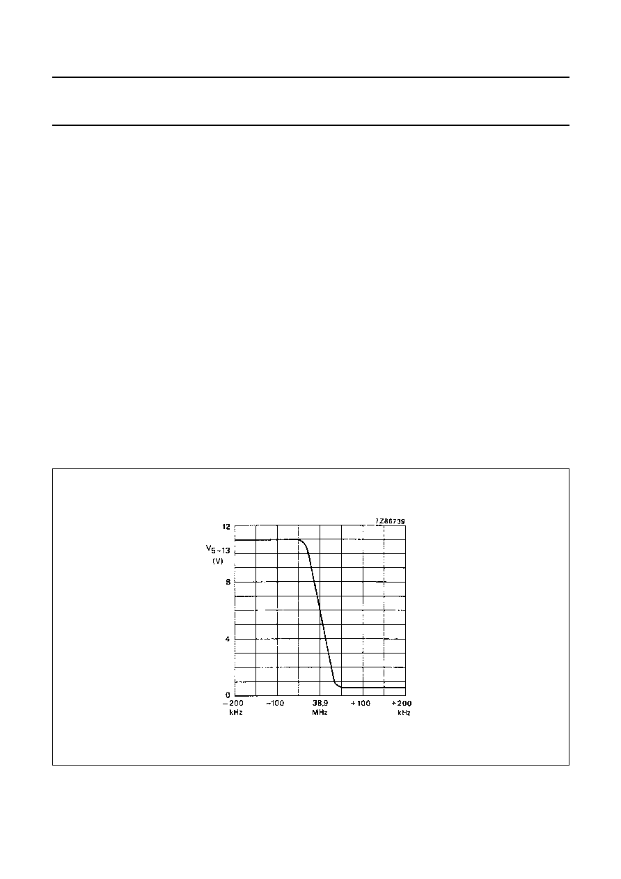
Fig.2 AFC output voltage as a function of frequency.
November 1987
9
Philips Semiconductors
Product specification
Television IF amplifier and demodulator
TDA8340
TDA8341
Fig.3 Typical application circuit diagram; Q of L1 and L2 = 80; f
o
= 38,9 MHz.
Fig.4 Video output waveform showing white spot and noise inverter threshold levels.
November 1987
10
Philips Semiconductors
Product specification
Television IF amplifier and demodulator
TDA8340
TDA8341
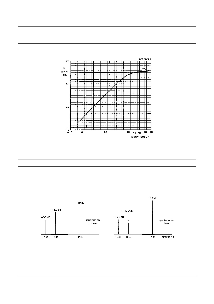
Fig.5 Signal-to-noise ratio as a function of input voltage.
Fig.6 Input conditions for intermodulation measurements; standard colour bar with 75% contrast.
S.C.: sound carrier level
; with respect to top sync level
C.C.: chrominance carrier level ; with respect to top sync level
P.C.: picture carrier level
; with respect to top sync level
November 1987
11
Philips Semiconductors
Product specification
Television IF amplifier and demodulator
TDA8340
TDA8341
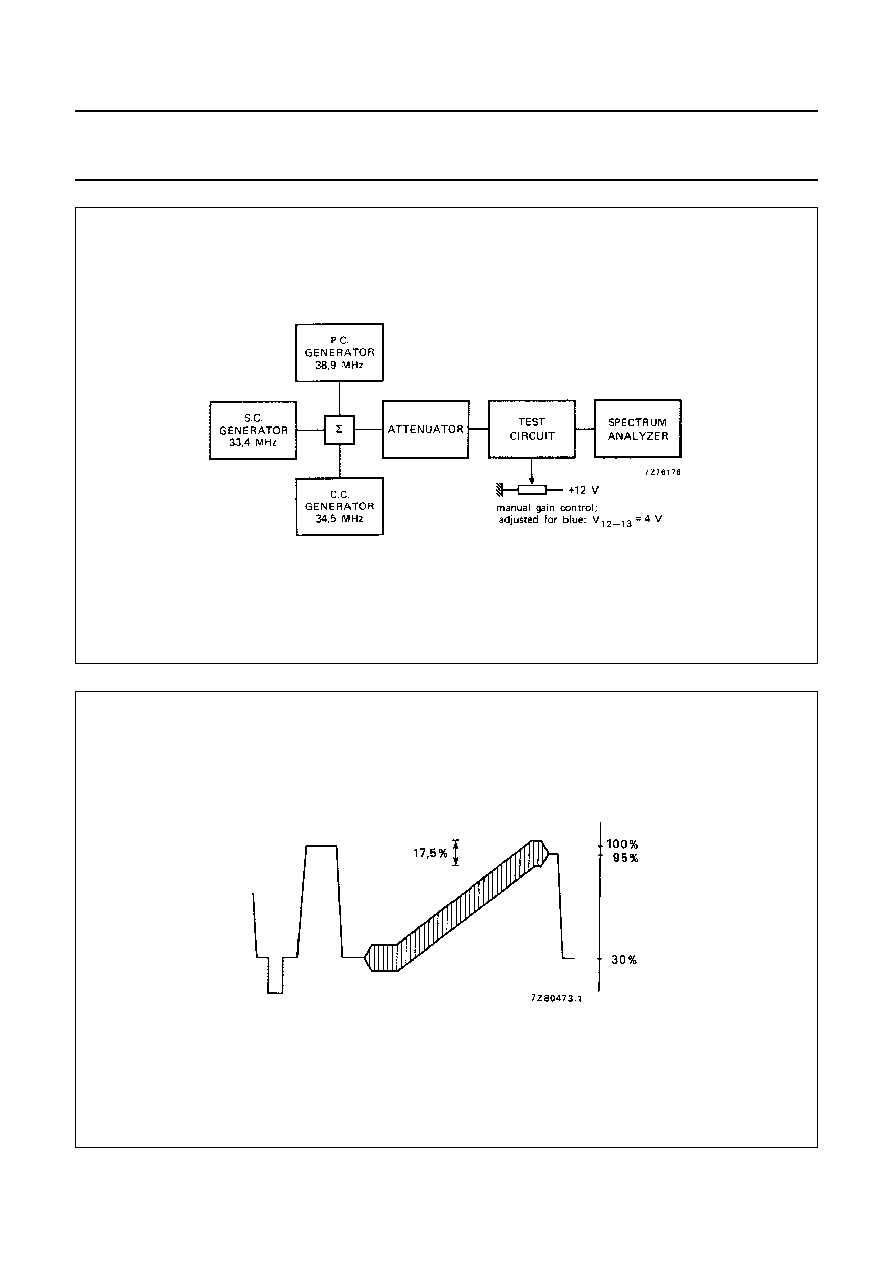
Fig.7 Test set-up for intermodulation measurements.
Fig.8 Video output signal.
November 1987
12
Philips Semiconductors
Product specification
Television IF amplifier and demodulator
TDA8340
TDA8341
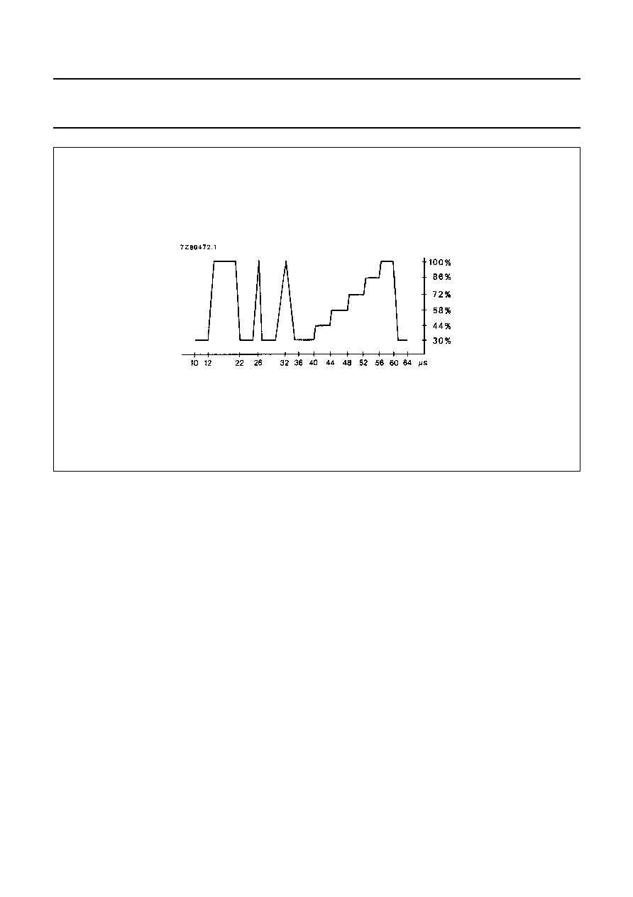
Fig.9 E.B.U. test signal waveform (line 330).
November 1987
13
Philips Semiconductors
Product specification
Television IF amplifier and demodulator
TDA8340
TDA8341
PACKAGE OUTLINE
UNIT
A
max.
1
2
b
1
c
E
e
M
H
L
REFERENCES
OUTLINE
VERSION
EUROPEAN
PROJECTION
ISSUE DATE
IEC
JEDEC
EIAJ
mm
inches
DIMENSIONS (inch dimensions are derived from the original mm dimensions)
SOT38-1
92-10-02
95-01-19
A
min.
A
max.
b
max.
w
M
E
e
1
1.40
1.14
0.055
0.045
0.53
0.38
0.32
0.23
21.8
21.4
0.86
0.84
6.48
6.20
0.26
0.24
3.9
3.4
0.15
0.13
0.254
2.54
7.62
0.30
8.25
7.80
0.32
0.31
9.5
8.3
0.37
0.33
2.2
0.087
4.7
0.51
3.7
0.15
0.021
0.015
0.013
0.009
0.01
0.10
0.020
0.19
050G09
MO-001AE
M
H
c
(e )
1
M
E
A
L
seating plane
A
1
w
M
b
1
e
D
A
2
Z
16
1
9
8
b
E
pin 1 index
0
5
10 mm
scale
Note
1. Plastic or metal protrusions of 0.25 mm maximum per side are not included.
(1)
(1)
D
(1)
Z
DIP16: plastic dual in-line package; 16 leads (300 mil); long body
SOT38-1
November 1987
14
Philips Semiconductors
Product specification
Television IF amplifier and demodulator
TDA8340
TDA8341
SOLDERING
Introduction
There is no soldering method that is ideal for all IC packages. Wave soldering is often preferred when through-hole and
surface mounted components are mixed on one printed-circuit board. However, wave soldering is not always suitable for
surface mounted ICs, or for printed-circuits with high population densities. In these situations reflow soldering is often
used.
This text gives a very brief insight to a complex technology. A more in-depth account of soldering ICs can be found in our
"IC Package Databook" (order code 9398 652 90011).
Soldering by dipping or by wave
The maximum permissible temperature of the solder is 260
°
C; solder at this temperature must not be in contact with the
joint for more than 5 seconds. The total contact time of successive solder waves must not exceed 5 seconds.
The device may be mounted up to the seating plane, but the temperature of the plastic body must not exceed the
specified maximum storage temperature (T
stg max
). If the printed-circuit board has been pre-heated, forced cooling may
be necessary immediately after soldering to keep the temperature within the permissible limit.
Repairing soldered joints
Apply a low voltage soldering iron (less than 24 V) to the lead(s) of the package, below the seating plane or not more
than 2 mm above it. If the temperature of the soldering iron bit is less than 300
°
C it may remain in contact for up to
10 seconds. If the bit temperature is between 300 and 400
°
C, contact may be up to 5 seconds.
DEFINITIONS
LIFE SUPPORT APPLICATIONS
These products are not designed for use in life support appliances, devices, or systems where malfunction of these
products can reasonably be expected to result in personal injury. Philips customers using or selling these products for
use in such applications do so at their own risk and agree to fully indemnify Philips for any damages resulting from such
improper use or sale.
Data sheet status
Objective specification
This data sheet contains target or goal specifications for product development.
Preliminary specification
This data sheet contains preliminary data; supplementary data may be published later.
Product specification
This data sheet contains final product specifications.
Limiting values
Limiting values given are in accordance with the Absolute Maximum Rating System (IEC 134). Stress above one or
more of the limiting values may cause permanent damage to the device. These are stress ratings only and operation
of the device at these or at any other conditions above those given in the Characteristics sections of the specification
is not implied. Exposure to limiting values for extended periods may affect device reliability.
Application information
Where application information is given, it is advisory and does not form part of the specification.
Document Outline
- DESCRIPTION
- QUICK REFERENCE DATA
- PACKAGE OUTLINES
- PINNING
- FUNCTIONAL DESCRIPTION
- IF amplifier
- Demodulator
- Video amplifier
- AGC detector
- AGC control circuit
- AFC circuit
- RATINGS
- CHARACTERISTICS
- PACKAGE OUTLINE
- SOLDERING
- DEFINITIONS
- LIFE SUPPORT APPLICATIONS