2004 Feb 24
2
Philips Semiconductors
Product specification
I
2
C-bus controlled 4
�
50 Watt power
amplifier and multiple voltage regulator
TDA8588J; TDA8588xJ
FEATURES
Amplifiers
�
I
2
C-bus control
�
Can drive a 2
load with a battery voltage of up to 16 V
and a 4
load with a battery voltage of up to 18 V
�
DC load detection, open, short and present
�
AC load (tweeter) detection
�
Programmable clip detect; 1 % or 4 %
�
Programmable thermal protection pre-warning
�
Independent short-circuit protection per channel
�
Low gain line driver mode (20 dB)
�
Loss-of-ground and open V
P
safe
�
All outputs protected from short-circuit to ground, to V
P
or across the load
�
All pins protected from short-circuit to ground
�
Soft thermal-clipping to prevent audio holes
�
Low battery detection.
Voltage regulators
G
ENERAL
�
I
2
C-bus control
�
Good stability for any regulator with almost any output
capacitor value
�
Five voltage regulators (microcontroller, display,
mechanical digital, mechanical drive and audio)
�
Choice of non-adjustable 3.3 or 5 V microcontroller
supply (REG2) versions reducing risk of overvoltage
damage
�
Choice of non-adjustable 3.3 or 5 V digital signal
processor supply (REG3) versions reducing risk of
overvoltage damage
�
Selectable output voltages for regulators 1, 4 and 5
�
Low dropout voltage PNP output stages
�
High supply voltage ripple rejection
�
Low noise for all regulators
�
Two power switches (antenna switch and amplifier
switch)
�
Regulator 2 (microcontroller supply) operational during
load-dump and thermal shut-down
�
Low quiescent current (only regulator 2 is operational)
�
Reset output (push-pull output stage)
�
Adjustable reset delay time
�
Backup functionality.
P
ROTECTION
�
If connection to the battery voltage is reversed, all
regulator voltages will be zero
�
Able to withstand voltages at the output of up to 18 V
(supply line may be short-circuited)
�
Thermal protection to avoid thermal breakdown
�
Load-dump protection
�
Regulator outputs protected from DC short-circuit to
ground or to supply voltage
�
All regulators protected by foldback current limiting
�
Power switches protected from loss-of-ground.
APPLICATIONS
�
Boost amplifier and voltage regulator for car radios and
CD/MD players.
GENERAL DESCRIPTION
Amplifiers
The TDA8588 has a complementary quad audio power
amplifier that uses BCDMOS technology. It contains four
amplifiers configured in Bridge Tied Load (BTL) to drive
speakers for front and rear left and right channels. The
I
2
C-bus allows diagnostic information of each amplifier and
its speaker to be read separately. Both front and both rear
channel amplifiers can be configured independently in line
driver mode with a gain of 20 dB (differential output).
Voltage regulators
The TDA8588 has a multiple output voltage regulator with
two power switches.
The voltage regulator contains the following:
�
Four switchable regulators and one permanently active
regulator (microcontroller supply)
�
Two power switches with loss-of-ground protection
�
A reset output that can be used to communicate with a
microcontroller.
The quiescent current has a very low level of 150
�
A with
only regulator 2 active.

2004 Feb 24
3
Philips Semiconductors
Product specification
I
2
C-bus controlled 4
�
50 Watt power
amplifier and multiple voltage regulator
TDA8588J; TDA8588xJ
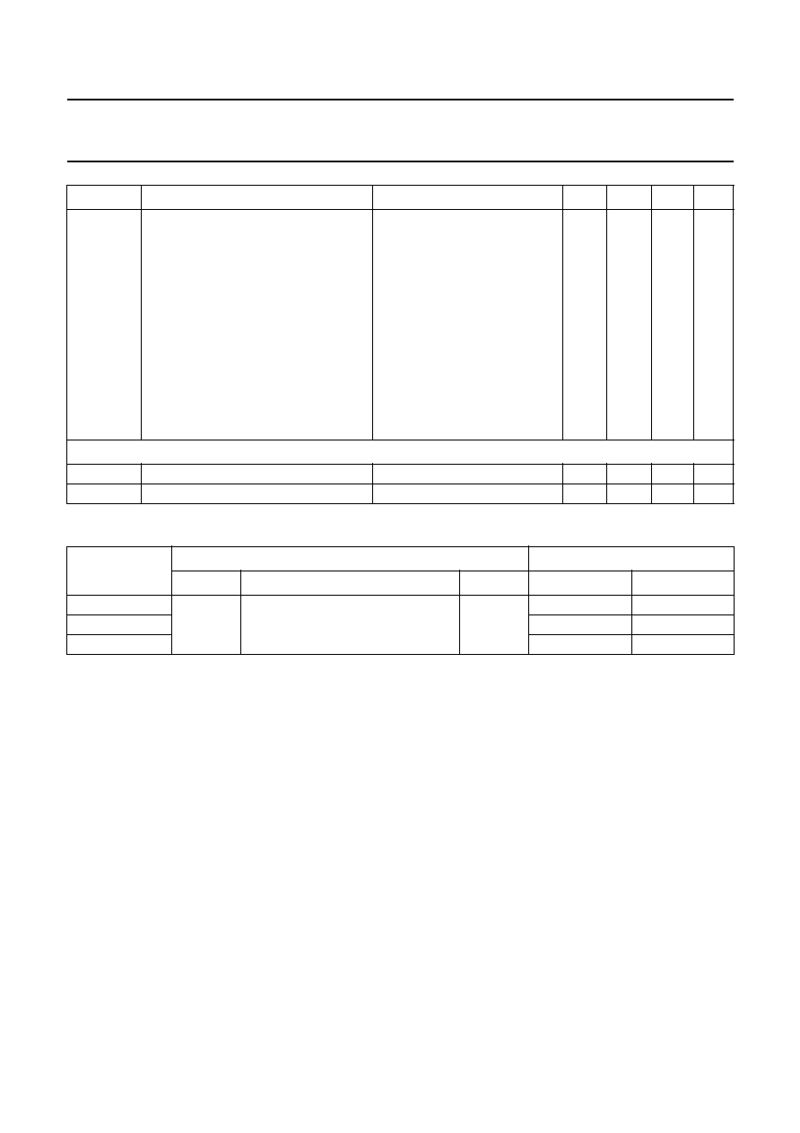
QUICK REFERENCE DATA
SYMBOL
PARAMETER
CONDITIONS
MIN.
TYP.
MAX. UNIT
Amplifiers
V
P1
, V
P2
operating supply voltage
8
14.4
18
V
I
q(tot)
total quiescent current
-
270
400
mA
P
o(max)
maximum output power
R
L
= 4
; V
P
= 14.4 V; V
IN
= 2 V
RMS square wave
44
46
-
W
R
L
= 4
; V
P
= 15.2 V; V
IN
= 2 V
RMS square wave
49
52
-
W
R
L
= 2
; V
P
= 14.4 V; V
IN
= 2 V
RMS square wave
83
87
-
W
THD
total harmonic distortion
-
0.01
0.1
%
V
n(o)(amp)
noise output voltage in amplifier mode
-
50
70
�
V
V
n(o)(LN)
noise output voltage in line driver mode
-
25
35
�
V
Voltage regulators
S
UPPLY
V
P
supply voltage
regulator 1, 3, 4 and 5 on
10
14.4
18
V
regulator 2 on
4
-
-
V
jump starts for t
10 minutes
-
-
30
V
load dump protection for
t
50 ms and t
r
2.5 ms
-
-
50
V
overvoltage for shut-down
20
-
-
V
I
q(tot)
total quiescent supply current
standby mode; V
P
= 14.4 V
-
150
190
�
A
V
OLTAGE REGULATORS
V
O(REG1)
output voltage of regulator 1
0.5 mA
I
O
400 mA;
selectable via I
2
C-bus
IB2[D3:D2] = 01
-
8.3
-
V
IB2[D3:D2] = 10
-
8.5
-
V
IB2[D3:D2] = 11
-
8.7
-
V
V
O(REG2)
output voltage of regulator 2
0.5 mA
I
O
350 mA
TDA8588J; TDA8588AJ
-
5.0
-
V
TDA8588BJ
-
3.3
-
V
V
O(REG3)
output voltage of regulator 3
0.5 mA
I
O
300 mA
TDA8588J
-
5.0
-
V
TDA8588AJ; TDA8588BJ
-
3.3
-
V
V
O(REG4)
output voltage of regulator 4
maximum current
1.6 A;
0.5 mA
I
O
800 mA;
selectable via I
2
C-bus
IB2[D7:D5] = 001
-
5.0
-
V
IB2[D7:D5] = 010
-
6.0
-
V
IB2[D7:D5] = 011
-
7.0
-
V
IB2[D7:D5] = 100
-
8.6
-
V