BUK7L11-34ARC
TrenchPLUS standard level FET
Rev. 03 -- 3 December 2003
Product data
1.
Product profile
1.1 Description
N-channel enhancement mode field-effect power transistor in a plastic package using
TrenchMOSTM technology, featuring very low on-state resistance, integral gate
resistor, ESD protection diodes and clamping diodes to protect the MOSFET from
avalanching.
1.2 Features
1.3 Applications
1.4 Quick reference data
2.
Pinning information
s
ESD and overvoltage protection
s
Q101 compliant
s
Internal gate resistor
s
On-state resistance 8 m
(typ).
s
12 V loads
s
Motors, lamps and solenoids.
s
V
DSR(CL)
= 41 V (typ)
s
R
DSon
= 8 m
(typ)
s
I
D
89 A
s
P
tot
172 W.
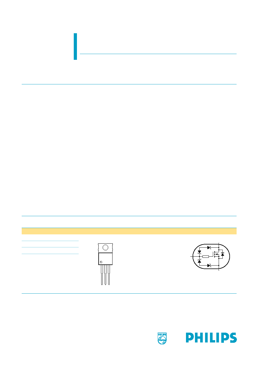
Table 1:
Pinning - SOT78C, simplified outline and symbol
Pin
Description
Simplified outline
Symbol
1
gate (g)
SOT78C (TO-220)
2
drain (d)
3
source (s)
mb
mounting base,
connected to drain (d)
1 2
mb
MBL370
3
d
s
g
MBL521

Philips Semiconductors
BUK7L11-34ARC
TrenchPLUS standard level FET
Product data
Rev. 03 -- 3 December 2003
2 of 14
9397 750 12163
� Koninklijke Philips Electronics N.V. 2003. All rights reserved.
3.
Ordering information
4.
Limiting values
[1]
Voltage is limited by clamping.
[2]
Current is limited by power dissipation chip rating.
[3]
Continuous current is limited by package.
Table 2:
Ordering information
Type number
Package
Name
Description
Version
BUK7L11-34ARC
TO-220
Plastic single-ended package; heatsink mounted; 1 mounting hole; 3 leads. SOT78C
Table 3:
Limiting values
In accordance with the Absolute Maximum Rating System (IEC 60134).
Symbol
Parameter
Conditions
Min
Max
Unit
V
DS
drain-source voltage (DC)
[1]
-
34
V
V
DGR
drain-gate voltage (DC)
R
GS
= 20 k
[1]
-
34
V
V
GS
gate-source voltage (DC)
[1]
-
�
20
V
I
D
drain current (DC)
T
mb
= 25
�
C; V
GS
= 10 V;
Figure 2
and
3
[2]
-
89
A
[3]
-
75
A
T
mb
= 100
�
C; V
GS
= 10 V;
Figure 2
[2]
-
63
A
I
DM
peak drain current
T
mb
= 25
�
C; pulsed; t
p
10
�
s;
Figure 3
-
358
A
P
tot
total power dissipation
T
mb
= 25
�
C;
Figure 1
-
172
W
I
DG(CL)
drain-gate clamping current
t
p
= 5 ms;
= 0.01
-
50
mA
I
GS(CL)
gate-source clamping current
continuous
-
10
mA
t
p
= 5 ms;
= 0.01
-
50
mA
T
stg
storage temperature
-
55
+175
�
C
T
j
junction temperature
-
55
+175
�
C
Source-drain diode
I
DR
reverse drain current (DC)
T
mb
= 25
�
C
[2]
-
89
A
[3]
-
75
A
I
DRM
peak reverse drain current
T
mb
= 25
�
C; pulsed; t
p
10
�
s
-
358
A
Avalanche ruggedness
E
DS(CL)S
non-repetitive drain-source clamped
energy
clamped inductive load; I
D
= 60 A;
V
DS
34 V; V
GS
= 10 V;
starting T
j
= 25
�
C
-
465
mJ
Electrostatic discharge
V
esd
electrostatic discharge voltage; all
pins
human body model; C = 100 pF;
R = 1.5 k
-
8
kV
human body model; C = 250 pF;
R = 1.5 k
-
6
kV
Philips Semiconductors
BUK7L11-34ARC
TrenchPLUS standard level FET
Product data
Rev. 03 -- 3 December 2003
3 of 14
9397 750 12163
� Koninklijke Philips Electronics N.V. 2003. All rights reserved.
V
GS
10 V
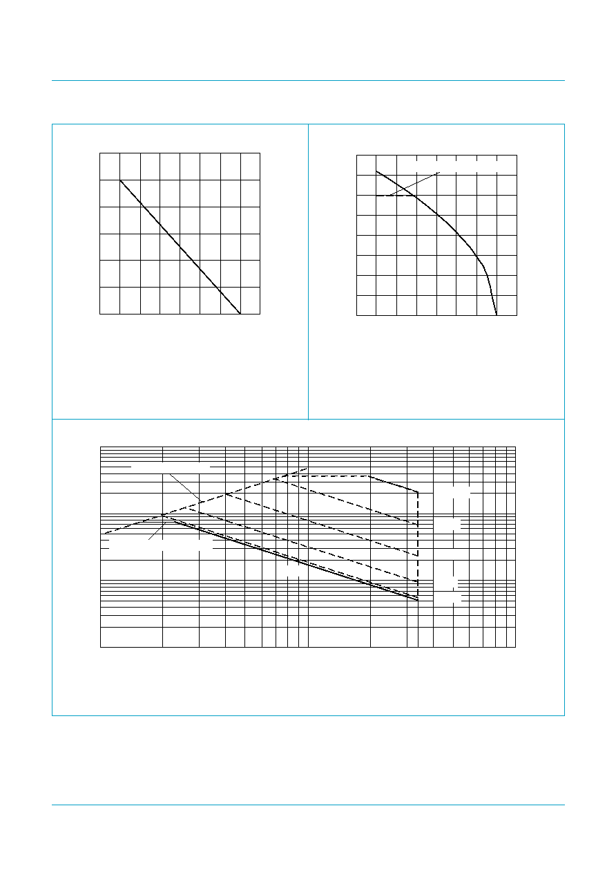
Fig 1.
Normalized total power dissipation as a
function of mounting base temperature.
Fig 2.
Continuous drain current as a function of
mounting base temperature.
T
mb
= 25
�
C; I
DM
single pulse.
Fig 3.
Safe operating area; continuous and peak drain currents as a function of drain-source voltage.
03na19
0
40
80
120
0
50
100
150
200
Tmb (
�
C)
Pder
(%)
03nj52
0
25
50
75
100
0
50
100
150
200
Tmb (
�
C)
ID
(A)
Capped at 75 A due to package
P
der
P
tot
P
tot 25 C
�
(
)
-----------------------
100%
�
=
03nj50
1
10
102
103
1
10
102
VDS (V)
ID
(A)
DC
100 ms
10 ms
Limit RDSon = VDS / ID
1 ms
tp = 10
�
s
100
�
s
Capped at 75 A due to package
Philips Semiconductors
BUK7L11-34ARC
TrenchPLUS standard level FET
Product data
Rev. 03 -- 3 December 2003
4 of 14
9397 750 12163
� Koninklijke Philips Electronics N.V. 2003. All rights reserved.
5.
Thermal characteristics
5.1 Transient thermal impedance
Table 4:
Thermal characteristics
Symbol
Parameter
Conditions
Min
Typ
Max
Unit
R
th(j-a)
thermal resistance from junction to
ambient
vertical in still air
-
60
-
K/W
R
th(j-mb)
thermal resistance from junction to
mounting base
Figure 4
-
0.55
0.87
K/W
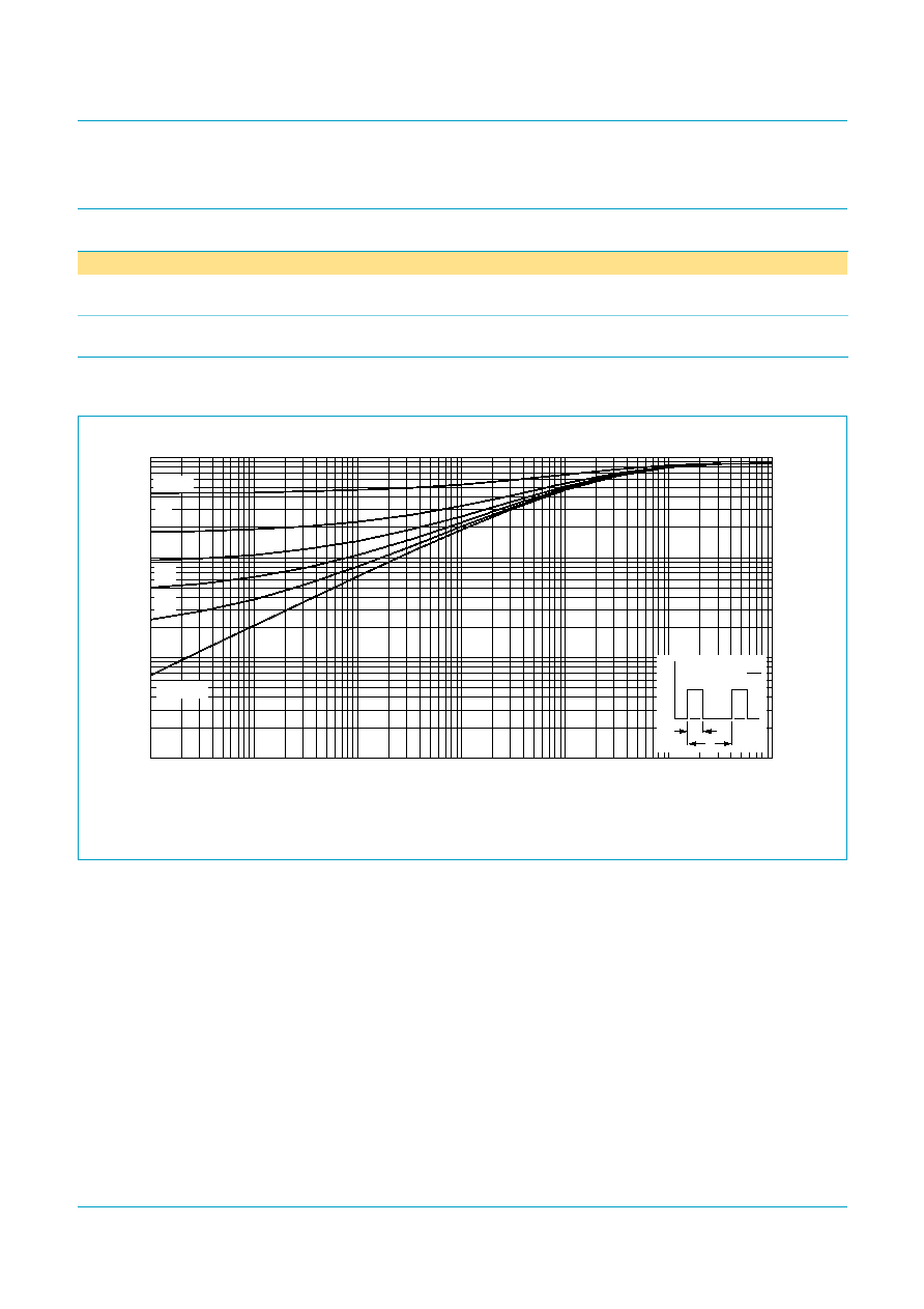
Fig 4.
Transient thermal impedance from junction to mounting base as a function of pulse duration.
03nj51
single shot
0.2
0.1
0.05
0.02
10-3
10-2
10-1
1
10-6
10-5
10-4
10-3
10-2
10-1
1
tp (s)
Zth(j-mb)
(K/W)
= 0.5
tp
tp
T
P
t
T
=

Philips Semiconductors
BUK7L11-34ARC
TrenchPLUS standard level FET
Product data
Rev. 03 -- 3 December 2003
5 of 14
9397 750 12163
� Koninklijke Philips Electronics N.V. 2003. All rights reserved.
6.
Characteristics
Table 5:
Characteristics
T
j
= 25
�
C unless otherwise specified.
Symbol
Parameter
Conditions
Min
Typ
Max
Unit
Static characteristics
V
(BR)DG
drain-gate zener breakdown
voltage
I
D
= 2 mA; V
GS
= 0 V
T
j
= 25
�
C
34
-
45
V
T
j
=
-
55
�
C
34
-
45
V
V
DSR(CL)
drain-source clamping
voltage (DC)
I
GS(CL)
=
-
2 mA; I
D
= 1 A
Figure 16
and
17
[1]
-
41
-
V
V
GS(th)
gate-source threshold voltage I
D
= 1 mA; V
DS
= V
GS
;
Figure 9
T
j
= 25
�
C
2.2
3
3.8
V
T
j
= 175
�
C
1.2
-
-
V
T
j
= 150
�
C
1.5
-
-
V
T
j
=
-
55
�
C
-
-
4.2
V
I
DSS
drain-source leakage current
V
DS
= 16 V; V
GS
= 0 V
T
j
= 25
�
C
-
0.1
2
�
A
T
j
= 150
�
C
-
3
50
�
A
T
j
= 175
�
C
-
18
250
�
A
V
(BR)GSS
gate-source breakdown
voltage
I
G
=
�
1 mA;
-
55
�
C < T
j
< +175
�
C
20
22
-
V
I
GSS
gate-source leakage current
V
GS
=
�
10 V; V
DS
= 0 V
T
j
= 25
�
C
-
5
1000
nA
T
j
= 175
�
C
-
-
50
�
A
V
GS
= 16 V; V
DS
= 0 V
T
j
= 175
�
C
-
-
150
�
A
R
DSon
drain-source on-state
resistance
V
GS
= 10 V; I
D
= 30 A;
Figure 7
and
8
T
j
= 25
�
C
-
8
11
m
T
j
= 175
�
C
-
-
20.9
m
V
GS
= 16 V; I
D
= 30 A
7
9.7
m
R
G
Internal gate resistor
-
11
-
Dynamic characteristics
Q
g(tot)
total gate charge
V
GS
= 10 V; V
DS
= 27 V;
I
D
= 25 A;
Figure 14
-
53
-
nC
Q
gs
gate-source charge
-
11
-
nC
Q
gd
gate-drain (Miller) charge
-
20
-
nC
C
iss
input capacitance
V
GS
= 0 V; V
DS
= 25 V;
f = 1 MHz;
Figure 12
-
1880
2506
pF
C
oss
output capacitance
-
640
768
pF
C
rss
reverse transfer capacitance
-
400
548
pF

Philips Semiconductors
BUK7L11-34ARC
TrenchPLUS standard level FET
Product data
Rev. 03 -- 3 December 2003
6 of 14
9397 750 12163
� Koninklijke Philips Electronics N.V. 2003. All rights reserved.
[1]
Independent testing of MOSFET and clamping diodes safeguards against avalanching.
t
d(on)
turn-on delay time
V
DS
= 30 V; R
L
= 1.2
;
V
GS
= 10 V; R
G
= 10
-
20
-
nS
t
r
rise time
-
92
-
nS
t
d(off)
turn-off delay time
-
127
-
nS
t
f
fall time
-
118
-
nS
L
d
internal drain inductance
measured from drain lead
6 mm from package to
center of die
-
4.5
-
nH
measured from contact
screw on mounting base to
center of die SOT78C
-
3.5
-
nH
L
s
internal source inductance
measured from source lead
to source bond pad
-
7.5
-
nH
Source-drain diode
V
SD
source-drain (diode forward)
voltage
I
S
= 10 A; V
GS
= 0 V;
Figure 15
-
0.85
1.2
V
t
rr
reverse recovery time
I
S
= 20 A; dI
S
/dt =
-
100 A/
�
s
V
GS
=
-
10 V; V
DS
= 30 V
-
52
-
ns
Q
r
recovered charge
-
28
-
nC
Table 5:
Characteristics
...continued
T
j
= 25
�
C unless otherwise specified.
Symbol
Parameter
Conditions
Min
Typ
Max
Unit

Philips Semiconductors
BUK7L11-34ARC
TrenchPLUS standard level FET
Product data
Rev. 03 -- 3 December 2003
7 of 14
9397 750 12163
� Koninklijke Philips Electronics N.V. 2003. All rights reserved.
T
j
= 25
�
C; t
p
= 300
�
s
T
j
= 25
�
C; I
D
= 30 A
Fig 5.
Output characteristics: drain current as a
function of drain-source voltage; typical values.
Fig 6.
Drain-source on-state resistance as a function
of gate-source voltage; typical values.
T
j
= 25
�
C; t
p
= 300
�
s
Fig 7.
Drain-source on-state resistance as a function
of drain current; typical values.
Fig 8.
Normalized drain-source on-state resistance
factor as a function of junction temperature.
03nj47
0
100
200
300
400
0
2
4
6
8
10
VDS (V)
ID
(A)
Label is VGS (V)
10
9.5
9
8.5
8
7.5
7
6.5
6
5.5
5
4.5
4
20
16
12
14
03nj46
5
10
15
20
25
30
5
10
15
20
VGS (V)
RDSon
(m
)
03nj48
5
10
15
20
25
0
100
200
300
400
ID (A)
RDSon
(m
)
5
6
7
8
10
20
Label is VGS (V)
03aa27
0
0.5
1
1.5
2
-60
0
60
120
180
Tj (
�
C)
a
a
R
DSon
R
DSon 25 C
�
(
)
-----------------------------
=

Philips Semiconductors
BUK7L11-34ARC
TrenchPLUS standard level FET
Product data
Rev. 03 -- 3 December 2003
8 of 14
9397 750 12163
� Koninklijke Philips Electronics N.V. 2003. All rights reserved.
I
D
= 1 mA; V
DS
= V
GS
T
j
= 25
�
C; V
DS
= V
GS
Fig 9.
Gate-source threshold voltage as a function of
junction temperature.
Fig 10. Sub-threshold drain current as a function of
gate-source voltage.
T
j
= 25
�
C; V
DS
= 25 V
V
GS
= 0 V; f = 1 MHz
Fig 11. Forward transconductance as a function of
drain current; typical values.
Fig 12. Input, output and reverse transfer capacitances
as a function of drain-source voltage; typical
values.
03nh86
0
1
2
3
4
5
-60
0
60
120
180
Tj (
�
C)
VGS(th)
(V)
max
typ
min
03nh87
10-6
10-5
10-4
10-3
10-2
10-1
0
2
4
6
VGS (V)
ID
(A)
min
typ
max
03nj44
0
10
20
30
40
0
20
40
60
80
ID (A)
gfs
(S)
03nj49
0
1000
2000
3000
4000
10-1
1
10
102
VDS (V)
C
(pF)
Ciss
Coss
Crss

Philips Semiconductors
BUK7L11-34ARC
TrenchPLUS standard level FET
Product data
Rev. 03 -- 3 December 2003
9 of 14
9397 750 12163
� Koninklijke Philips Electronics N.V. 2003. All rights reserved.
V
DS
= 25 V
T
j
= 25
�
C; I
D
= 25 A
Fig 13. Transfer characteristics: drain current as a
function of gate-source voltage; typical values.
Fig 14. Gate-source voltage as a function of gate
charge; typical values.
V
GS
= 0 V
Fig 15. Source (diode forward) current as a function of source-drain (diode forward) voltage; typical values.
03nj45
0
25
50
75
100
0
2
4
6
8
VGS (V)
ID
(A)
Tj = 175
�
C
Tj = 25
�
C
03nj43
0
2
4
6
8
10
0
20
40
60
QG (nC)
VGS
(V)
VDD = 14 V
VDD = 27 V
03nj42
0
25
50
75
100
0.0
0.3
0.6
0.9
1.2
VSD (V)
IS
(A)
Tj = 175
�
C
Tj = 25
�
C

Philips Semiconductors
BUK7L11-34ARC
TrenchPLUS standard level FET
Product data
Rev. 03 -- 3 December 2003
10 of 14
9397 750 12163
� Koninklijke Philips Electronics N.V. 2003. All rights reserved.
I
GD
=
-
2 mA
I
D
= 10 A
Fig 16. Drain-source clamping voltage as a function of
drain current; typical values.
Fig 17. Drain-source clamping voltage as a function of
gate-source clamping current; typical values.
03nj59
40.5
41.0
41.5
42.0
0
2
4
6
8
10
ID (A)
VDSR(CL)
(V)
Tj = 175
�
C
Tj = 25
�
C
Tj =
-
55
�
C
03nj58
39
40
41
42
43
-
IGS(CL) (mA)
(V)
Tj = 175
�
C
Tj = 25
�
C
Tj =
-
55
�
C
0
1
2
3
VDSR(CL)

Philips Semiconductors
BUK7L11-34ARC
TrenchPLUS standard level FET
Product data
Rev. 03 -- 3 December 2003
11 of 14
9397 750 12163
� Koninklijke Philips Electronics N.V. 2003. All rights reserved.
7.
Package outline
Fig 18. SOT78C (TO-220).
REFERENCES
OUTLINE
VERSION
EUROPEAN
PROJECTION
ISSUE DATE
IEC
JEDEC
JEITA
SOT78C
3-lead TO-220
Plastic single-ended package; heatsink mounted; 1 mounting hole; 3 leads
SOT78C
DIMENSIONS (mm are the original dimensions)
Notes
1. Terminals in this zone are not tinned.
UNIT
A1
b1
D1
e
p
mm
q
Q
A
b
D
c
L1
3.90
3.78
14.00
13.50
6.10
5.58
5.16
5.00
2.95
2.69
q1
3.80
3.42
q2
12.40
12.00
2.72
2.40
0.44
0.33
15.07
14.80
0.87
0.76
1.33
1.21
4.58
4.31
1.33
1.21
6.47
6.22
10.40
10.00
2.64
2.44
e1
6.03
5.76
H
E
L
01-12-11
03-01-21
D
D1
q2
q
q1
p
L
1
2
3
b1
e
e1
H
b
0
5
10 mm
scale
A
E
A1
c
Q
L1
mounting
base

Philips Semiconductors
BUK7L11-34ARC
TrenchPLUS standard level FET
Product data
Rev. 03 -- 3 December 2003
12 of 14
9397 750 12163
� Koninklijke Philips Electronics N.V. 2003. All rights reserved.
8.
Revision history
Table 6:
Revision history
Rev Date
CPCN
Description
03
20031203
-
Product data (9397 750 12163)
�
Avalanche Ruggedness parameter description in
Section 4
changed from:
`non-repetitive drain-source avalanche energy' to `non-repetitive drain-source clamp
energy'.
02
20030522
-
Product data (9397 750 11472)
�
Typical values of I
DSS
added to characteristics table,
Section 6
.
01
20030423
-
Product data (9397 750 11178)

9397 750 12163
Philips Semiconductors
BUK7L11-34ARC
TrenchPLUS standard level FET
� Koninklijke Philips Electronics N.V. 2003. All rights reserved.
Product data
Rev. 03 -- 3 December 2003
13 of 14
9397 750 12163
Philips Semiconductors
BUK7L11-34ARC
TrenchPLUS standard level FET
� Koninklijke Philips Electronics N.V. 2003. All rights reserved.
Product data
Rev. 03 -- 3 December 2003
13 of 14
Contact information
For additional information, please visit http://www.semiconductors.philips.com.
For sales office addresses, send e-mail to: sales.addresses@www.semiconductors.philips.com.
Fax: +31 40 27 24825
9.
Data sheet status
[1]
Please consult the most recently issued data sheet before initiating or completing a design.
[2]
The product status of the device(s) described in this data sheet may have changed since this data sheet was published. The latest information is available on the Internet at
URL http://www.semiconductors.philips.com.
[3]
For data sheets describing multiple type numbers, the highest-level product status determines the data sheet status.
10. Definitions
Short-form specification -- The data in a short-form specification is
extracted from a full data sheet with the same type number and title. For
detailed information see the relevant data sheet or data handbook.
Limiting values definition -- Limiting values given are in accordance with
the Absolute Maximum Rating System (IEC 60134). Stress above one or
more of the limiting values may cause permanent damage to the device.
These are stress ratings only and operation of the device at these or at any
other conditions above those given in the Characteristics sections of the
specification is not implied. Exposure to limiting values for extended periods
may affect device reliability.
Application information -- Applications that are described herein for any
of these products are for illustrative purposes only. Philips Semiconductors
make no representation or warranty that such applications will be suitable for
the specified use without further testing or modification.
11. Disclaimers
Life support -- These products are not designed for use in life support
appliances, devices, or systems where malfunction of these products can
reasonably be expected to result in personal injury. Philips Semiconductors
customers using or selling these products for use in such applications do so
at their own risk and agree to fully indemnify Philips Semiconductors for any
damages resulting from such application.
Right to make changes -- Philips Semiconductors reserves the right to
make changes in the products - including circuits, standard cells, and/or
software - described or contained herein in order to improve design and/or
performance. When the product is in full production (status `Production'),
relevant changes will be communicated via a Customer Product/Process
Change Notification (CPCN). Philips Semiconductors assumes no
responsibility or liability for the use of any of these products, conveys no
licence or title under any patent, copyright, or mask work right to these
products, and makes no representations or warranties that these products are
free from patent, copyright, or mask work right infringement, unless otherwise
specified.
12. Trademarks
-- TrenchMOS is a trademark of Koninklijke Philips Electronics N.V.
Level
Data sheet status
[1]
Product status
[2][3]
Definition
I
Objective data
Development
This data sheet contains data from the objective specification for product development. Philips
Semiconductors reserves the right to change the specification in any manner without notice.
II
Preliminary data
Qualification
This data sheet contains data from the preliminary specification. Supplementary data will be published
at a later date. Philips Semiconductors reserves the right to change the specification without notice, in
order to improve the design and supply the best possible product.
III
Product data
Production
This data sheet contains data from the product specification. Philips Semiconductors reserves the
right to make changes at any time in order to improve the design, manufacturing and supply. Relevant
changes will be communicated via a Customer Product/Process Change Notification (CPCN).

� Koninklijke Philips Electronics N.V. 2003.
Printed in The Netherlands
All rights are reserved. Reproduction in whole or in part is prohibited without the prior
written consent of the copyright owner.
The information presented in this document does not form part of any quotation or
contract, is believed to be accurate and reliable and may be changed without notice. No
liability will be accepted by the publisher for any consequence of its use. Publication
thereof does not convey nor imply any license under patent- or other industrial or
intellectual property rights.
Date of release: 3 December 2003
Document order number: 9397 750 12163
Contents
Philips Semiconductors
BUK7L11-34ARC
TrenchPLUS standard level FET
1
Product profile . . . . . . . . . . . . . . . . . . . . . . . . . . 1
1.1
Description . . . . . . . . . . . . . . . . . . . . . . . . . . . . 1
1.2
Features . . . . . . . . . . . . . . . . . . . . . . . . . . . . . . 1
1.3
Applications . . . . . . . . . . . . . . . . . . . . . . . . . . . 1
1.4
Quick reference data. . . . . . . . . . . . . . . . . . . . . 1
2
Pinning information . . . . . . . . . . . . . . . . . . . . . . 1
3
Ordering information . . . . . . . . . . . . . . . . . . . . . 2
4
Limiting values. . . . . . . . . . . . . . . . . . . . . . . . . . 2
5
Thermal characteristics. . . . . . . . . . . . . . . . . . . 4
5.1
Transient thermal impedance . . . . . . . . . . . . . . 4
6
Characteristics . . . . . . . . . . . . . . . . . . . . . . . . . . 5
7
Package outline . . . . . . . . . . . . . . . . . . . . . . . . 11
8
Revision history . . . . . . . . . . . . . . . . . . . . . . . . 12
9
Data sheet status . . . . . . . . . . . . . . . . . . . . . . . 13
10
Definitions . . . . . . . . . . . . . . . . . . . . . . . . . . . . 13
11
Disclaimers . . . . . . . . . . . . . . . . . . . . . . . . . . . . 13
12
Trademarks. . . . . . . . . . . . . . . . . . . . . . . . . . . . 13