 | –≠–ª–µ–∫—Ç—Ä–æ–Ω–Ω—ã–π –∫–æ–º–ø–æ–Ω–µ–Ω—Ç: TIP161 | –°–∫–∞—á–∞—Ç—å:  PDF PDF  ZIP ZIP |
TIP160, TIP161, TIP162
NPN SILICON POWER DARLINGTONS
P R O D U C T I N F O R M A T I O N
1
JUNE 1973 - REVISED MARCH 1997
Copyright © 1997, Power Innovations Limited, UK
Information is current as of publication date. Products conform to specifications in accordance
with the terms of Power Innovations standard warranty. Production processing does not
necessarily include testing of all parameters.
q
50 W at 25∞C Case Temperature
q
10 A Continuous Collector Current
q
15 A Peak Collector Current
q
Maximum V
CE(sat)
of 2.8 V at I
C
= 6.5 A
q
I
CEX(sus)
7 A at rated V
(BR)CEO
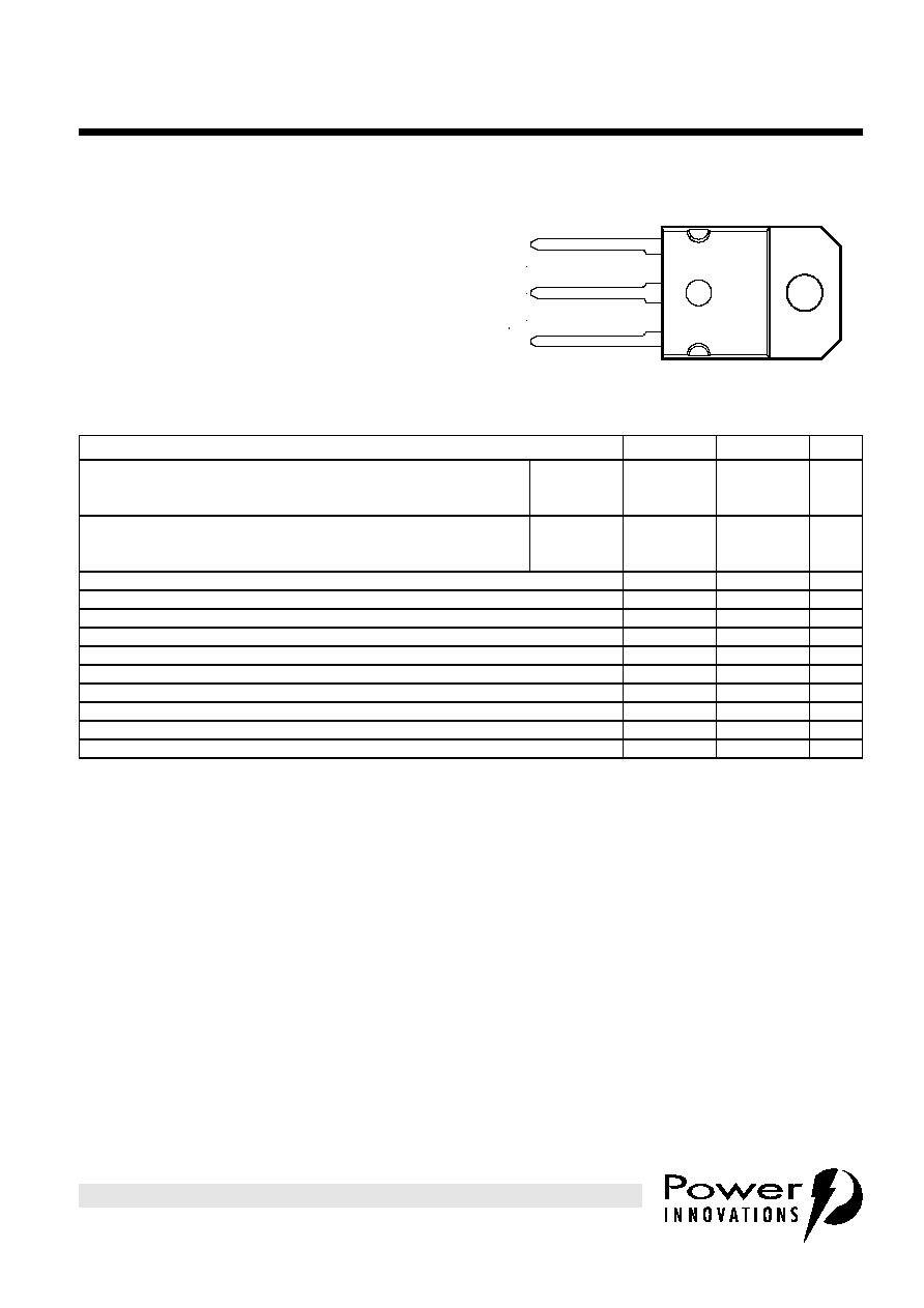
SOT-93 PACKAGE
(TOP VIEW)
Pin 2 is in electrical contact with the mounting base.
MDTRAA
B
C
E
1
2
3
absolute maximum ratings
at 25∞C case temperature (unless otherwise noted)
NOTES: 1. This value applies for t
p
10 ms, duty cycle
10%.
2. This value applies to the total collector-terminal current when the collector is at negative potential with respect to the emitter.
3. Derate linearly to 150∞C case temperature at the rate of 0.4 W/∞C.
4. Derate linearly to 150∞C free air temperature at the rate of 24 mW/∞C.
RATING
SYMBOL
VALUE
UNIT
Collector-base voltage (I
E
= 0)
TIP160
TIP161
TIP162
V
CBO
320
350
380
V
Collector-emitter voltage (I
B
= 0)
TIP160
TIP161
TIP162
V
CEO
320
350
380
V
Emitter-base voltage
V
EBO
5
V
Continuous collector current
I
C
10
A
Peak collector current (see Note 1)
I
CM
15
A
Peak commutating anti-parallel diode current (I
B
= 0) (see Note 2)
I
EM
10
A
Continuous base current
I
B
1
A
Continuous device dissipation at (or below) 100∞C case temperature (see Note 3)
P
tot
50
W
Continuous device dissipation at (or below) 25∞C free air temperature (see Note 4)
P
tot
3
W
Operating junction temperature range
T
j
-65 to +150
∞C
Storage temperature range
T
stg
-65 to +150
∞C
Lead temperature 3.2 mm from case for 10 seconds
T
L
260
∞C

TIP160, TIP161, TIP162
NPN SILICON POWER DARLINGTONS
2
JUNE 1973 - REVISED MARCH 1997
P R O D U C T I N F O R M A T I O N
NOTES: 5. These parameters must be measured using pulse techniques, t
p
= 300 µs, duty cycle
2%.
6. These parameters must be measured using voltage-sensing contacts, separate from the current carrying contacts.
Voltage and current values shown are nominal; exact values vary slightly with transistor parameters.
electrical characteristics at 25∞C case temperature
PARAMETER
TEST CONDITIONS
MIN
TYP
MAX
UNIT
I
CEO
Collector-emitter
cut-off current
V
CE
= 320 V
V
CE
= 350 V
V
CE
= 380 V
I
B
= 0
I
B
= 0
I
B
= 0
TIP160
TIP161
TIP162
1
mA
I
CEX(sus)
Collector-emitter
sustaining current
V
CLAMP
= V
(BR)CEO
7
A
I
EBO
Emitter cut-off
current
V
EB
= 5 V
I
C
= 0
100
mA
h
FE
Forward current
transfer ratio
V
CE
= 2.2 V
I
C
= 4 A
(see Notes 5 and 6)
200
V
CE(sat)
Collector-emitter
saturation voltage
I
B
= 0.1A
I
B
= 1 A
I
C
= 6.5 A
I
C
= 10 A
(see Notes 5 and 6)
2.8
2.9
V
V
BE(sat)
Base-emitter
saturation voltage
I
B
= 0.1A
I
C
= 6.5 A
(see Notes 5 and 6)
2.2
V
V
EC
Parallel diode
forward voltage
I
E
= 10 A
I
B
= 0
(see Notes 5 and 6)
3.5
V
thermal characteristics
PARAMETER
MIN
TYP
MAX
UNIT
R
JC
Junction to case thermal resistance
1
∞C/W
R
JA
Junction to free air thermal resistance
41.7
∞C/W
C
C
Thermal capacitance of case
1.4
J/∞C
resistive-load-switching characteristics at 25∞C case temperature
PARAMETER
TEST CONDITIONS
MIN
TYP
MAX
UNIT
t
d
Delay time
I
C
= 6.5 A
V
BE(off)
= -5 V
I
B(on)
= 100 mA
R
L
= 5
I
B(off)
= -100 mA
40
ns
t
r
Rise time
1.5
µs
t
s
Storage time
2.2
µs
t
f
Fall time
2.6
µs
3
JUNE 1973 - REVISED MARCH 1997
TIP160, TIP161, TIP162
NPN SILICON POWER DARLINGTONS
P R O D U C T I N F O R M A T I O N
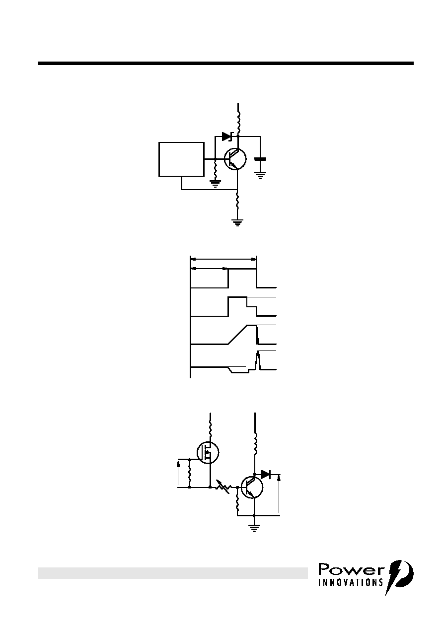
PARAMETER MEASUREMENT INFORMATION
Figure 1. Functional Test Circuit
Figure 2. Functional Test Waveforms
Figure 3. Switching Test Circuit
Driver and
Current
Limiting
Circuit
0.22
µ
µ
F
V z
24 V
L = 7 mH
100
0.2
TUT
Vclamp
Collector
Emitter
Voltage
16.6 ms
11.6 ms
0
0
0
0
Input
Signal
Base
Current
Collector
Current
24 V
IB
IC
40 V
12 V
0.056
IRF140
1 k
47
TUT
BY205-600
7 mH
Vclamp
Adjust for
I B
= 10 V
V in

TIP160, TIP161, TIP162
NPN SILICON POWER DARLINGTONS
4
JUNE 1973 - REVISED MARCH 1997
P R O D U C T I N F O R M A T I O N
TYPICAL CHARACTERISTICS
Figure 4.
Figure 5.
Figure 6.
Figure 7.
TYPICAL DC CURRENT GAIN
vs
COLLECTOR CURRENT
I
C
- Collector Current - A
0∑4
1∑0
10
40
h
FE
- Typical DC Current Gain
10
100
1000
10000
TCD160AA
V
CE
= 2.2 V
t
p
= 300 µs, duty cycle < 2%
T
C
= 125∞C
T
C
= 25∞C
T
C
= -30∞C
COLLECTOR-EMITTER SATURATION VOLTAGE
vs
COLLECTOR CURRENT
I
C
- Collector Current - A
1∑0
10
V
CE(sat)
- Collector-Emitter Saturation Voltage - V
0∑1
1∑0
10
TCD160AB
T
C
= 125∞C
T
C
= 25∞C
T
C
= -30∞C
I
C
/ I
B
= 65
t
p
= 300 µs, duty cycle < 2%
COLLECTOR-EMITTER SATURATION VOLTAGE
vs
COLLECTOR CURRENT
I
C
- Collector Current - A
1∑0
10
V
CE(sat)
- Collector-Emitter Saturation Voltage - V
0∑4
1∑0
4∑0
TCD160AD
T
C
= 125∞C
T
C
= 25∞C
T
C
= -30∞C
I
C
/ I
B
= 10
t
p
= 300 µs, duty cycle < 2%
BASE-EMITTER SATURATION VOLTAGE
vs
COLLECTOR CURRENT
I
C
- Collector Current - A
1∑0
10
V
BE(sat)
- Base-Emitter Saturation Voltage - V
0∑6
1∑0
3∑0
TCP160AC
T
C
= -30∞C
T
C
= 25∞C
T
C
= 125∞C
I
C
/ I
B
= 65
t
p
= 300µs, duty cycle < 2%

5
JUNE 1973 - REVISED MARCH 1997
TIP160, TIP161, TIP162
NPN SILICON POWER DARLINGTONS
P R O D U C T I N F O R M A T I O N
MAXIMUM SAFE OPERATING REGIONS
Figure 8.
MAXIMUM FORWARD-BIAS
SAFE OPERATING AREA
V
CE
- Collector-Emitter Voltage - V
1∑0
10
100
1000
I
C
- Collector Current - A
0∑01
0.1
1∑0
10
100
SAD160AA
TIP160
TIP161
TIP162
T
C
100
o
C
DC Operation
t
p
= 150 ms,
d = 1%
t
p
= 5 ms,
d = 5%
t
p
= 1 ms,
d = 5%
t
p
= 0.1 ms,
d = 5%