 | –≠–ª–µ–∫—Ç—Ä–æ–Ω–Ω—ã–π –∫–æ–º–ø–æ–Ω–µ–Ω—Ç: TIPL760A | –°–∫–∞—á–∞—Ç—å:  PDF PDF  ZIP ZIP |
TIPL760, TIPL760A
NPN SILICON POWER TRANSISTORS
P R O D U C T I N F O R M A T I O N
1
AUGUST 1978 - REVISED MARCH 1997
Copyright © 1997, Power Innovations Limited, UK
Information is current as of publication date. Products conform to specifications in accordance
with the terms of Power Innovations standard warranty. Production processing does not
necessarily include testing of all parameters.
q
Rugged Triple-Diffused Planar Construction
q
4 A Continuous Collector Current
q
Operating Characteristics Fully Guaranteed
at 100∞C
q
1000 Volt Blocking Capability
q
75 W at 25∞C Case Temperature
B
C
E
TO-220 PACKAGE
(TOP VIEW)
Pin 2 is in electrical contact with the mounting base.
MDTRACA
1
2
3
absolute maximum ratings
at 25∞C case temperature (unless otherwise noted)
NOTE
1: This value applies for t
p
10 ms, duty cycle
2%.
RATING
SYMBOL
VALUE
UNIT
Collector-base voltage (I
E
= 0)
TIPL760
TIPL760A
V
CBO
850
1000
V
Collector-emitter voltage (V
BE
= 0)
TIPL760
TIPL760A
V
CES
850
1000
V
Collector-emitter voltage (I
B
= 0)
TIPL760
TIPL760A
V
CEO
400
450
V
Emitter-base voltage
V
EBO
10
V
Continuous collector current
I
C
4
A
Peak collector current (see Note 1)
I
CM
8
A
Continuous device dissipation at (or below) 25∞C case temperature
P
tot
75
W
Operating junction temperature range
T
j
-65 to +150
∞C
Storage temperature range
T
stg
-65 to +150
∞C

TIPL760, TIPL760A
NPN SILICON POWER TRANSISTORS
2
AUGUST 1978 - REVISED MARCH 1997
P R O D U C T I N F O R M A T I O N
NOTES: 2. Inductive loop switching measurement.
3. These parameters must be measured using pulse techniques, t
p
= 300 µs, duty cycle
2%.
4. These parameters must be measured using voltage-sensing contacts, separate from the current carrying contacts.
Voltage and current values shown are nominal; exact values vary slightly with transistor parameters.
electrical characteristics at 25∞C case temperature (unless otherwise noted)
PARAMETER
TEST CONDITIONS
MIN
TYP
MAX
UNIT
V
CEO(sus)
Collector-emitter
sustaining voltage
I
C
= 10 mA
L = 25 mH
(see Note 2)
TIPL760
TIPL760A
400
450
V
I
CES
Collector-emitter
cut-off current
V
CE
= 850 V
V
CE
= 1000 V
V
CE
= 850 V
V
CE
= 1000 V
V
BE
= 0
V
BE
= 0
V
BE
= 0
V
BE
= 0
T
C
= 100∞C
T
C
= 100∞C
TIPL760
TIPL760A
TIPL760
TIPL760A
50
50
200
200
µA
I
CEO
Collector cut-off
current
V
CE
= 400 V
V
CE
= 450 V
I
B
= 0
I
B
= 0
TIPL760
TIPL760A
50
50
µA
I
EBO
Emitter cut-off
current
V
EB
= 10 V
I
C
= 0
1
mA
h
FE
Forward current
transfer ratio
V
CE
= 5 V
I
C
= 0.5 A
(see Notes 3 and 4)
20
60
V
CE(sat)
Collector-emitter
saturation voltage
I
B
= 0.5 A
I
B
= 0.8 A
I
B
= 0.8 A
I
C
= 2.5 A
I
C
= 4 A
I
C
= 4 A
(see Notes 3 and 4)
T
C
= 100∞C
1.0
2.5
5.0
V
V
BE(sat)
Base-emitter
saturation voltage
I
B
= 0.5 A
I
B
= 0.8 A
I
B
= 0.8 A
I
C
= 2.5 A
I
C
= 4 A
I
C
= 4 A
(see Notes 3 and 4)
T
C
= 100∞C
1.2
1.4
1.3
V
f
t
Current gain
bandwidth product
V
CE
= 10 V
I
C
= 0.5 A
f = 1 MHz
12
MHz
C
ob
Output capacitance
V
CB
= 20 V
I
E
= 0
f = 0.1 MHz
110
pF
thermal characteristics
PARAMETER
MIN
TYP
MAX
UNIT
R
JC
Junction to case thermal resistance
1.56
∞C/W
inductive-load-switching characteristics at 25∞C case temperature (unless otherwise noted)
PARAMETER
TEST CONDITIONS
MIN
TYP
MAX
UNIT
t
sv
Voltage storage time
I
C
= 4 A
V
BE(off)
= -5 V
I
B(on)
= 0.8 A
(see Figures 1 and 2)
2.5
µs
t
rv
Voltage rise time
300
ns
t
fi
Current fall time
250
ns
t
ti
Current tail time
150
ns
t
xo
Cross over time
400
ns
t
sv
Voltage storage time
I
C
= 4 A
V
BE(off)
= -5 V
I
B(on)
= 0.8 A
T
C
= 100∞C
(see Figures 1 and 2)
3
µs
t
rv
Voltage rise time
500
ns
t
fi
Current fall time
250
ns
t
ti
Current tail time
150
ns
t
xo
Cross over time
750
ns

3
AUGUST 1978 - REVISED MARCH 1997
TIPL760, TIPL760A
NPN SILICON POWER TRANSISTORS
P R O D U C T I N F O R M A T I O N
PARAMETER MEASUREMENT INFORMATION
Figure 1. Inductive-Load Switching Test Circuit
Figure 2. Inductive-Load Switching Waveforms
RB
(on)
V
BE(off)
Vclamp = 400 V
vcc
µ
µ
H
180
33
+5V
D45H11
BY205-400
BY205-400
2N2222
BY205-400
5X BY205-400
BY205-400
1 k
68
1 k
47
2N2904
D44H11
100
270
V Gen
+5V
1 k
0.02
µ
µ
F
TUT
1 pF
33
Adjust pw to obtain I
C
For I
C
< 6 A V
CC
= 50 V
For I
C
6 A V
CC
= 100 V
Base Current
A (90%)
I
B(on)
IB
Collector Voltage
Collector Current
D (90%)
E (10%)
F (2%)
C
B
90%
10%
V
CE
I
C(on)
A - B = t
sv
B - C = t
rv
D - E = t
fi
E - F = t
ti
B - E = t
xo
NOTES: A. Waveforms are monitored on an oscilloscope with the following characteristics: t
r
< 15 ns, R
in
> 10
, C
in
< 11.5 pF.
B. Resistors must be noninductive types.
TIPL760, TIPL760A
NPN SILICON POWER TRANSISTORS
4
AUGUST 1978 - REVISED MARCH 1997
P R O D U C T I N F O R M A T I O N
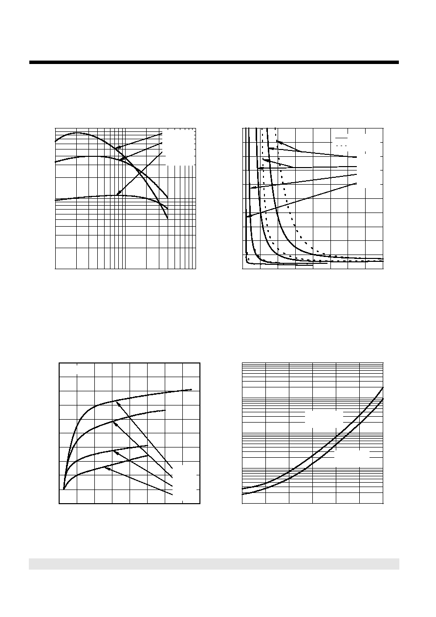
TYPICAL CHARACTERISTICS
Figure 3.
Figure 4.
Figure 5.
Figure 6.
TYPICAL DC CURRENT GAIN
vs
COLLECTOR CURRENT
I
C
- Collector Current - A
0∑1
1∑0
10
h
FE
- Typical DC Current Gain
1∑0
10
100
TCP741AA
V
CE
= 5 V
T
C
= 125∞C
T
C
= 25∞C
T
C
= -65∞C
COLLECTOR-EMITTER SATURATION VOLTAGE
vs
BASE CURRENT
I
B
- Base Current - A
0
0∑5
1∑0
1∑5
2∑0
V
CE(sat)
- Collector-Emitter Saturation Voltage - V
0
1∑0
2∑0
3∑0
4∑0
5∑0
TCP741AB
T
C
= 25∞C
T
C
= 100∞C
I
C
= 4 A
I
C
= 3 A
I
C
= 2 A
I
C
= 1 A
BASE-EMITTER SATURATION VOLTAGE
vs
BASE CURRENT
I
B
- Base Current - A
0
0∑2
0∑4
0∑6
0∑8
1∑0
1∑2
1∑4
1∑6
V
BE(sat)
- Base-Emitter Saturation Voltage - V
0∑75
0∑85
0∑95
1∑05
1∑15
1∑25
TCP741AC
T
C
= 25∞C
I
C
= 4 A
I
C
= 3 A
I
C
= 2 A
I
C
= 1 A
COLLECTOR CUT-OFF CURRENT
vs
CASE TEMPERATURE
T
C
- Case Temperature - ∞C
-60
-30
0
30
60
90
120
I
CES
- Collector Cut-off Current - µA
0∑001
0∑01
0∑1
1∑0
10
TCP741AP
TIPL760
V
CE
= 850 V
TIPL760A
V
CE
= 1000 V
5
AUGUST 1978 - REVISED MARCH 1997
TIPL760, TIPL760A
NPN SILICON POWER TRANSISTORS
P R O D U C T I N F O R M A T I O N
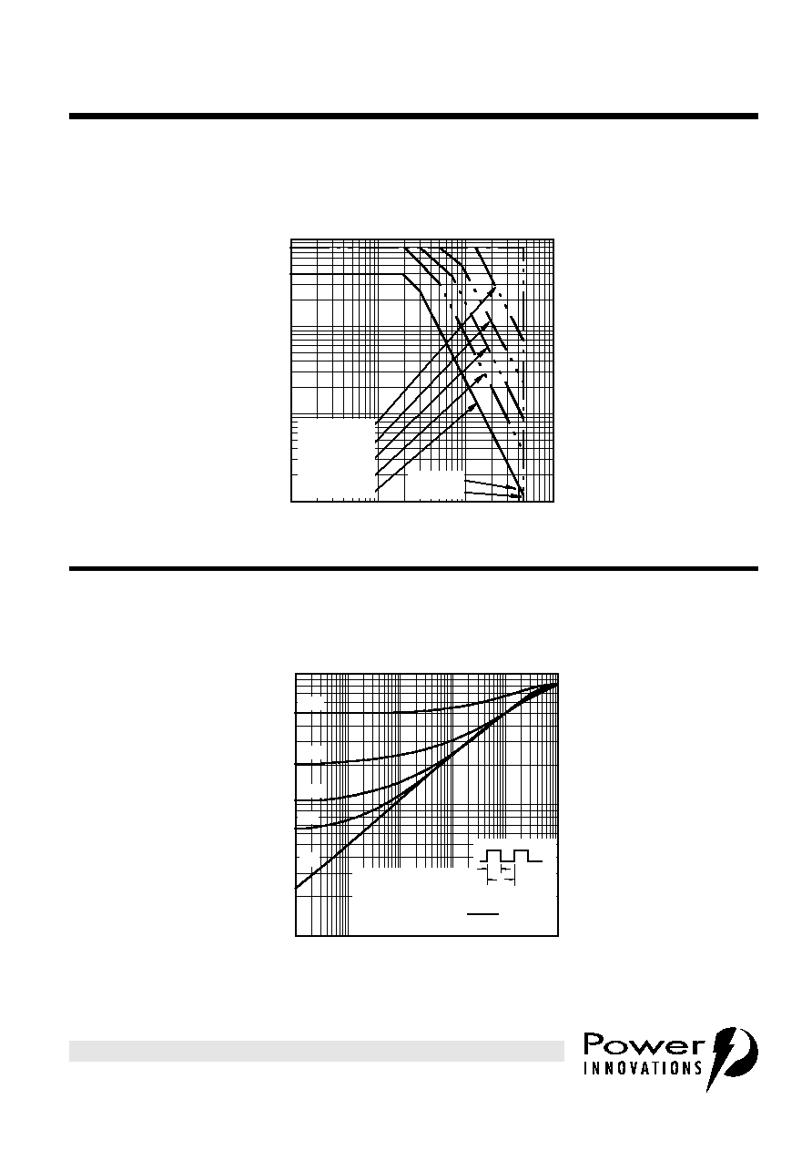
MAXIMUM SAFE OPERATING REGIONS
Figure 7.
THERMAL INFORMATION
Figure 8.
MAXIMUM FORWARD-BIAS
SAFE OPERATING AREA
V
CE
- Collector-Emitter Voltage - V
1∑0
10
100
1000
I
C
- Collector Current - A
0∑01
0.1
1∑0
10
SAP741AE
t
p
= 10
µ
µ
s
t
p
= 100
µ
µ
s
t
p
= 1 ms
t
p
= 10 ms
DC Operation
TIPL760
TIPL760A
THERMAL RESPONSE JUNCTION TO CASE
vs
POWER PULSE DURATION
t1 - Power Pulse Duration - s
10
-5
10
-4
10
-3
10
-2
10
-1
10
0
Z
JC
/R
JC
- Normalised Transient Thermal Impedance
0∑01
0∑1
1∑0
TCP741AM
t1
t2
duty cycle = t1/t2
Read time at end of t1,
T
J(max)
- T
C
= P
D(peak)
∑
∑ R
JC(max)
Z
JC
R
JC
( )
5%
10%
20%
50%
0%